
ALD1103
A DVANCED L INEAR
D EVICES, I NC.
DUAL N-CHANNEL AND DUAL P-CHANNEL MATCHED MOSFET PAIR
GENERAL DESCRIPTION
The ALD1103 is a monolithic dual N-channel and dual P-channel matched transistor pair intended for a broad range of analog applications. These enhancement-mode transistors are manufactured with Advanced Linear Devices' enhanced ACMOS silicon gate CMOS process. It consists of an ALD1101 N-channel MOSFET pair and an ALD1102 P-channel MOSFET pair in one package.
The ALD1103 offers high input impedance and negative current temperature coefficient. The transistor pair is matched for minimum offset voltage and differential thermal response, and it is designed for precision signal switching and amplifying applications in +2V to +12V systems where low input bias current, low input capacitance and fast switching speed are desired. Since these are MOSFET devices, they feature very large (almost infinite) current gain in a low frequency, or near DC, operating environment.When used in pairs, a dual CMOS analog switch can be constructed. In addition, the ALD1103 is intended as a building block for differential amplifier input stages, transmission gates, and multiplexer applications.The ALD1103 is suitable for use in precision applications which require very high current gain, beta, such as current mirrors and current sources.The high input impedance and the high DC current gain of the Field Effect Transistors result in extremely low current loss through the control gate.The DC current gain is limited by the gate input leakage current, which is specified at 50pA at room temperature. For example, DC beta of the device at a drain current of 5mA at 25°C is = 5mA/50pA = 100,000,000.FEATURES
?Thermal tracking between N-channel and P-channel pairs ?Low threshold voltage of 0.7V for both N-channel &P-channel MOSFETS ?Low input capacitance ?Low Vos -- 10mV
?High input impedance -- 1013? typical ?Low input and output leakage currents
?Negative current (I DS ) temperature coefficient ?Enhancement mode (normally off)?DC current gain 109
?Matched N-channel and matched P-channel in one package ?RoHS compliant
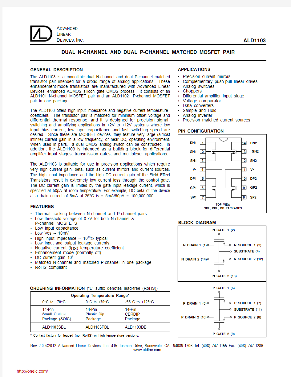
PIN CONFIGURATION
APPLICATIONS ?Precision current mirrors
?Complementary push-pull linear drives ?Analog switches ?Choppers
?Differential amplifier input stage ?Voltage comparator ?Data converters ?Sample and Hold ?Analog inverter
?
Precision matched current sources
DN2
GN2SN2GP2SP2
GN1SN1DP1GP11234567
8
91011121314DN1V +V -DP2SP1
BLOCK DIAGRAM
N SOURCE 1 (3)SUBSTRATE (4)
N SOURCE 2 (12)
N GATE 2 (13)
N DRAIN 1 (1) N GATE 1 (2)
N DRAIN 2 (14) P SOURCE 1 (7)SUBSTRATE (11)
P SOURCE 2 (8)
P GATE 2 (9)
P DRAIN 1 (5)
P GATE 1 (6)
P DRAIN 2 (10) TOP VIEW
SBL, PBL, DB PACKAGES
Operating Temperature Range*
0°C to +70°C 0°C to +70°C -55°C to +125°C 14-Pin
14-Pin 14-Pin Small Outline Plastic Dip CERDIP Package (SOIC)Package Package ALD1103SBL
ALD1103PBL
ALD1103DB
ORDERING INFORMATION (“L” suffix denotes lead-free (RoHS))
* Contact factory for leaded (non-RoHS) or high temperature versions.
ABSOLUTE MAXIMUM RATINGS
Drain-source voltage, V DS 10.6V Gate-source voltage, V GS 10.6V Power dissipation 500mW Operating temperature range SBL, PBL packages 0°C to +70°C
DB package-55°C to +125°C Storage temperature range-65°C to +150°C Lead temperature, 10 seconds +260°C CAUTION: ESD Sensitive Device. Use static control procedures in ESD controlled environment.
OPERATING ELECTRICAL CHARACTERISTICS
T A= 25°C unless otherwise specified
N - Channel Test P - Channel Test
Parameter Symbol Min Typ Max Unit Conditions Min Typ Max Unit Conditions
Gate Threshold V T0.40.7 1.0V I DS = 10μA V GS = V DS-0.4-0.7-1.2V I DS = -10μA V GS = V DS Voltage
Offset Voltage V OS10mV I DS = 100μA V GS = V DS10mV I DS = -100μA V GS = V DS V GS1 - V GS2
Gate Threshold
Temperature TC VT-1.2mV/°C-1.3mV/°C
Drift
On Drain I DS (ON)2540mA V GS = V DS = 5V-8-16mA V GS = V DS = -5V Current
Trans-.G fs510mmho V DS = 5V I DS= 10mA24mmho V DS = -5V I DS= -10mA conductance
Mismatch?G fs0.5%0.5%
Output G OS200μmho V DS = 5V I DS = 10mA500μmho V DS = -5V I DS = -10mA Conductance
Drain Source R DS(ON)5075?V DS = 0.1V V GS = 5V180270?V DS = -0.1V V GS = -5V ON Resistance
Drain Source
ON Resistance?R DS(ON)0.5%V DS = 0.1V V GS = 5V0.5%V DS = -0.1V V GS = -5V Mismatch
Drain Source
Breakdown BV DSS12V I DS = 10μA V GS =0V-12V I DS = -10μA V GS =0V Voltage
Off Drain I DS(OFF)0.14nA V DS =12V I GS = 0V0.14nA V DS = -12V V GS = 0V Current4μA T A = 125°C4μA T A = 125°C
Gate Leakage I GSS150pA V DS = 0V V GS =12V150pA V DS = 0V V GS =-12V Current10nA T A = 125°C10nA T A = 125°C
Input C ISS610pF610pF
Capacitance
OUTPUT CHARACTERISTICS
DRAIN - SOURCE VOLTAGE (V)
D R A I N - S O U R C
E C U R R E N T (m A )
-80-60
-40
-20
-8
-2
-6
-4
-10
-12
LOW VOLTAGE OUTPUT CHARACTERISTICS
DRAIN -SOURCE VOLTAGE (mV)D R A I N -S O U R C E C U R R E N T (m A )
-320
-1600160
320
-4
4
2
-2
-12
FORWARD TRANSCONDUCTANCE
vs. DRAIN - SOURCE VOLTAGE
DRAIN - SOURCE VOLTAGE (V)
-8
-2
-6
-4
-10
F O R W A R D T R A N S C O N D U C T A N C E (μm h o )
10000500020001000500200100
TRANSFER CHARACTERISTIC
WITH SUBSTRATE BIAS
GATE - SOURCE VOLTAGE (V)
-0.8
-1.6
-2.4
-3.2
-4.0
-20
-15
-10
-5
0D R A I N -S O U R C E C U R R E N T (μA )
GATE - SOURCE VOLTAGE (V)
R DS (ON) vs. GATE - SOURCE VOLTAGE
D R A I N - S O U R C
E O N
R E S I S T A N C E (?)
10000
1000
100
10
-2
-4
-6
-8
-10
-12
OFF DRAIN - CURRENT vs.
TEMPERATURE
TEMPERATURE (°C)
O F F - D R A I N S
O U R C E C U R R E N T (A )
-50
-25
+25
+50
+75
+125
+1000
-10X 10-6
-10X 10-12
-10X 10-9
OUTPUT CHARACTERISTICS
D R A I N -S O U R C
E C U R R E N T (m A )
160120
80
040
DRAIN-SOURCE VOLTAGE (V)
2
4
6
8
10
12
LOW VOLTAGE OUTPUT CHARACTERISTICS
DRAIN -SOURCE VOLTAGE (mV)D R A I N -S O U R C E C U R R E N T (m A )
-160
-80
080160
-88
4
-4
F O R W A R D T R A N S C O N D U C T A N C E
(μm h o )
FORWARD TRANSCONDUCTANCE vs. DRAIN-SOURCE VOLTAGE
DRAIN -SOURCE VOLTAGE (V)
1 x1055 x1041 x1045 x103
2 x1032 x1041 x103
2
4
6
8
10
12
GATE - SOURCE VOLTAGE (V)
TRANSFER CHARACTERISTIC
WITH SUBSTRATE BIAS
D R A I N
-S O U R C E C U R R E N T (μA )
20
15
10
5
00
0.8
1.6
2.4
3.2
4.0
GATE SOURCE VOLTAGE (V)
R DS (ON) vs. GATE - SOURCE VOLTAGE
D R A I N - S O U R C
E O N R E S I S T A N C E
(?)
10000
1000
100
10
2
4
6
8
10
12
OFF DRAIN - CURRENT vs.
TEMPERATURE
TEMPERATURE (°C)
O F F - D
R A I N S O U R C E C U R R E N T (A )
-50
-25
+25
+50
+75
+125
+1000
10X 10-6
10X 10-12
10X 10-9
DIFFERENTIAL AMPLIFIER
CURRENT SOURCE MULTIPLICATION
CURRENT SOURCE MIRROR
CURRENT SOURCE WITH GATE CONTROL
TYPICAL APPLICATIONS
I
Q 1, Q 2: N - Channel MOSFET Q 3, Q 4: P - Channel MOSFET
= 4
R SET
OUT IN -
V IN Q 1, Q 2: N - Channel MOSFET Q 3, Q 4
: P - Channel MOSFET
Q SET, Q 1..Q N : ALD 1101 or ALD 1103
N - Channel MOSFET
I SET = I SET x N
Q
ON
OFF
Q 3,Q 4 : P - Channel MOSFET
CASCODE CURRENT SOURCES
BASIC CURRENT SOURCES
P-CHANNEL CURRENT SOURCE
N-CHANNEL CURRENT SOURCE
TYPICAL APPLICATIONS (cont.)
I
+I SOURCE = I SET =
V + - Vt R SET =
V + - 1.0R SET
Q 1, Q 2 : N - Channel MOSFET ~= 4R SET
~+I Q 3, Q 4: P - Channel MOSFET
+I Q 1, Q 2, Q 3, Q 4: N - Channel MOSFET (ALD1101 or ALD1103)
Q1, Q2, Q3, Q4: P - Channel MOSFET
(ALD1102 or ALD1103)
I SOURCE = I SET =
V + - 2Vt
R SET
=
3 R SET
~
Millimeters Inches
Min Max Min Max Dim
A
A
1
b
C
D-14
E
e
H
L
S
1.75
0.25
0.45
0.25
8.75
4.05
6.30
0.937
8°
0.50
0.053
0.004
0.014
0.007
0.336
0.140
0.224
0.024
0°
0.010
0.069
0.010
0.018
0.010
0.345
0.160
0.248
0.037
8°
0.020
1.27 BSC0.050 BSC
1.35
0.10
0.35
0.18
8.55
3.50
5.70
0.60
0°
0.25
?
14 Pin Plastic SOIC Package
E
S (45°)
14 Pin Plastic DIP Package
1
Millimeters
Inches
Min Max Min Max Dim A A 1A 2b b 1c D-14E
E 1e e 1L
S-14?
3.810.381.270.890.380.2017.275.597.622.297.372.791.020°
5.081.272.031.650.510.3019.307.118.262.797.873.812.0315°
0.1050.0150.0500.0350.0150.0080.6800.2200.3000.0900.2900.1100.0400°
0.2000.0500.0800.0650.0200.0120.7600.2800.3250.1100.3100.1500.08015°
C
A
A1
b
b1
C
D-14
E
E1
e
e1
L
L1
L2
S
?
3.55
1.27
0.97
0.36
0.20
--
5.59
7.73
3.81
3.18
0.38
--
0°
5.08
2.16
1.65
0.58
0.38
19.94
7.87
8.26
5.08
--
1.78
2.49
15°
Millimeters Inches
Min Max Min Max Dim
0.140
0.050
0.038
0.014
0.008
--
0.220
0.290
0.150
0.125
0.015
--
0°
0.200
0.085
0.065
0.023
0.015
0.785
0.310
0.325
0.200
--
0.070
0.098
15°
2.54 BSC
7.62 BSC
0.100 BSC
0.300 BSC
14 Pin CERDIP Package
CERDIP-14 PACKAGE DRAWING
分销商库存信息:
ALD
ALD1103PBL ALD1103SBL