Diffusion lengths of silicon solar cells from luminescence images
- 格式:pdf
- 大小:1.45 MB
- 文档页数:10
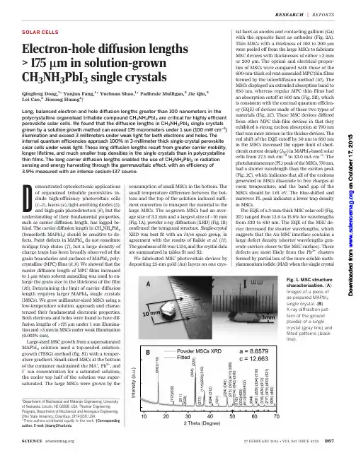
of organolead trihalide perovskites in-clude high-efficiency photovoltaic cells (1–3),lasers (4),light-emitting diodes (5),and high-gain photodetectors (6),but the understanding of their fundamental properties,such as carrier diffusion length,has lagged be-hind.The carrier diffusion length in CH 3NH 3PbI 3(henceforth MAPbI 3)should be sensitive to de-fects.Point defects in MAPbI 3do not constitute midgap trap states (7),but a large density of charge traps has been broadly observed at the grain boundaries and surfaces of MAPbI 3poly-crystalline (MPC)films (8,9).We showed that the carrier diffusion length of MPC films increased to 1m m when solvent annealing was used to en-large the grain size to the thickness of the film (10).Determining the limit of carrier diffusion length requires larger MAPbI 3single crystals (MSCs).We grew millimeter-sized MSCs using a low-temperature solution approach and charac-terized their fundamental electronic properties.Both electrons and holes were found to have dif-fusion lengths of >175m m under 1sun illumina-tion and >3mm in MSCs under weak illumination (0.003%sun).Large-sized MSC growth from a supersaturated MAPbI 3solution used a top-seeded solution-growth (TSSG)method (fig.S1)with a temper-ature gradient.Small-sized MSCs at the bottom of the container maintained the MA +,Pb 2+,and I –ion concentration for a saturated solution;the cooler top half of the solution was super-saturated.The large MSCs were grown by thesmall temperature difference between the bot-tom and the top of the solution induced suffi-cient convection to transport the material to the large MSCs.The as-grown MSCs had an aver-age size of 3.3mm and a largest size of ~10mm (Fig.1A);powder x-ray diffraction (XRD)(Fig.1B)confirmed the tetragonal structure.Single-crystal XRD was best fit with an I 4/m space group,in agreement with the results of Baikie et al .(11).The goodness of fit was 1.154,and the crystal data are summarized in tables S1and S2.We fabricated MSC photovoltaic devices by depositing 25-nm gold (Au)layers on one crys-tal facet as anodes and contacting gallium (Ga)with the opposite facet as cathodes (Fig.2A).Thin MSCs with a thickness of 100to 200m m were peeled off from the large MSCs to fabricate MSC devices with thicknesses of either >3mm or 200m m.The optical and electrical proper-ties of MSCs were compared with those of the 600-nm-thick solvent-annealed MPC thin films formed by the interdiffusion method (10).The MSCs displayed an extended absorption band to 850nm,whereas regular MPC thin films had an absorption cutoff at 800nm (Fig.2B),which is consistent with the external quantum efficien-cy (EQE)of devices made of these two types of materials (Fig.2C).These MSC devices differed from other MPC thin-film devices in that they exhibited a strong exciton absorption at 790nm that was more intense in the thicker devices.The red shift of the EQE cutoff by 50nm to 850nm in the MSCs increased the upper limit of short-circuit current density (J SC )in MAPbI 3-based solar cells from 27.5mA cm −2to 33.0mA cm −2.The photoluminescence (PL)peak of the MSCs,770nm,had a shorter wavelength than the exciton peak (Fig.2C),which indicates that all of the excitons generated in MSCs dissociate to free charges at room temperature;and the band gap of the MSCs should be 1.61eV.The blue-shifted and narrower PL peak indicates a lower trap density in MSCs.The EQE of a 3-mm-thick MSC solar cell (Fig.2D)ranged from 12.6to 15.8%for wavelengths from 520to 810nm.The EQE of the MSC de-vice decreased for shorter wavelengths,which suggests that the Au-MSC interface contains a large defect density (shorter wavelengths gen-erate carriers closer to the MSC surface).These defects are most likely from the Pb 2+clusters formed by partial loss of the more soluble meth-ylammonium iodide (MAI)when the single crystalSCIENCE 27FEBRUARY 2015•VOL 347ISSUE 62259671Department of Mechanical and Materials Engineering,University of Nebraska,Lincoln,NE 68588,USA.2Nuclear Engineering Program,Department of Mechanical and Aerospace Engineering,Ohio State University,Columbus,OH 43210,USA.*These authors contributed equally to this work.†Corresponding author.E-mail:jhuang2@Fig.1.MSC structure characterization.(A )Images of a piece of as-prepared MAPbI 3single crystal.(B )X-ray diffraction pat-tern of the ground powder of a single crystal (gray line)and fitted patterns (black line).RESEARCH |REPORTSo n O c t o b e r 17, 2015w w w .s c i e n c e m a g .o r g D o w n l o a d e d f r o mis removed from solution.Our recent density functional theory calculation verified that the Pb 2+clusters on the MAPbI 3surface tend to form charge traps (6).The internal quantum effici-ency (IQE)of the 3-mm MSC device (derived by dividing EQE by the transmittance of the Au electrode;see Fig.2D and fig.S2)was near unity (95T 7%).The electrons generated in the very thin pe-rovskite layer near the Au anode must traverse the whole crystal to be collected by the Ga cathode,indicating that the electron diffusion length in MSCs is greater than the crystal thick-ness (~3mm).We also replaced Ga by a semi-transparent Au (25nm)/C 60(25nm)layer as the cathode so that photogenerated charges would be located at the cathode side.Again,the value of J SC measured at 0.1%sun was comparable with incident light from both sides,which in-dicates that the hole diffusion length in MSCs is also longer than the MSC thickness.The dependence of responsivity (R )and J SC on light intensity (I L )for thick devices is sum-marized in Fig.2,E and F,respectively [see fig.S3for photocurrent density –voltage (J ph -V )curves].Under 1sun,the open-circuit voltage V oc was 0.62V,versus ~1.00V in optimized MPC thin-film devices,again indicating a strong charge recombination in the MSC devices under strong illumination.For thick MSC devices,R decreased from 35mA W −1to 0.19mA W −1when the in-tensity of white illuminated light increased from 0.003mW cm −2to 100mW cm −2because of in-creased charge recombination for higher I L .Fitting of J sc with I L as J sc ºI L b gave a value of b (recombination parameter)of 0.5T 0.01,which suggests that second-order charge recombina-tion dominated in the thick MSC devices for I L >0.003mW cm −2,as seen previously (12,13).Re-ducing the MSC thickness to 200m m recovered large R (Fig.2E)at 1sun and increased b to 0.88,which indicates that the carrier diffusion length of MSCs is near 200m m for 1sun illumination.We could characterize the carrier mobility m and carrier lifetime t r because the carrier diffu-sion length L D is determined by L D =(k B T m t r /e )1/2,where k B ,T ,and e are the Boltzmann constant,absolute temperature,and elementary charge,re-spectively.The device dark current (J D )was mea-sured to derive the trap density and carrier mobilities.The MSCs were sandwiched by two Au electrodes deposited by thermal evaporation to form hole-only devices.As shown in Fig.3A,the linear J D -V relation (green line)indicates an ohmic response at the low bias (<2.1V).A trap-filling process was identified by the marked in-crease of the current injection at a bias range of 2.1to 10.7V.The voltage at which all the traps are filled (trap-filled limit voltage V TFL )was deter-mined by the trap density (14):V TFL¼en t L 22ee 0ð1Þwhere L is the thickness of the MSCs,e (=32)is relative dielectric constant of MAPbI 3,and e 0is the vacuum permittivity.The trap density n t in MSCs was calculated to be 3.6×1010cm −3.Forfilms were also fabricated with PEDOT:PSS and Au as the hole injection electrodes (fig.S4).The calculated hole trap density in the MPC thin films was 2.0×1015cm −3,which is almost five orders of magnitude greater than in the MSCs.Thermal admittance spectroscopy (fig.S5)confirmed the reduction in trap density by two to three orders of magnitude in MSCs.Thus,the extraordinary carrier diffusion length in the MSCs is the result of largely suppressed trap density.When operat-ing in the trap-free space charge limit current (SCLC)regime above 10.7V,the dark current of the MSC was well fitted (Fig.3A,green line)by the Mott-Gurney law:J D ¼9ee 0m V 2b8L3ð2Þwhere V b is applied voltage.A large hole mobil-ity of 164T 25cm 2V −1s −1was derived from the curve fitting.The uncertainties we reportedmeasurements on 10nominally identical de-vices.Hall effect measurements revealed that the MSC was slightly p-doped,with a low free hole concentration of 9(T 2)×109cm −3(see supple-mentary materials).The hole mobility from Hall effect measurement was 105T 35cm 2V −1s −1,in agreement with the SCLC results.Similarly,the electron trap density and electron mobility of MSCs were measured with the electron-only de-vices,which had phenyl-C 61-butyric acid methyl (PCBM):C 60/Ga as both electrodes.A low elec-tron trap density of 4.5×1010cm −3was derived (Fig.3B),comparable to the hole trap density,and the electron mobility was 24.8T 4.1cm 2V −1s −1.Finally,we used time-of-flight (ToF)to verify the high electron mobilities of 24.0T 6.8cm 2V −1s −1(Fig.3,C and D).The electron and hole mobil-ities in MSCs are several times the intrinsic band transport mobility in MPC thin films (10)and polycrystals (15)measured by the Hall effect method96827FEBRUARY 2015•VOL 347ISSUE 6225 SCIENCERESEARCH |REPORTSand those measured by transient terahertz spec-troscopy (16),both of which measure band trans-port mobility.However,ToF and SCLC mobilities are sensitive to the presence of charge traps in the materials.The excellent agreement of Hall mobility with ToF and SCLC mobilities in the single-crystal MAPbI 3devices indicates that the band-tail states in the organolead trihalide pe-rovskite single crystals are negligible.We measured t r in MSCs with transient pho-tovoltaic (TPV)and impedance spectroscopy (IS)at different values of I L (Fig.4);at 1sun,the TPV and IS values of t r were 82T 5m s and 95T 8m s,respectively,more than 10times the t r values in the best thin-film devices with so-phisticated surface passivation (10).Combining the measured mobility and lifetime of MSCs,the hole diffusion length is 175T 25m m under 1sun.The measured bulk carrier lifetime can be un-derestimated because of the presence of surface charge recombination,so the bulk carrier diffu-sion length should exceed this value.Reducing the bias light intensity to 0.1sun increased t r to 234and 198m s by TPV and IS measurements,respectively,indicating a longer carrier diffusion length under weaker light intensity.The long carrier diffusion length of MAPbI 3can find direct application in x-ray and gamma-ray sensing and in radiation energy harvesting.Radiation is generally much weaker than 1sun but should penetrate the entire device.Details pertaining to the carrier diffusion length extrapo-lation under weak light,radiation measurement,simulation,and estimation of gammavoltaic ef-ficiency can be found in the supplementary mate-rials.We extrapolated a carrier recombination lifetime of 2.6T 0.2s and carrier diffusion length sum of 33T 5mm under a light intensity of 0.003mW cm −2from our 1sun data.The presence of surface recombination should reduce the carrier diffusion length,and the measured >3mm elec-tron and hole diffusion length under weak light is thus reasonable.We exposed the 3-mm MSC device to intense gamma radiation and measured the electric current generation.A cesium-137gam-ma irradiator of 102Ci yielded a persistent current of 36.3T 0.3nA,which corresponds to a photon-to-electron conversion efficiency of 3.9%and agrees with the theoretic estimation.The demonstrated high carrier mobility,car-rier lifetime,and diffusion length of the MSCs described above point to several new directions for the application of MAPbI 3materials in print-able electronics,lasers,and solar cells (4).The high PL quantum yield of MAPbI 3and the ex-cellent overlap of the PL spectra with the ab-sorption spectrum of the single crystal allow photon recycling in thick perovskite crystals by reabsorbing the emission (4,5).The demonstra-tion of a charge diffusion length that greatly exceeds the absorption depth of photons with energy larger than the band gap of perovskites implies that IQEs of essentially 100%can be achieved under the low internal electric fields at device working condition.REFERENCES AND NOTES1.S.D.Stranks et al .,Science 342,341–344(2013).2.M.M.Lee,J.Teuscher,T.Miyasaka,T.N.Murakami,H.J.Snaith,Science 338,643–647(2012).3. A.Mei et al .,Science 345,295–298(2014).4.G.Xing et al .,Nat.Mater.13,476–480(2014).5.Z.K.Tan et al .,Nat.Nanotechnol.9,687–692(2014).6.R.Dong et al .,Adv.Mater.10.1002/adma.201405116(2015).7.J.Kim,S.H.Lee,J.H.Lee,K.H.Hong,J.Phys.Chem.Lett.5,1312–1317(2014).8.N.K.Noel et al .,ACS Nano 8,9815–9821(2014).9.I.A.Shkrob,T.W.Marin,J.Phys.Chem.Lett.5,1066–1071(2014).10.Z.Xiao et al .,Adv.Mater.26,6503–6509(2014).11.T.Baikie et al .,J.Mater.Chem.A 1,5628–5641(2013).12.J.S.Manser,P.V.Kamat,Nat.Photonics 8,737–743(2014).13.S.D.Stranks et al .,Phys.Rev.A 2,034007(2014).14.R.H.Bube,J.Appl.Phys.33,1733–1737(1962).15.C.C.Stoumpos,C.D.Malliakas,M.G.Kanatzidis,Inorg.Chem.52,9019–9038(2013).16.C.Wehrenfennig,G.E.Eperon,M.B.Johnston,H.J.Snaith,L.M.Herz,Adv.Mater.26,1584–1589(2014).SCIENCE 27FEBRUARY 2015•VOL 347ISSUE 6225969Fig.3.Carrier mobility characterization of MSCs.(A and B )Current-voltage curve for a hole-only MSC device (A)and an electron-only MSC device (B).The insets show the device structure of hole-only and electron-only MSC devices,respectively.Three regions can be identified according to different values of the exponent n :n =1is the ohmic region,n =2is the SCLC region,and in between is the trap-filled limited region.(C )Schematic illustration of the device for the time-of-flight measurement.(D )The transient current curves of the MSC device show the normalized transient photocurrent under various reverse biases.The carrier transit time is determined by the intercept of the pretransit and posttransit asymptotes of the photocurrent,marked by solid blue circles.Inset shows the charge transit time versus the reciprocal of bias;the solid line is a linear fit to the data.Fig.4.Carrier recombination lifetime characterization of MSCs.(A and B )Impedance spectroscopies (A)and transient photovoltaic curves (B)of the MSC devices under 1sun and 0.1sun illumination,re-spectively,with incident light from the semitransparent Au anode.The TPV decay curves were fitted by a single-exponential decay function.The inset of (A)is the extracted charge recombination lifetime from IS measurement of the MSC device and the MPC thin film at various applied voltage biases under 1sun illumination.The inset of (B)is the extracted charge recombination lifetime from TPV measurement of the MSC device under various light bias intensities.RESEARCH |REPORTSACKNOWLEDGMENTSSupported by U.S.Department of Energy award DE-EE0006709(solar cell)and Defense Threat Reduction Agency award HDTRA1-14-1-0030(radiation detector).J.H.conceived the idea and supervised the project;Q.D.grew thesingle crystals and fabricated the devices;Q.D.,Y.F.,and Y.S.P.M.,J.Q.,and L.C.measured the devices under gamma ray irradiation and did the simulation;and J.H.wrote the paper.SUPPLEMENTARY MATERIALS/content/347/6225/967/suppl/DC1Figs.S1to S11Tables S1and S2References (17–21)27December 2014;accepted 20January 2015Published online 29January 2015;water is a promising means of storing solar energy in a way that compensates for the intermittency of sunlight as a primary source of power (1,2).It can be realized by apply-ing a hybrid system in which a solar cell powers an electrolyzer [photovoltaic (PV)electrolysis].Pho-toelectrolysis (PE)uses photocatalyst electrodes with additional electrical power provided by a photovoltaic element.Photocatalysis (PC)involves light-irradiated catalysts (typically catalyst pow-ders suspended in water)for water splitting (3).Recently reported “solar-to-hydrogen ”(STH)ef-ficiencies for PV electrolysis systems exceed 10%(4–6).State-of-the-art PE systems yield STH values of 2to 3%(7)but are believed to provide a cheaper solution for H 2production.PC is the simplest water-splitting approach,more ame-nable to cheap,large-scale applications of H 2generation.Unfortunately,despite intense efforts during the past 40years (8–15),current direct photocatalysts for water splitting still face several challenging issues:(i)Currently reported cata-lysts suffer from low quantum efficiency (QE)in the visible range,with STH efficiencies less thanof rare and expensive materials;(iii)various pho-tocatalysts show poor stability [e.g.,inorganic sulfide and (oxy)nitride-based photocatalysts are less stable and more susceptible to oxida-tion than water];(iv)O 2release from semi-conductor catalysts is difficult,so that the use of sacrificial reagents is required;(v)the overall four-electron water oxidation to O 2encounters a large overpotential;and (vi)the kinetically com-peting two-electron reaction to H 2O 2often poisons the photocatalysts (19).Overall water splitting to H 2and O 2requires a high free energy of 113.38kcal/mol (20,21).The challenge lies mainly in the release of diatomic O 2,which involves four electron and four pro-ton transfers for the eventual formation of an O-O bond.The concerted four-electron process for oxygen evolution (1.23eV)is thermodyna-mically more favorable than the two-electron process for H 2O 2formation (1.78eV).However,detailed analysis (see supplementary text)shows that a higher reaction rate may be achieved in a system where water is first oxidized via a two-electron reaction to H 2O 2and H 2,followed by H 2O 2decomposition to O 2and H 2O.For this stepwise two-electron/two-electron water splitting to H 2and O 2to be viable and practical,the photo-catalyst applied should be capable of promoting generation as well as subsequent decomposition of H 2O 2with high efficiencies and low overpo-tentials,so as to allow considerable reduction in the energy cost for production of H 2and O 2overall water splitting.Here,we report that nanocomposites of carbon nanodots embedded a C 3N 4matrix perform as an excellent photo-fulfilling the above requirements.C 3N 4is commercially available (e.g.,from Carbo-and can be easily fabricated (e.g.,from urea)19).It is an Earth-abundant and low-cost photo-capable of generating H 2and H 2O 2from even in the absence of catalytic metals,with a low QE (19,22–26).C 3N 4belongs to oldest reported polymer materials prepared chemists (by Berzelius in ~1830)and first “Melon ”(27).In 2006it was determined the visible light activity of TiO 2after treat-with urea was due to “Melon ”(28).In 2009,and colleagues described in detail the properties,electronic structure,and photo-activity of C 3N 4(29).Following this work,groups attempted to optimize the catalytic of C 3N 4,motivated by its relatively low gap energy E g of 2.7eV,and high valence and conduction band positions (29)[1.8–0.9eV versus reversible hydrogen electrode Many heterojunction composites with semiconductors as well as photocatalyst were investigated.The latter included systems with a variety of oxides (30)and sulfides (31)along with pure metals (19)and even graphene (32)and carbon nanotubes (33).Different prep-aration methods were studied in an effort to increase the surface area of C 3N 4and to improve its catalytic activity.The QE values obtained using C 3N 4as a catalyst for water splitting to H 2and O 2have been low (maximum 3.75%at 420nm and less than 0.5%for 500nm),and generally the use of a sacrificial reagent has been necessary (19,24,26,30–32,34).The efficiency at 700nm can be largely increased by applying dye mol-ecules,but again a sacrificial reagent is a must (35).During water splitting C 3N 4suffers from poi-soning by the produced H 2O 2,which is difficult to remove from the C 3N 4surface (19).Different methods including stirring,bubbling,and/or ad-dition of chemical agents have been attempted for regeneration of the poisoned C 3N 4catalyst (19).Carbon nanodots (CDots;monodisperse graph-ite particles less than 10nm in diameter)exhibit unique photo-induced electron transfer,photo-luminescence,and electron reservoir properties (36).In particular,CDots possess high catalytic activity (by chemical catalysis;no light is needed)for H 2O 2decomposition (37).Given the photo-catalytic properties of CDots and C 3N 4,we hypoth-esized that a combination of CDots and C 3N 4could constitute a high-performance composite photocatalyst for water splitting via the stepwise two-electron/two-electron process:(i)2H 2O →H 2O 2+H 2;(ii)2H 2O 2→2H 2O +O 2.97027FEBRUARY 2015•VOL 347ISSUE 6225 SCIENCE1Jiangsu Key Laboratory for Carbon-based FunctionalMaterials and Devices,Institute of Functional Nano and Soft Materials (FUNSOM),Soochow University,Suzhou 215123,China.2Department of Materials Science and Engineering,Technion,Israel Institute of Technology,Haifa 3200003,Israel.*Corresponding authors.E-mail:zhkang@ (Z.K.);apannale@ (S.-T.L.);shayli@tx.technion.ac.il (Y.L.)RESEARCH |REPORTSDOI: 10.1126/science.aaa5760, 967 (2015);347 Science et al.Qingfeng Dong single crystals 3PbI 3NH 3m in solution-grown CH µElectron-hole diffusion lengths > 175This copy is for your personal, non-commercial use only.clicking here.colleagues, clients, or customers by , you can order high-quality copies for your If you wish to distribute this article to othershere.following the guidelines can be obtained by Permission to republish or repurpose articles or portions of articles): October 17, 2015 (this information is current as of The following resources related to this article are available online at/content/347/6225/967.full.html version of this article at:including high-resolution figures, can be found in the online Updated information and services, /content/suppl/2015/01/28/science.aaa5760.DC1.htmlcan be found at:Supporting Online Material /content/347/6225/967.full.html#related found at:can be related to this article A list of selected additional articles on the Science Web sites /content/347/6225/967.full.html#ref-list-1, 3 of which can be accessed free:cites 20 articles This article /content/347/6225/967.full.html#related-urls 3 articles hosted by HighWire Press; see:cited by This article has been/cgi/collection/app_physics Physics, Appliedsubject collections:This article appears in the following registered trademark of AAAS.is a Science 2015 by the American Association for the Advancement of Science; all rights reserved. The title Copyright American Association for the Advancement of Science, 1200 New York Avenue NW, Washington, DC 20005. (print ISSN 0036-8075; online ISSN 1095-9203) is published weekly, except the last week in December, by the Science o n O c t o b e r 17, 2015w w w .s c i e n c e m a g .o r g D o w n l o a d e d f r o m。
2008年5月电工技术学报Vol.23 No. 5 第23卷第5期TRANSACTIONS OF CHINA ELECTROTECHNICAL SOCIETY May 2008 硅太阳能电池串联电阻的一种估算新方法廖志凌1, 2阮新波1(1. 南京航空航天大学航空电源重点实验室南京 2100162. 江苏大学电气信息工程学院镇江 212013)摘要硅太阳能电池等效串联电阻会影响其正向伏安特性和短路电流,而对开路电压没有影响,另外串联电阻的增大会使太阳能电池的填充因子和光电转换效率降低。
研究计算太阳能电池串联电阻具有重要的实际意义。
提出一种估算太阳能电池串联电阻的新方法,利用太阳能电池生产厂商提供的在标准测试条件下的四个技术参数(短路电流I sc,开路电压V oc,最大功率点电流I m和电压V m)进行计算,同时通过引入相应补偿系数来考虑太阳光强和电池温度变化时对串联电阻的影响。
理论估算结果与实验测量结果比较,两者误差在工程应用允许的精度6%以下。
关键词:硅太阳能电池光伏发电串联电阻估算方法中图分类号:TK513A New Method on Computing Series Resistance of Silicon Solar CellsLiao Zhiling1, 2 Ruan Xinbo1(1. Nanjing University of Aeronautics and Astronautics Nanjing 210016 China2. Jiangsu University Zhenjiang 212013 China)Abstract The equivalent series resistance of silicon solar cell can influence its straight volt-ampere property and short-circuit current, but have no influence on open-circuit voltage. Moreover, the increase of series resistance can reduce the solar cell’s fill factor and conversion efficiency.Research on computing the series resistance of silicon solar cell has the important meaning. A new method on computing series resistance of silicon solar cells is proposed, which uses only four electrical parameters (the short-circuit current I sc, the open-circuit voltage V oc, the current of maximum power point I m, the voltage of maximum power point V m) under standard test conditions provided by manufacture. And the influence of variational solar radiation and solar cell temperature on series resistance of solar cell is taken into account with three additional compensation parameters. According to the comparison between theoretic computing datum and experimental datum of silicon solar cells, the result is satisfactory and the difference is found to be less than 6 percent.Keywords:Silicon solar cell,photovoltaic,series resistance,computing method1引言当今世界能源结构是以煤炭、石油和天然气等化石能源为主体,而化石能源是不可再生能源,大量耗用终将枯竭。
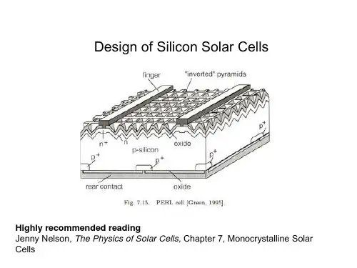
PERFORMANCE INSTABILITY IN N-TYPE PERT SILICON SOLAR CELLS Jianhua Zhao1, Jan Schmidt2, Aihua Wang1, Guangchun Zhang1, Bryce S. Richards1 and Martin A. Green11. Centre of Excellence for Advanced Silicon Photovoltaics and Photonics,University of New South Wales, Sydney, NSW 2052, Australia2. Institut für Solarenergieforschung Hameln/Emmerthal (ISFH),Am Ohrberg 1, D-31860 Emmerthal, GermanyABSTRACTPERT (passivated emitter, rear totally-diffused) cellson CZ and FZ n-type silicon substrates have demonstratedhigh efficiencies of 21.1% and 21.9%, respectively.Performance loss has been observed in these cells afterover two-year storage. A further loss was observed whenthese cells were illuminated under one-sun intensity usingELH halogen projection lamps. The lightly doped boronemitters and strong surface depletion might be the causefor such loss, which appear to have an electrostatic originand to be largely reversible.1.INTRODUCTIONFabricating solar cells on n-type CZ silicon substratesforms part of an international effort to solve thedegradation problem for cells on boron doped p-type CZsilicon substrates [1]. PERT cells on CZ and FZ n-typesilicon substrates (see Fig. 1) have demonstrated highefficiencies of 21.1% and 21.9%, respectively [2]. Fig. 1shows the structure of n-PERT cells. BBr3 liquid sourcediffusion is used to form the boron doped emitters. Thefront surfaces of these cells are further passivated by athermally grown 200Å thin silicon dioxide (SiO2), and asubsequent “alneal” (aluminium anneal) process. Thealneal process provides excellent surface passivation, andhence these n-PERT cells give high open-circuit voltages,V oc, close to 700 mV [2].p+pn-siliconthin oxide (~200Å) oxiderear contact finger"inverted" pyramidsn+n+n+double layerantireflectioncoatingnnFig. 1. PERT cell structure on n-type substrate.Directly after fabrication, these cells showed stable performance after a short period of illumination and a few weeks storage. The effective carrier lifetime measurement of such substrate passivated by TCA grown SiO2 have also shown stable performance after a few weeks storage and a few hours illumination by ELH lamps at one-sun intensity.2.DEGRADATION DURING STORAGE OF N-PERT CELLSHowever, in a recent study into these n-type PERT cells which were made two to three years ago, it was found that most of the cells have suffered large losses in their V oc up to 100 mV (see Fig. 2(a)). The cells in the left part in Fig. 2(a) were fabricated earlier than the cells in the right, with about one year time span. The latest cells in Fig.2(a) were made about 2 years ago. These cells were stored in a nitrogen box kept in a dimmed room light condition. It is seen that the earlier cells degraded much more than the later cells. The cells degraded by severely an average of 38 mV in V oc.(a)(b)Fig. 2. Comparison of performance loss after a few years storage of (a) PERT cells on n-type substrates, and (b) PERL cells on p-type substrates. The solid triangles are the performance before storage, and the hollow squares are those after storage.Due to the observation of the performance loss in the n-PERT cells, similar test were made to some even earlier fabricated PERL (passivated emitter, rear locally-diffused) cells on p-type substrates (see Fig. 2(b)). All these p-PERL cells, which were fabricated 3 to 9 years ago showed much smaller and more uniform changes, with little relation to the fabrication time and cell performance.The average V oc reduction of these p-PERL cells after N2 storage is 4.2 mV. However, because the short-circuit current density, J sc, of some unscribed cells was not properly calibrated due to the peripheral current collection, a large error was generated by the direct V oc comparison after storage. This error can be reduced when V oc reduction is corrected to an average 2.5 mV, assuming the cell J sc has no degradation. This assumption is reasonable for p-PERL cells, since V oc is much more sensitive than J sc to the changes in total recombination rate.3.FURTHER ILLUMINATION DEGRADATIONThe stability of un-encapsulated n-PERT and other types of cells was further examined by illuminating them under one-sun intensity from ELH lamps. Such ELH lamps possess a very small UV component, which results in similar conditions when encapsulated under glass. A further degradation has been observed (see Fig. 3).ocillumination by ELH lamps.In Fig. 3, the solid triangles from cell Wn10-3a represent the V oc of a PERT cell on an n-type FZ substrate. This cell had a high V oc of 693 mV after fabrication 3 years ago. Its V oc has degraded to 686 mV after 3 years storage in nitrogen. After 11 hours one-sun illumination, its V oc has further quickly degraded to 675.5 mV. Even this value was still degrading without reaching saturation when the experiment was stoped. This represents close to 20 mV degradation after storage and a short time illumination. It is clearly one of the least stable cells among all the tested cells.It is possible that the small UV component in the light source could generate electrical charges in the space between the ELH lamp and the cell, which can deposit on the cell surface. Hence, at the end of the degradation curve, the cell surface was charged with negative corona charging. Charged surfaces can vary the surface recombination velocity, but not affect the bulk recombination. After illumination degradation, the charged V oc could not recover to the value at fabrication, which shows some physical change has occurred.It was thought that the change may be associated with the 200Å thin passivation oxide, or with the inverted pyramid structure giving (111) surfaces. Hence, one planar n-PERL cell, X1-159R, with 1100Å thick passivation oxide made 10 years ago and stored in an office cabinet was also tested (not shown in Fig. 3). However, the V oc of this planar cell had degraded from about 690 mV at fabrication to the present 593mV. This gives about 100 mV in V oc degradation during 10 year storage. It makes it clear that a planar surface with thick passivation oxide does not help for the n-type cell stability.The illuminated V oc curves of the earlier rear boron emitter cells on n-type substrates, X1-294L and X1-294R, are also shown in Fig. 3. The initial V oc data of these cells could not be found, but they should be close to 690 mV, according to similar cells made at that time. Both cells had relatively large storage degradation of about 15 mV. It is interesting that these cells showed even greater illumination degradation rate, and did not reach saturation after losing a further 20 mV in 23 hours of illumination.A positive corona charging at the end of illumination recovered V oc to its fabrication value of over 690 mV for cell X1-294L. This suggests no permanent changes to this cell, with the voltage changes attributed to a changing electrostatic environment.The p-PERT cells [3] with an entire rear light boron diffusion on SEH 1.2 Ω-cm FZ(B) substrate has a similar rear surface condition as the rear boron n-PERL cells, X1-294L and X1-294R. One of these p-PERT cells, Ws8-4a, with very high initial V oc of 708.2 mV, was tested. It gives 7.7 mV storage degradation, and further 6.8 mV degradation in 38-hour illumination. It is clear that this p-PERT cell is much more stable than the n-PERT and n-PERL cells. Electrostatic charging restored the cell voltage to its original value, again suggesting no permanent change.A couple of p-PERL cells [3], Wh15-1f and Wh15-1d, were also tested. Wh15-1f showed a slightly less storage and illuminated V oc degradation than the p-PERT cell. The other p-PERL cell, Wh15-1d, had relatively large 8.8 mV storage V oc degradation. This cell was illuminated initially in short circuit conditions for the first 20 hours, and then changed to open circuit conditions. This cell gave a very stable illumination performance and circuit condition did not seem affect its performance. At the endof degradation curves, positive charges are deposited onto the surfaces all the p-type PERL and PERT cells. This recovered cell V oc to their original values. Hence, this verifies that the V oc reduction was due to the surface charge change, instead of any permanent degradation.To be noted here is that high efficiency p-PERL cells had been encapsulated and exposed to outdoor direct sunlight in stability tests in 1991 and 1996. Minimum V oc degradation was observed during those tests. From the present illuminated V oc degradation tests, it seems that the cells storage in nitrogen for long time may enhance the illuminated degradation. Hence, it is planned to have some n-PERT cells encapsulated as the previous p-PERL cells for outdoor sunlight illumination test. However, once the cell is encapsulated, it will be difficult to measure the cell temperature, which might generate large errors inV oc measurement.For comparison, the previous illumination measurement of p-PERT cells on CZ(Ga) substrates, Ws4-4c, Ws4-4e, Ws12-3c and Ws12-3e [4], is also shown in Fig. 3. These cells exhibited virtually no V oc change.4.BORON PROFILES BY SRA AND SIMS TESTSThe boron emitter profiles of the n-PERT cells were recently tested by SRA (spreading resistance analysis) (see Fig. 4). SIMS (Secondary Ion Mass Spectrometry) testalso showed similar boron profiles for cell Wn10-3. In Fig. 4, the high noise levels in Wn16-3 and Wn10-3 by SRA is due to the rough bright etched wafers surfaces, which distorted the depth positions when a flat bevel is used to enlarge the depth profile. In contrast, cell Wn1-6 has a very smooth boron profile due to its mechanically polished mirror surface finish.5.2. IQE Measurement of Different Cells1.E +141.E +151.E +161.E +171.E +181.E +190.511.5D epth (m ic ron)C a r r i e r C o n c e n t r a t i o n (c m -3)2The IQE (internal quantum efficiency) of different cells were also measured at UNSW and compared to the initial measurement results from Sandia many years ago when the cells were freshly made (see Fig. 6). It can be seen that the p-PERL cell, W4-19-6e, and rear boron emitter n-PERL cell, X1-280R, exhibited very little change in their short-wavelength IQE. On the contrary, the front boron emitter n-PERT cell, Wn10-6a, showed a significant reduction in the short-wavelength IQE, corresponding to a significant increase of the surface recombination in this cell. Using PC-1D simulation, this represents a surface recombination velocity of 25000 cm/s. Correspondingly, the V oc of this cell has degraded from 699 mV at fabrication, to 657.5 mV. This cell was measured at Sandia, and gives a higher degradation than the other cells stored in nitrogen at UNSW. It is not sure if the transportation to Sandia, or storage in air has caused this extra degradation.Fig. 4. Boron emitter profiles for a few n-PERT cells tested by SRA (spreading resistance analysis).In spite of the distortion in the profiles, the SRA results give some important information. Firstly, most of the profiles have rather light boron doping levels, as a result from searching for the highest cell efficiencies. Secondly, most of the cells have deep junctions. Thirdly and maybe the most importantly, there is a profound surface depletion in the boron profiles. Such surface depletion might significantly enhance the effect of surface recombination to the cell performance, and hance reduce the cell stability, under electrostatic changes at the surface.fabrication, and at UNSW after storage for a few years.5.3. Corona Charging Test5. OTHER EXPERIMENTS ON SURFACEPASSIVATION QUALITY Corona charging can deposit either positive or negative electrical charges onto the solar cell surface and hence changes the surface recombination rate. Fig.7. shows the corona charging result for an n-PERT cell, Wn10-3e.5.1. LBIC TestSpatially resolved LBIC (light beam induced current) measurements were performed at a wavelength of 633 nm to investigate the emitter uniformity. Low and uneven LBIC results (see Fig. 5) have been seen in the test pattern for these n-PERL cells. A previous study using Lock-in Thermography at Max Planck Institute of Microstructure Physics, Halle, also showed a highly non-uniform boron emitter and higher temperature rise than p-PERL cells [2].Wn8-3cResolution: 55.6umLaser wavelength: 633 nm With Bias LightFig. 7. Corona charging of an n-PERT cell.From the initial degraded state of 661 mV for V oc , the negative charges lifted V oc to 692.4 mV, which is 4.8 mV higher than when the cell was freshly fabricated. The positive charge initially reduce V oc , and then increase it again to a saturation value of 689.5 mV. Charging theFig. 5. LBIC image of the n-PERT cell emitter.thick oxide planar n-PERL cells and rear boron emitter n-PERL cells gave similar results as shown in Fig. 7. The corona charging experiment confirms that the V oc loss is due to electrostatic effects at the cell surface, while the bulk carrier lifetime does not degrade at all.It has been suggested that the lightly doped n-type surface might be easily inverted which generates a shunting channel [5]. However, charging the peripheral areas of the n-PERT cells did not affect the cell performance. It was confirmed that all the V oc change during charging comes from the cell active area, possibly due to the low substrate resistivity in these cells.5.4. SiN x Passivation ExperimentDepositing SiN x film with remote plasma has been used to improve the surface passivation for silicon cells [6]. Hence, such SiN x films have been deposited on to the n-PERT cells, some with passivating SiO 2 layer removed. It was found that the cells performance recovered to their original V oc in 690 mV range for SiN x /SiO 2 passivation. Unfortunately, the performances of these SiN x /SiO 2 passivated cells degraded even more quickly than the standard n-PERT cells with the SiO 2 surface passivation, both during shipping and during exposure to light.Fig. 9. PC-1D simulation results show that a heavier and shallow front boron emitter can markedly improve cell stability.7. CONCLUSIONSThe analysis on the emitter doping profiles by SRA (spreading resistance analysis) and SIMS (Secondary Ion Mass Spectrometry) has revealed very light emitter boron profiles and significant boron depletion at the emitter surface of n-type PERT cells. The boron surface depletion may have enhanced the instability of these cells. Changing the surface conditions using the corona charging strongly affects the cell performance. Depositing silicon nitride passivation layer with a remote plasma source can also recover some of the degradation, particularly for SiN x /SiO 2 passivation. Unfortunately, the SiN x /SiO 2 passivated cells still degrade fast after the SiN x deposition. It is expected that a heavier emitter boron profile with less surface boron depletion may significantly improve the performance of such cells, by improving tolerance to changing surface electrostatic conditions.6. PC-1D SIMULATIONThe performance of the front boron emitter n-PERT cells has been simulated with PC-1D (see Fig. 8). The surface boron depletion detected by SRA and SIMS measurement are incorporated into the calculation by including a secondary lighter and shallower n+ diffusion to compensate some surface boron. This surface depletion effect has significantly reduced V oc for certain front surface recombination velocities. Also, the simulated result shows V oc is expected to degrade much earlier than J sc if surface recombination velocity increases. This is the case for the n-PERT cells, in which the V oc was the most degraded factor, while their J sc remained basically unchanged during V oc degradation.ACKNOWLEDGMENTThe authors would like to thank P. Verlinden at Origin Energy for discussions about the n-type cells.REFERENCES[1] T. Saitoh, et al. "Light Degradation and Control ofLow-Resistivity CZ-Si Solar Cells --An International Joint Research--", Technical Digest of the 11th International Photovoltaic Science and Engineering Conference, Sapporo, Japan, pp.553-556, Sept., 1999. [2] J. Zhao, A. Wang, P.P. Altermatt, M. A. Green, J. P.Rakotoniaina and O. Breitenstein, “High Efficiency PERT Cells on N-Type Silicon Substrates”, Proceedings of the 29th IEEE Photovoltaic Specialist Conference, New Orleans, pp.218-221, May, 2002. [3] J. Zhao, A. Wang and M.A. Green, “24.5%Efficiency Silicon PERT Cells on MCZ Substrates and 24.7% Efficiency PERL Cells on FZ Substrates”, Progress in Photovoltaics, Vol. 7, pp. 471-474, 1999. Fig. 8. PC-1D simulation of the n-PERT cell performance. [4] J. Zhao, A. Wang, M.A. Green, “High EfficiencyPERT Cells on a Variety of Single Crystalline Silicon Substrates”, Proceedings of the 16th European Photovoltaic Solar Energy Conference and Exhibition, Glasgow, UK, pp.1100-1103, May, 2000.A further simulation with PC-1D has shown that an increased boron doping level is beneficial to n-PERT cell stability. Another fact is that the surface depletion in the boron profile is reduced for heavier boron diffusion, according to the SRA measurement (see Fig. 4.). This further improves the cell stability. If the boron junction depth can also be reduced, both V oc and J sc degradations can be reduced (see Fig. 9).[5] P. Verlinden, Private communication, 2003.[6] A. Hubner, A.G. Aberle and R. Hezel, “20% EfficientBifacial Silicon Solar Cells, Conf. Record 14th European Photovoltaic Solar Energy Conference, pp. 92, 1997.。
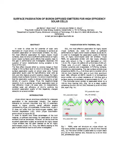
SURFACE PASSIVATION OF BORON DIFFUSED EMITTERS FOR HIGH EFFICIENCYSOLAR CELLSJan Benick1, Bram Hoex2, O. Schultz and Stefan W. Glunz11Fraunhofer Institute for Solar Energy Systems, Heidenhofstr. 2, 79110 Freiburg, Germany 2Department of Applied Physics, Eindhoven University of Technology, P.O. Box 513, 5600 MB Eindhoven, TheNetherlandse-mail: jan.benick@ise.fraunhofer.deABSTRACTIn order to utilize the full potential of solar cells fabricated on n-type silicon, it is necessary to achieve an excellent passivation on boron-doped emitters. As SiO2, the most effective passivation for highly doped n-type surfaces, does not show a sufficient performance on highly boron doped surfaces some effects that possibly lead to this gap in performance are investigated. Especially the question of boron redistribution during oxidation is the focus of this work.The field effect induced either by corona charge or fixed charge in the surface layer is known to strongly affect the surface passivation quality on silicon solar cells. Typical passivation layers used for high-efficiency solar cells as SiO2 and SiN x feature a built-in positive charge. For highly doped p-type surfaces however, it is shown experimentally that the passivation quality is strongly enhanced by a high density of negative charge. Thus, the negative-charge dielectric Al2O3 is applied as surface passivation layer on high efficiency n-type c-Si solar cells. An independently certified solar cell efficiency of 23.2 % confirms the excellent passivation quality of this negatively charged dielectric on a boron emitter.INTRODUCTIONn-type silicon has an enormous potential for widescale application in the photovoltaic industry. The relative tolerance to common impurities (e.g. Fe) [1] potentially results in higher minority carrier diffusion lengths compared to p-type c-Si substrates. Furthermore, n-type c-Si does not suffer from the boron-oxygen related, light- induced degradation (LID), which p-type Czochralski-grown silicon is known for [2].In order to benefit from these advantages of the bulk material, a sufficient technology for passivation of boron emitters must be developed. However, on device level the excellent passivation quality as achieved for highly doped n-type emitters has not been realized so far for highly boron-doped p-type c-Si. Thus, the effects leading to this gap in performance have to be further investigated.PASSIVATION WITH THERMAL SIO2SiO2, the most effective passivation for highly dopedn-type surfaces [3], does not show a sufficient performance on highly boron doped surfaces [4] [5] [6] [7].In order to investigate the passivation quality of thermalSiO2 on highly boron-doped solar cell emitters, n-typePERL [3] (passivated emitter with rear locally diffused)solar cells (shown in Fig. 1) were fabricated on 〈100〉1 Ω cm, FZ, n-type c-Si wafers with a thickness of 250 µm.These cells (A = 4 cm2) feature a front surface withinverted pyramids and evaporated Al/Ti/Pd/Ag contacts,thickened by electroplating. The rear surface exhibits local phosphorus BSFs (R sheet≈ 20 Ω/sq) and is covered with a100 nm thick thermal SiO2 and a 2 µm thick aluminumlayer. BBr3 diffusion at 890°C results in a homogenousboron emitter with a sheet resistance of 130 Ω/sq and asurface doping concentration of approximately 8×1019 cm-3. This front-side boron emitter is passivated either by a105 nm thick thermal SiO2 (Fig. 1a) or a stack systemconsisting of a thin (30 nm) SiO2 followed by a 40 nm thickSiN x layer (Fig. 1b).(a) (b)Fig. 1 PERL solar cell structure on n-type silicon. (a)The boron emitter is passivated by a 105 nm thick thermalSiO2. (b) The boron emitter is passivated by a layer stackof a 30 nm thick thermal SiO2 followed by a 40 nm thickSiN x antireflection layer.The one-sun parameters of these cells are summarized in Table 1. The solar cells passivated by the SiO 2/SiN layer stack show a higher conversion efficiency (20.4 %) compared to the solar cells passivated by the 105 nm thick thermal SiO 2 (19.5 %). This gain in performance can be attributed to a higher short-circuit current due to better antireflection characteristics of the layer stack system as shown in Fig. 2. The open-circuit voltage (V oc ), a measure for passivation quality, is the same for both passivation layers. The relatively low values of only 638 mV reached for these cells indicate a poor passivation quality which is assumed to be due to an insufficient passivation of the boron emitter by the thermal SiO 2.Table 1 Results of n -type PERL solar cells passivated by thermal SiO 2 (AM1.5G, 100 mW/cm 2, 25°C). Passivation layerV oc [mV]j sc [mA/cm 2]FF [%] η [%] av. 636.7 ± 3.6 39.2± 0.3 78.4 ± 0.319.6 ± 1.0SiO 2 + SiNbest 638.139.780.6 20.4 av. 636.3 ± 1.4 37.8± 0.2 79.6± 0.219.1 ± 0.5105 nm SiO 2best 638.538.080.3 19.5The strong drop of the internal quantum efficiency (IQE) in the short wavelength range (below ~600 nm) for both passivation systems confirms this assumption of an insufficient passivation of the boron emitter.I Q Ewavelength [nm]Fig. 2 IQE and reflection of n -type PERL solar cells passivated by thermal SiO 2.As the solubility of the boron is higher in SiO 2 than in Si the oxidation process might cause a surface depletion of the boron emitter as described by other researchers [7] [8]. Such a surface depletion would be detrimental for surface passivation. To investigate this effect, FZ n -type Si wafers with identical boron emitters (R sheet = 130 Ω/sq) were oxidized at different temperatures resulting in SiO 2thicknesses between 10 and 105 nm. The resulting boron profiles were measured by electrochemical capacitance-voltage profiling (ECV) (see Fig. 3). A surface depletion of the boron emitter could only be observed for the oxidation process that resulted in a very thin (10 nm) SiO 2. The diffusion profiles of the remaining boron emitters which received an oxidation process that led to a thicker SiO 2, do not show a significant surface depletion. As the SiO 2 passivation layers which are applied at our solar cells exceed this critical thickness the effect of surface depletion of the boron emitter is probably not the reason for the poor passivation quality measured at the solar cells.10101010d o p i n g c o n c e n t r a t i o n [c m -3]depth [µm]Fig. 3 Diffusion profiles of the initial boron emitter before oxidation and after passivation with different thermal SiO 2.The sheet resistivities (R sheet ) of all of these boron emitters show a strong increase with increasing thickness of the thermal SiO 2 (see Table 2). This increase in R sheet is assumed to be due to a diffusion of the boron from the emitter into the SiO 2. To verify this presumption the total boron concentration of the emitters was determined by integrating the measured boron profiles (see Table 2). It can be observed that the total boron concentration decreases while the R sheet (i.e. the thickness of the thermal SiO 2) increases. Thus it is proven that there is a strong loss of the emitter total boron concentration (up to 70 % for the 105 nm thick thermal SiO 2) due to a diffusion of the boron into the SiO 2.For this reason a very high boron concentration within the SiO 2 layers is expected. To investigate this, the boron concentration in the SiO 2 layer and in the boron emitter is measured by SIMS. Fig. 4 shows the initial boron emitter as well as the boron distribution in the thermal SiO 2 and in the resulting emitter. In the displayed example the boron distribution after growing of a 27 nm thick thermal SiO 2 (as also applied on solar cells) is shown. A very high boron concentration above 1020 cm -3 can be observed in the oxide layer.Table 2 Increase in R sheet and total boron loss of theemitter after different oxidation processes.SiO 2 thickness[nm]-- 8 17 27 105R sheet [Ω/sq] 133 141 153 157 218 Normalized totalboron doping [%]100 84 67 65 32 The measurement of the boron concentration within the thermal SiO 2, especially if as thin as ~30 nm, is not routinely done. Thus the reliability of this measurement has to be verified. The total boron of the thermal SiO 2 and the resulting boron emitter is compared to the total boron of the initial emitter. This was done by integrating themeasured doping profiles. The derived total boron of 8.1×1014 cm -2 for the thermal SiO 2 (3.2×1014 cm -2) and theresulting boron emitter (4.9×1014 cm -2) is in very good agreement to the 8.2×1014 cm -2 determined for the initialemitter. Thus, the measured profiles are reliable. The extracted boron loss of ~40 % additionally is in good agreement with the values given in table 2.101010101010d o p i n g c o n ce n t r a t i o n [c m -3]depth [µm]Fig. 4 Distribution of boron in the initial emitter and for the thermal SiO 2 together with the resulting boron emitter after oxidation.This very high boron concentration within the passivating SiO 2 is assumed to contribute significantly to the low level of surface passivation observed for thermal grown SiO 2 on highly boron doped surfaces.FIELD EFFECT PASSIVATIONTo derive an effective surface passivation the surface recombination velocity has to be kept as low as possible. To reach this two methods are available. The first is the reduction of interface states, e.g. dangling bonds. This is the dominant mechanism when thermal SiO 2 or a-Si:H is applied as the passivation layer. The second approach is the reduction of one carrier type (preferable minority carriers) at the semiconductor surface [9]. This can be reached by an electrical field induced either by a fixedcharge density within the dielectric layer (e.g. SiN x ) used for passivation or by applying corona charge on an insulating layer.To investigate the effect of a high charge density on surface passivation quality, corona charges have been applied on SiO 2 (105 nm) passivated surfaces.Symmetrical n +/p /n + and p +/n /p + lifetime samples (1 Ω cmn - or p -type c -Si) have been prepared and subsequently acharge density in the range between -4 to 4×1012 cm -2 wasapplied. The quasi-steady-state photo-conductance(QSSPC) method [10] is used to measure effective lifetime τeff . The implied V oc was extracted from the QSSPC data as proposed by Sinton [11]: 2)(i dop oc n n N n q kT V implied Δ+Δ=(1)where Δn is the excess carrier density, k the Boltzmann constant, T the temperature, q the elementary charge, N dopthe bulk doping concentration and n i the intrinsic carrier density. 600625650675700-4-3-2-11234i m p l i e d V o c [m V ]surface potential [V]surface charge density [1012 cm -2]Fig. 5 The effect of surface charge density on surface passivation quality. Both the boron and phosphorus emitters have comparable sheet resistivities of approximately 140 Ω/sq with surface doping concentrations of 6×1018 cm -3 for the boron and8×1018 cm -3for the phosphorus emitter. Both emitters are passivated by a thermally grown 105 nm thick SiO 2.The observed detrimental effect of positive charges on the passivation of highly doped p -type surfaces can be explained by the surface depletion of the majority carriers (i.e. the holes) induced by these positive charges. This surface depletion enhances the minority carrier (i.e. the electron) concentration at the surface, which leads to an enhanced surface recombination. The opposite effect occurs when a negative charge density is applied. In this case an accumulation layer is induced, which provides an effective field effect passivation at the p -type surface. By applying a negative charge density of -4×1012 cm -2 theimplied V oc is increased from below 650 mV (without surface charging) to approximately 690 mV. An analogue effect, but with opposite polarity, can be observed for highly n -type doped surfaces.In order to prove the beneficial influence of such charges also at the device level, a high density of negative charges was applied on high efficiency (PERL) n -type solar cells passivated by a 105 nm thick thermal SiO 2. The initially poor internal quantum efficiency (see Fig. 6) of these solar cells could be greatly enhanced by applying negative charges at the SiO 2 passivated boron emitter.i n t e r n a l q u a n t u m e f f i c i e n c y I Q Ewavelength λ [nm]Fig. 6 Measured and simulated (PC1D) internal quantum efficiencies for a solar cell with and without anapplied high density of negative charges.For one representative solar cell the influence of surfacecharges was calculated by numerical modeling with PC1D[12]. As is shown in Fig. 7 the experimental V oc values foran increased surface charge density can be reproduced bythe PC1D model when the same surface charge density isapplied.V o c [m V ]surface charge density [1012 cm -2]Fig. 7 Measured and simulated (PC1D) values for the open circuit voltage when negative charges are applied at the solar cell surface.Applying a charge density of -3.5×1012 cm -2 on the same cell, the initial V oc could be increased from 623 to 665 mV. As the j sc at the same time raised from 36.0 to 39.6 mA/cm 2 the conversion efficiency of 18.1 % was increased to 21.1 %.With respect to these findings the ideal dielectric layer to passivate a boron emitter would be a dielectric that feature a high density of fixed negative charges.One dielectric layer that meets these specifications is the negative-charge dielectric Al 2O 3. Recently, Hoex et al. [13] measured emitter saturation current densities below 10 fA/cm 2 on highly doped p -type c -Si surfaces of unmetalized lifetime samples passivated by Al 2O 3. On highefficiency n -type PERL solar cells passivated by thisdielectric layer we recently reached an open circuit voltage of 703.6 mV that led to a independently confirmed conversion efficiency of 23.2 % [14].CONCLUSIONSThermal grown SiO 2 is not sufficient to effectively passivate highly boron doped surfaces as proven by the low level of surface passivation (V oc ~ 640 mV) achieved on high efficiency n -type solar cells passivated with athermal SiO 2 (105 nm thick single layer or SiO 2/SiN x layerstack). Surface depletion of the boron emitter (as known to be detrimental for passivation) due to the higher solubilityof the boron in the SiO 2 could not be observed for theapplied SiO 2 passivated boron emitters. Instead a strong total boron loss in the emitter leading to a very high boronconcentration within the SiO 2 (>1020 cm -3) was observed even for thin SiO 2 layers. This very high boron concentration within the passivating SiO 2 is assumed to contribute to the low level of surface passivation observed for thermal grown SiO 2 on highly boron doped surfaces. To increase the passivation quality built-in charges in the dielectric layer can be beneficial. Our study shows that positive charges have a beneficial effect on highly n -doped surfaces while a negative charge is appropriate for highly p -doped surfaces. Thus, the negative-charge dielectric Al 2O 3 is applied as surface passivation layer on high efficiency n -type c -Si solar cells. An independently certified solar cell efficiency of 23.2 % confirms the excellent passivation quality of this negatively charged dielectric for passivation of boron emitters on device level. ACKNOWLEDGEMENTSThe authors would like to thank S. Seitz, T. Leimenstoll,and E. Schäffer for process technology and measurements.The work was supported by the German Federal Ministryfor the Environment, Nature Conservation and NuclearSafety under contract number 0329849A …Th-ETA“ REFERENCES[1] D. Macdonald and L. J. Geerligs, "Recombinationactivity of interstitial iron and other transition metal point defects in p- and n-type crystalline silicon," Appl. Phys. Lett. 85, 2004, pp. 4061-3.[2] S. W. Glunz, S. Rein, J. Y. Lee, and W. Warta, "Minority carrier lifetime degradation in boron-doped Czochralski silicon," J. Appl. Phys.90, 2001, pp. 2397-404.[3] J. Zhao, A. Wang, P. P. Altermatt, S. R. Wenham, and M. A. Green, "24% efficient PERL silicon solar cell: recent improvements in high efficiency silicon cell research," Proc. 1st WCPEC, Hawaii, USA, 1994, pp. 87-99.[4] R. R. King and R. M. Swanson, "Studies of diffused boron emitters: saturation current, bandgap narrowing, and surface recombination velocity," IEEE Trans. Electron Devices38, 1991, pp. 1399-409.[5] A. Cuevas, M. Stuckings, J. Lau, and M. Petravic, "The recombination velocity of boron diffused silicon surfaces," Proc. 14th EC PVSEC, Barcelona, Spain, 1997, pp. 2416-9.[6] P. P. Altermatt, H. Plagwitz, R. Bock, J. Schmidt, R. Brendel, M. J. Kerr, and A. Cuevas, "The surface recombination velocity at boron-doped emitters: comparison between various passivation techniques," Proc. 21st EU PVSEC, Dresden, Germany, 2006, pp. 647-50.[7] J. Zhao, J. Schmidt, A. Wang, G. Zhang, B. S. Richards, and M. A. Green, "Performance instability in n-type PERT silicon solar cells," Proc. 3rd WCPEC, Osaka, Japan, 2003, pp. 923-6.[8] J. Libal, R. Petres, T. Buck, R. Kopecek, G. Hahn, R. Ferre, M. Vetter, I. Martín, K. Wambach, I. Roever, and P. Fath, "N-type multicrystalline silicon solar cells: BBr3-diffusion and passivation of P+-diffused silicon surfaces," Proc. 20th EC PVSEC Barcelona, Spain, 2005, pp. 793-6.[9] S. W. Glunz, D. Biro, S. Rein, and W. Warta, "Field-effect passivation of the SiO2-Si interface," J. Appl. Phys. 86, 1999, pp. 683-91.[10] R. A. Sinton, A. Cuevas, and M. Stuckings, "Quasi-steady-state photoconductance, a new method for solar cell material and device characterization," Proc. 25th IEEE PVSC, Washington DC, USA, 1996, pp. 457-60. [11] R. A. Sinton and A. Cuevas, "Contactless determination of current-voltage characteristics and minority-carrier lifetimes in semiconductors from quasi-steady-state photoconductance data," Appl. Phys. Lett.69, 1996, pp. 2510-2.[12] P. A. Basore, D. T. Rover, and A. W. Smith, "PC-1D version 2: enhanced numerical solar cell modelling," Proc. 20th IEEE PVSC, Las Vegas, Nevada, USA, 1988, pp. 389-96.[13] B. Hoex, J. Schmidt, R. Bock, P. P. Altermatt, M.C. M. van de Sanden, and W. M. M. Kessels, "Excellent passivation of highly doped p-type Si surfaces by the negative-charge-dielectric Al2O3," Appl. Phys. Lett.91, 2007, pp. 112107/1-3.[14] J. Benick, B. Hoex, R. Van de Sanden, E. Kessels, O. Schultz, and S. Glunz, "High efficiency n-type Si cells based on Al2O3-passivated boron emitters," Appl. Phys. Lett., 2008, pp. submitted.。
Exciton annihilation and diffusion in semiconducting polymersP. E. Shaw, A. J. Lewis, A. Ruseckas, I. D. W. SamuelOrganic Semiconductor Centre, SUPA, School of Physics and Astronomy, University of St Andrews, North Haugh, St Andrews, Fife KY16 9SS, United KingdomABSTRACTWe show that time-resolved luminescence measurements at high excitation densities can be used to study exciton annihilation and diffusion, and report the results of such measurements on films of P3HT and MEH-PPV. The results fit to an exciton-exciton annihilation model with a time independent annihilation rate γ, which was measured to be γ = (2.8±0.5)x10-8 cm3s-1 in MEH-PPV and γ = (5.2±1)x10-10 cm3s-1 in P3HT. This implies much faster diffusion in MEH-PPV. Assuming a value of 1 nm for the annihilation radius we evaluated the diffusion length for pristine P3HT in one direction to be 3.2 nm. Annealing of P3HT was found to increase the annihilation rate to (1.1±0.2)x10-9 cm3s-1 and the diffusion length to 4.7 nm.Keywords: Annihilation, Diffusion, Time-resolved, Fluorescence, Annealing, P3HT, MEH-PPV1.INTRODUCTIONThe properties of conjugated polymers make them promising materials for use in organic photovoltaic cells 1. Their high absorption coefficient, capability of charge transport, and solution-processing make them versatile materials that can be incorporated into a range of possible device structures. Photoexcitation of the polymer results primarily in singlet exciton formation2 with a relatively high binding energy in the range of 0.3 to 1 eV 3, 4. This factor means that dissociation of the excitons does not readily occur and that a charge-accepting material is required to provide an interface at which separation can occur.In organic solar cells this can be achieved by either depositing the polymer film directly onto a flat layer of charge accepting material,5 or by blending the two together to form a bulk heterojunction 6. This last approach has proved most effective with reported efficiencies of ~5% 7. In either case the performance will depend critically on the ability of the exciton to diffuse to an interface.From the time of generation the exciton diffuses by a random walk process through the polymer matrix. The rate of diffusion is known as the diffusion coefficient and will vary from polymer to polymer. The distance traveled by an exciton during its lifetime is the diffusion length. Longer diffusion lengths are desirable for solar cell materials.An important technique for measuring exciton diffusion is via the diffusion to a quencher method 8-11. Varying thicknesses of the polymer of interest are deposited onto a quenching surface such as a fullerene or TiO2 12. The properties of the quenching surface are essential for the effectiveness of this method. The quencher must be smooth, stable and capable of readily accepting charges in the vicinity. In addition the thickness of the polymer must be determined accurately – for example by spectroscopic ellipsometry.Of all the excitons generated within the polymer by photoexcitation a fraction of these will be close to the interface and likely to be quenched. By varying the thickness of the polymer film the extent of the quenching will also change, the effect of which can be detected by both steady-state and time-resolved measurements of the photoluminescence (PL). In both cases a reference film of the same thickness, deposited onto a non-quenching substrate, is also required for comparison. A value for the diffusion coefficient is typically calculated by fitting to the data with a diffusion model.An alternative technique is via exciton-exciton annihilation. At high exciton densities two excitons may fuse to form a higher energy exciton, which rapidly decays to the original excited state by phonon emission. This process requires the two excitons to be in close proximity to each other; so its rate depends on the density of excitons and how rapidly theyOrganic Photovoltaics VII, edited by Zakya H. Kafafi, Paul A. Lane,Proc. of SPIE Vol. 6334, 63340G, (2006) · 0277-786X/06/$15 · doi: 10.1117/12.681573diffuse. By measuring the rate of decay of photoluminescence as a function of excitation density, exciton annihilation and diffusion can be studied. An advantage of this method is that it does not require a quencher and is therefore less complex. In this paper we apply this technique to study exciton dynamics in the conjugated polymers P3HT and MEH-PPV, which are promising materials for light-emitting devices 13, 14, organic photovoltaics 15, 16 and field effect transistors 17, 18.2.EXPERIMENTAL METHODThe P3HT was supplied by Merck and has a regio-regularity of 98.5%. Solutions were prepared in chloroform and initially heated to 50° C for two hours while stirring to assist the dissolution of the polymer. All films were spin-coated onto fused silica substrates, which had been cleaned in an ultrasonic bath with acetone and propan-2-ol. Annealing was performed in the inert atmosphere of a glove box at 140° C for 2 hours.Time-resolved measurements were performed with the sample stored in a vacuum of ~5x10⁻⁵ mbar and excited from the polymer side. For the P3HT measurements excitation was in the form of 100 fs duration pulses of 505 nm wavelength at a frequency of 5 kHz. The low repetition rate ensures there is full relaxation of the excited states in the polymer between successive excitations. Time-resolved PL measurements were captured over the wavelength range of 610-730 nm with a Hamamatsu streak camera coupled with a Chromex imaging spectrograph. The diameter of the excitation spot was measured to be 280 µm with a beam profiler. The absorbance spectra were measured with a Varian Cary 300 spectrophotometer. Film thickness was calculated from the absorbance to be 48 nm.The data for the MEH-PPV was obtained by exciting the film with 100 fs pulses of 400 nm wavelength at a repetition rate of 50 kHz. The diameter of the excitation spot was measured to be 0.5 mm with the emission over the wavelength range 550-680 nm captured by the streak camera. Film thickness was calculated from the absorbance to be 35 nm.3.RESULTSThe structures of the materials studied, together with their absorption spectra are shown in figure 1. The time-resolved PL decays for MEH-PPV for a range of exciton densities are displayed in Fig. 2. The initial excitation density isresults in a single photoexcitation. At the lowest density (5x1016 cm -3) the decay is mono-exponential with a 1/e lifetime of 140 ps, but as the exciton density increases the decay becomes more rapid due to exciton-exciton annihilation. This can be modeled by the following rate equation:2)(n n dtt dn γκ−−= (1)where n(t) is the time dependent exciton density, κ is the exciton decay rate in the absence of annihilation and γ is the annihilation rate. Assuming the annihilation rate is time-independent, the solution to equation (1) is:)]exp(1)[0(1)exp()0()(t n t n t n κκγκ−−+−=(2)eeeP L I n t e n s i t y (n o r m a l i s e d )-3κκκγ−⎟⎟⎠⎞⎜⎜⎝⎛+=)exp()0(1)(1t n t n (3)From equation (3) the 1/n(t) dependence on exp(κt) is expected to be linear, which turns out to be true for MEH-PPV (Fig. 3), confirming that the annihilation rate γ is indeed time-independent. The gradient and intercept of the data give a value for γ = (2.8±0.5)x10-8 cm 3 s -1.1.21.62.02.42.80.05.0x10-181.0x10-171.5x10-172.0x10-171/n (t )Exp (κt)Fig. 3. Linearised annihilation data for a 38 nm MEH-PPV film. Excitation densities are given in cm -3.Time-resolved measurements of the PL decay of P3HT reveal an initial rapid decay component that prevents the full decay from being considered as mono-exponential (Fig. 4). However, the remainder of the decay is close to mono-exponential and so can be fitted to with the model if the initial ~50 ps are omitted. A value for the initial excitation n(0) is required to calculate the annihilation rate γ from the gradient and this was obtained by extrapolating the decay back to t = 0 as illustrated in Fig. 4. This approach yields a value for n(0) consistent with a time independent decay rate, which is what is assumed in the model.1.0x10181.0x1019n (t )Time (ps)Fig. 4. Exciton density as a function of time and initial excitation density for a P3HT film excited with 505 nm pulsesThe linearised results for the pristine film are presented in Fig. 5 with the extrapolated initial excitation densities in the inset. Linear fits agree well with the data and yield consistent values for the annihilation rate, the average of which was (5.2±1)x10-10 cm 3s -1.1/n (t )exp(κt)Fig. 5. Linearised annihilation data for pristine P3HT. The extrapolated n(0) are given in the inset.exp(κt)Fig. 6. Linearised annihilation data for annealed P3HT. The extrapolated n(0) are given in the inset.4. DISCUSSIONThe results reveal that the annihilation rate is faster in MEH-PPV than it is in P3HT by more than an order of magnitude, implying that the exciton diffusion rate must also be faster in MEH-PPV than it is in P3HT.The annihilation rate is related to the diffusion coefficient, D , by equation (4) where R a is the annihilation radius.D R a πγ4= (4)The annihilation radius is a critical variable in the determination of D , however it is one that is not easily measured experimentally. It corresponds to the separation at which the process of annihilation between two excitons is faster than diffusion and therefore likely to occur.The distance that an exciton can diffuse will be limited by its lifetime τ and is the diffusion length L D . For diffusion towards a quenching interface (in one direction):τD L D =(5)For the purpose of all the calculations presented for P3HT the value of R a was set to 1 nm. This is consistent with what others have assumed in the literature 21, 22 for this polymer. For the pristine film this gives D = (4.1±0.8)x10-4 cm 2s -1 and the diffusion length is estimated to be 3.2 nm using this value and the lifetime at low excitation intensities of 250 ps.For the annealed film the diffusion coefficient and diffusion length were calculated to be (8.8±2)x10-4 cm 2s -1 and 4.7 nm respectively, again assuming a value of 1 nm for R a . The doubling of the annihilation rate (and diffusion coefficient) shows that adjustments to processing can be used to enhance exciton diffusion. The benefits of thermally annealing P3HT/PCBM blends have been extensively reported 23, 24 and generally attributed to better mixing of the PCBM and the polymer matrix. The results presented here indicate that a proportion of this enhancement may be due to a reordering of the P3HT.For MEH-PPV the annihilation rate was calculated to be (2.8±0.5)x10-8 cm 3s -1, which gives a diffusion coefficient D = 2.2x10⁻² cm 2s -1 for a value of R a of 1 nm. With a lifetime of 140 ps the diffusion length L D is therefore 18 nm. This value is at the high end of what has been reported 25, but the result is strongly influenced by the value assigned to the annihilation radius. It is possible that the annihilation radius of MEH-PPV is much bigger than it is for P3HT and increasing R a to 4 nm yields a diffusion coefficient of (5.6±1.0)x10-3 cm 2s -1 and a value for L D of 8.8 nm. Values reported so far in the literature for MEH-PPV, obtained via diffusion to an interface experiments, suggest a diffusion length in the range of 6-14 nm 11, 25, 26, which would be consistent with a larger value for R a .An estimate for the diffusion length can be obtained from the exciton density at which the onset of annihilation is detected. Assuming a uniform exciton distribution n(0) and that diffusion is isotropic then each exciton can be approximated as a sphere of radius L 3D , where L 3D is the sum of the 3-dimensional diffusion length and the annihilation radius. This calculation provides an upper limit for the diffusion length.1)0(3433=D L n π (6)In MEH-PPV the onset occurred at approximately n(0) = 1017 cm -3, which gives a value of L 3D ~ 13 nm. For P3HT the corresponding value of n(0) is higher at approximately 1018 cm -3, resulting in L 3D ~ 6 nm, which fits with the view that both the diffusion length and the annihilation radius are small and agrees well with the values calculated from the annihilation rate. The calculated diffusion length of 3.2 nm is consistent with that reported by Kroeze et al 22 of 2.6-5.3 nm and that of ~ 5 nm by Theander et al 10 for a similar polythiophene.The calculation of the diffusion coefficient from the annihilation rate is influenced by the value chosen for the annihilation radius and there is no reason why this should be the same for both MEH-PPV as P3HT. The low onset of annihilation may not be due solely to an increase in the diffusion coefficient, but could also be a consequence of a large annihilation radius too.5.CONCLUSIONSWe have shown that exciton annihilation is a useful technique for the study of solar cell materials. Exciton annihilation and diffusion is faster in MEH-PPV than in P3HT. In P3HT the rate of annihilation and diffusion can be doubled by thermal annealing, indicating that refinements to processing can enhance exciton diffusion.ACKNOWLEDGEMENTSThe authors would like to thank EPSRC for financial support.REFERENCES1Nelson, J., Current Opinion in Solid State and Materials Science2002, 6, 87.2Greenham, N. C.; Samuel, I. D. W.; Hayes, G. R.; Phillips, R. T.; Kessener, Y.; Moratti, S. C.; Holmes, A. B.;Friend, R. H., Chemical Physics Letters1995, 241, 89.3Frankevich, E. L.; Lymarev, A. A.; Sokolik, I.; Karasz, F. E.; Blumstengel, S.; Baughman, R. H.; Horhold, H.H., Physical Review B1992, 46, (15), 9320.4Scheidler, M.; Lemmer, U.; Kersting, R.; Karg, S.; Riess, W.; Cleve, B.; Mahrt, R.; Kurz, H.; Bassler, H.;Gobel, E.; Thomas, P., Physical Review B1996, 54, (8), 5536.5Oregan, B. and Gratzel, M., Nature1991, 353, (6346), 737.6Halls, J. J. M.; Walsh, C. A.; Greenham, N. C.; Marseglia, E. A.; Friend, R. H.; Moratti, S. C.; Holmes, A. B., Nature1995, 376, (6540), 498.7Li, G.; Shrotriya, V.; Huang, J. S.; Yao, Y.; Moriarty, T.; Emery, K.; Yang, Y., Nature Materials2005, 4, (11), 864.8Scully, S. R. and McGehee, M. D., Journal of Applied Physics2006, 100, 034907.9Gregg, B.; Sprague, J.; Peterson, M., Journal of Physical Chemistry B1997, 101, (27), 5362.10Theander, M.; Yartsev, A.; Zigmantas, D.; Sundstrom, V.; Mammo, W.; Andersson, M. R.; Inganas, O., Physical Review B2000, 61, (19), 12957.11Markov, D. E.; Hummelen, J. C.; Blom, P. W. M.; Sieval, A. B., Physical Review B2005, 72, 045216.12van Hal, P. A.; Christiaans, M. P. T.; Wienk, M. M.; Kroon, J. M.; Janssen, R. A. J., Journal of Physical Chemistry B1999, 103, (21), 4352.13Nguyen, T.; Kwong, R.; Thompson, M.; Schwartz, B., Applied Physics Letters2000, 76, (17), 2454.14Kim, Y. and Bradley, D. D. C., Current Applied Physics2005, 5, (3), 222.15Kim, Y.; Cook, S.; Tuladhar, S. M.; Choulis, S. A.; Nelson, J.; Durrant, J. R.; Bradley, D. D. C.; Giles, M.;McCulloch, I.; Ha, C.; Ree, M., Nature Materials2006, 5, 197.16Kawata, K.; Burlakov, V. M.; Carey, M. J.; Assender, H. E.; Briggs, G. A. D.; Ruseckas, A.; Samuel, I. D. W., Solar Energy Materials and Solar Cells2005, 87, 715.17Sirringhaus, H.; Tessler, N.; Friend, R., Science1998, 280, (5370), 1741.18Sirringhaus, H.; Brown, P. J.; Friend, R. H.; Nielsen, M. M.; Bechgaard, K.; Langeveld-Voss, B. M. W.;Spiering, A. J. H.; Janssen, R. A. J.; Meijer, E. W.; Herwig, P.; de Leeuw, D. M., Nature1999, 401, (6754),685.19Liu, Y.; Summers, M. A.; Edder, C.; Fréchet, J. M. J.; McGehee, M. D., Advanced Materials2005, 17, (24), 2960.20Kim, Y.; Choulis, S. A.; Nelson, J.; Bradley, D. D. C.; Cook, S.; Durrant, J. R., Applied Physics Letters2005, 86, 063502.21Dicker, G.; de Haas, M. P.; Siebbeles, L. D. A.; Warman, J. M., Physical Review B2004, 70, 045203.22Kroeze, J. E.; Savenije, T. J.; Vermeulen, M. J. W.; Warman, J. M., Journal of Physical Chemistry B2003, 107, (31), 7696.23Kim, Y.; Choulis, S. A.; Nelson, J.; Bradley, D. D. C.; Cook, S.; Durrant, J. R., Journal of Materials Science 2005, 40, (6), 1371.24Li, G.; Shrotriya, V.; Yao, Y.; Yang, Y., Journal of Applied Physics2005, 98, 043704.25Burlakov, V. M.; Kawata, K.; Assender, H. E.; Briggs, G. A. D.; Ruseckas, A.; Samuel, I. D. W., Physical Review B2005, 72, 075206.26Halls, J. J. M.; Pichler, K.; Friend, R. H.; Moratti, S. C.; Holmes, A. B., Applied Physics Letters1996, 68, (22), 3120.。
PROGRESS IN PHOTOVOLTAICS:RESEARCH AND APPLICATIONS Prog.Photovolt:Res.Appl.2001;9:287±293(DOI:10.1002/pip.389)SHORT COMMUNICATIONSolar Cell Ef®ciency Tables (Version 18)Martin A.Green*1,Keith Emery 2,David L.King 3,Sanekazu Igari 4and Wilhelm Warta 51Centre for Photovoltaic Engineering,University of New South Wales,Sydney,2052,Australia 2National Renewable Energy Laboratory,1617Cole Boulevard,Golden,CO,80401,USA 3Division 6224,Sandia National Laboratories,1515Eubank Street,Albuquerque,NM,87185,USA 4Japan Quality Assurance Organization,ATT 4F ,2-17-22,Akasaka,Minato-ku,Tokyo,107±0052,Japan 5Fraunhofer Institute for Solar Energy Systems,Oltlmannstrasse 5,D-79100Freiburg,GermanyConsolidated tables showing an extensive listing of the highest independently con®rmed ef®ciencies for solar cells and modules are presented.Guidelines for inclusion of results into these tables are outlined and new entries,since January 2001,are reviewed.Copyright #2001John Wiley &Sons,Ltd.INTRODUCTIONSince January 1993,Progress in Photovoltaics :Research and Applications has published six monthly listings of the highest con®rmed ef®ciencies for a range of photovoltaic cell and module technologies.1,2By providing guidelines for the inclusion of results into these tables,this not only provides an author-itative summary of the current state of the art,but also encourages researchers to seek independent con®rmation of results and to report results on a standardized basis.In the present article,new results,since January 2001,are brie¯y reviewed.The most important criterion for inclusion of results in the tables is that they must have been measured by a recognized test centre,listed elsewhere.1A distinction is made between three different eligible areas:total area;aperture area and designated illumination area.1`Active area'ef®ciencies are not included.There are also cer-tain minimum values of the area sought for the different device types (above 0Á05cm 2for a concentrator cell,1cm 2for a 1-sun cell,and 800cm 2for a module).1Results are reported for cells and modules made from dif-ferent semiconductors and for sub-categories within each semiconductor grouping (e.g.,crystalline,polycrys-talline and thin ®lm).NEW RESULTSHighest con®rmed cell and module results are reported in Tables I,II and IV .Any changes in the tables from those previously published 2are set in bold type.Table I summarizes the best measurements for cells and sub-modules,Table II shows the best results for modules and Table IV shows the best results for concentrator cells and concentrator modules.Table III contains what might be described as `notable exceptions'.While not conforming to the requirements to be recognized as a class record,the cells and modules in Table III have notable characteristics that will be of interest to sections of the photovoltaic community;entries are based on their signi®cance and timeliness.To ensure discrimination,Table III is limited to 10entries,with the present authors voting for their prefer-ences for inclusion.Readers who have suggestions of results for inclusion in this table are welcome to contactReceived 14May 2001Copyright #2001John Wiley &Sons,Ltd.Revised 15May 2001Research*Correspondence to:Martin A.Green,Centre for Photovoltaic Engineering,University of New South Wales,Sydney,2052,Australia.T a b l e I .C o n f i r m e d t e r r e s t r i a l c e l l a n d s u b m o d u l e e f f i c i e n c i e s m e a s u r e d u n d e r t h e g l o b a l A M 1Á5s p e c t r u m (1000W m À2)a t 25 CC l a s s i f i c a t i o n aE f f i c i e n c y (%)A r e a b (c m 2)V o c (V )J s c (m A /c m 2)F i l l f a c t o r (%)T e s t c e n t r e c (d a t e )D e s c r i p t i o nS i l i c o n c e l l sS i (c r y s t a l l i n e )24Á7Æ0.54Á00(d a )0Á70642Á282Á8S a n d i a (3/99)U N S W P E R L 3S i (m u l t i c r y s t a l l i n e )19Á8Æ0Á51Á09(a p )0Á65438Á179Á5S a n d i a (2/98)U N S W /E u r o s o l a r e 3S i (s u p p o r t e d f i l m )16Á6Æ0Á50Á98(a p )0Á60833Á581Á5N R E L (3/97)A s t r o P o w e r (S i -f i l m )4I I I ±V c e l l sG a A s (c r y s t a l l i n e )25Á1Æ0.83Á91(t )1Á02228Á287Á1N R E L (3/90)K o p i n ,A l G a A s w i n d o w G a A s (t h i n f i l m )23Á3Æ0Á74Á00(a p )1Á01127Á683Á8N R E L (4/90)K o p i n ,5m m C L E F T 5G a A s (m u l t i c r y s t a l l i n e )18Á2Æ0Á54Á011(t )0Á99423Á079Á7N R E L (11/95)R T I ,G e s u b s t r a t e 6I n P (c r y s t a l l i n e )21Á9Æ0Á74Á02(t )0Á87829Á385Á4N R E L (4/90)S p i r e ,e p i t a x i a l 7P o l y c r y s t a l l i n e t h i n f i l mC I G S (c e l l )18Á460Á51Á04(t )0Á66935Á777Á0N R E L (2/01)N R E L ,C I G S o n g l a s s 8C I G S (s u b m o d u l e )16Á660Á416Á0(a p )2Á6438Á3575Á1F h G -I S E (3/00)U .U p p s a l a ,4s e r i a l c e l l s 9C d T e (c e l l )16Á460Á51Á131(a p )0Á84825Á974Á5N R E L (2/01)N R E L ,o n g l a s s C d T e (s u b m o d u l e )10Á660Á363Á8(a p )6Á5652Á2671Á4N R E L (2/95)A N T E C 10A m o r p h o u s S ia -S i (c e l l )d12Á7Æ0Á41Á0(d a )0Á88719Á474Á1J Q A (4/92)S a n y o 11a -S i (s ub m o d u l e )d12Á0Æ0Á4100(a p )12Á51Á373Á5J Q A (12/92)S a n y o 12P h o t o c h e m i c a lN a n o c r y s t a l l i n e d y e 6Á5Æ0Á31Á6(a p )0Á76913Á463Á0F h G -I S E (1/97)I N A P N a n o c r y s t a l l i n e d y e (s u b m o d u l e )4Á7Æ0Á2141Á4(a p )0Á79511Á359Á2F hG -I S E (2/98)I N A PM u l t i j u n c t i o n c e l l sG a l n P /G a A s 30Á34Á0(t )2Á48814Á2285Á6J Q A (4/96)J a p a n E n e r g y (m o n o l i t h i c )13G a l n P /G a A s /G e 28Á7Æ1Á429Á93(t )2Á57112Á9586Á2N R E L (9/99)S p e c t r o l a b (m o n o l i t h i c )G a A s /C I S (t h i n f i l m )25Á8Æ1Á34Á00(t )±±±N R E L (11/89)K o p i n /B o e i n g (4t e r m i n a l )a -S i /C I G S (t h i n f i l m )d14Á6Æ0Á72Á40(a p )±±±N R E L (6/88)A R C O (4t e r m i n a l )14aC I G S C u I n G a S e 2;a -S i a m o r p h o u s s i l i c o n /h y d r o g e n a l l o y b(a p ) a p e r t u r e a r e a ;(t ) t o t a l a r e a ;(d a ) d e s i g n a t e d i l l u m i n a t i o n a r e a c F h G -I S E F r a u n h o f e r -I n s i t u t f u Èr S o l a r e E n e r g i e s y s t e m e ;J Q A J a p a n Q u a l i t y A s s u r a n c e d U n s t a b i l i z e d r e s u l t s288M.A.GREEN ET AL.Copyright #2001John Wiley &Sons,Ltd.Prog.Photovolt:Res.Appl.2001;9:287±293any of the authors with full details .Suggestions conforming to the guidelines will be included on the voting list for a future issue.(A smaller number of `notable exceptions'for concentrator cells and modules is also included in Table IV .)A number of new entries are reported in the present version of the tables.Three new results are included in Table I,all for compound semiconductor polycrystalline thin-®lm cells.One is an improvement in ef®ciency to 18Á4%for a ZnO/CdS/CIGS (copper±indium±gallium diselenide)cell on glass of 1cm 2area fabricated and measured at the National Renewable Energy Laboratory (NREL).This is the highest ef®ciency ever reported for a polycrystalline thin ®lm of suf®cient size to qualify for inclusion (a slightly higher ef®ciency of 18Á8%for a smaller cell fabricated by the same group is included in Table III as a `notable exception'.A substantial increase in performance to 16Á6%is also reported for a CIGS sub-module of 16cm 2area fabricated by the Uni-versity of Uppsala and measured by the Fraunhofer-Institut fuÈr Solare Energiesysteme (FhG-ISE).The third new result for Table I is a jump in ef®ciency to 16Á4%for a CdS/CdTe cell of 1cm 2area,again fabricated and tested by NREL.There are no new module results,although there are two new cell entries in Table III as `notable exceptions'.The ®rst is an improvement to 15Á3%ef®ciency for a 1cm 2silicon thin-®lm transfer cell,made at the University of Stuttgart by peeling a 24-m m-thick cell from a silicon substrate,with a porous silicon intermediate layer.The device was measured at the Fraunhofer-Institut (FhG-ISE).The second is a very high 31Á0%ef®ciency for a 0Á25cm 2GaInP/GaAs/Ge triple-junction cell fabricated by Spectrolab and measured at NREL.This would be a new record for a cell under non-concentrated sunlight had the cell been larger in area.The method of reporting concentrator cells and modules (Table IV)has changed slightly.A new parameter,the `effective area'is also reported for the ®rst time.For cells,this equals the designated illumination area of the cell multiplied by the intensity in suns at the concentration level where the result is reported.This gives an idea of the light-collecting area that the cell reported could service at the ef®ciency level quoted.(In many cases,much larger areas could be serviced,but at a reduced ef®ciency.This variability resulted in even some of the present authors questioning the usefulness of this parameter.)The ®rst new result in Table IV is for a thin-®lm polycrystalline ZnO/CdS/CIGS concentrator cell,the ®rst concentrator thin-®lm result reported in these tables.These cells were made and measured at NREL and showed an impressive improvement in ef®ciency from 17Á8%at 1sun intensity to 21Á5%at 14Á05suns.Open-circuit voltage increased from 646to 736mV ,while ®ll factor increased from 75Á7%to 80Á5%.The next two new results are actually for the same cell!The ®rst of these is 30Á6%ef®ciency for a GaInP/GaAs/Ge triple-junction cell,fabricated by Spectrolab and measured at NREL.The cell area of 1cm 2is one of the largest for the concentrator cells reported in Table IV,but peak performance still occurs at the quite high intensity of 234suns.This gives the cell a larger effective area than any other cell reported.The same cell appears as another new entry in Table IV as a concentrator cell `notable exception'.When measured under the global air mass 1Á5spectrum rather than the particular direct beam spectrum traditionally used for concen-trator cell measurements,the cell ef®ciency increased quite substantially to a peak value of 34Á0%.This wouldTable II.Confirmed terrestrial module efficiencies measured under the global AM1Á5spectrum (1000W m À2)at a celltemperature of 25 C ClassificationaEfficiency (%)Area b (cm 2)V oc (V)J sc (A)Fill factor(%)Test centre (date)DescriptionSi (crystalline)22Á7Æ0Á6778(da)5Á603Á9380Á3Sandia (9/96)UNSW/Gochermann 15Si (multicrystalline)15Á3Æ0Á41017(ap)14Á61Á3678Á6Sandia (10/94)Sandia/HEM 16CIGSS 12Á1Æ0Á63651(ap)23Á422Á8367Á9NREL (3/99)Siemens Solar 17CdTe10Á7Æ0.54874(ap)26Á213Á20562Á3NREL (4/00)BP Solarex 18a -Si/a -SiGe/a -SiGe (tandem)c10Á4Æ0Á5905(ap)4Á3533Á28566Á0NREL (10/98)USSC (a -Si/a -Si/a -Si:Ge)19a CIGSS CuInGaSSe;a -Si amorphous silicon/hydrogen alloy;a -SiGe amorphous silicon/germanium/hydrogen alloy b(ap) aperture area;(da) designated illumination area cLight-soaked at NREL for 1000h at 50 C,nominally 1-sun illuminationSOLAR CELL EFFICIENCY TABLES 289Copyright #2001John Wiley &Sons,Ltd.Prog.Photovolt:Res.Appl.2001;9:287±293T a b l e I I I .`N o t a b l e E x c e p t i o n s ':`T o p t e n 'c o n f i r m e d c e l l a n d m o d u l e r e s u l t s ,n o t c l a s s r e c o r d s (g l o b a l A M 1Á5s p e c t r u m ,1000W m À2,25 C )C l a s s i f i c a t i o n aE f f i c i e n c y (%)A r e a b (c m 2)V o c (V )J s c (m A /c m 2)F i l l f a c t o r (%)T e s t c e n t r e (d a t e )D e s c r i p t i o nC e l l s (s i l i c o n )S i (M C Z c r y s t a l l i n e )24Á5Æ0Á54Á0(d a )70441Á683Á5S a n d i a (7/99)U N S W P E R L ,S E H M C Z s u b s t r a t e 20S i (m o d e r a t e a r e a )23Á7Æ0Á522Á1(d a )0Á70441Á581Á0S a n d i a (8/96)U N S W P E R L 15S i (l a r g e m u l t i c r y s t a l l i n e )17Á2Æ0Á3100(t )0Á61036Á477Á7J Q A (3/93)S h a r p (m e c h a n i c a l l y t e x t u r e d )21S i (t h i n f i l m t r a n s f e r )15Á360Á41Á015(a p )0Á63430Á680Á3F h G -I S E (1/01)U .S t u t t g a r t (24l m t h i c k )22S i (t h i n f i l m o n g l a s s )10Á1Æ0Á21Á199(a p )0Á53924Á476Á8J Q A (12/97)K a n e k a (2m m o n g l a s s )23C e l l s (o t h e r )G a I n P /G a A s /G e (t a n d e m )31Á061Á50Á2496(t )2Á54814Á1186Á2N R E L (10/00)S p e c t r o l a b ,m o n o l i t h i c 24C I G S (t h i n f i l m )18Á8Æ0Á50Á449(t )0Á67835Á278Á7N R E L (12/98)N R E L ,C I G S o n g l a s s 8a -S i /a -S i /a -S i G e c (t a n d e m )13Á5Æ0Á70Á27(d a )2Á3757Á7274Á4N R E L (10/96)U S S C (m o n o l i t h i c )25P h o t o e l e c t r o c h e m i c a l11Á0Æ0Á50Á25(a p )0Á79519Á471Á0F hG -I S E (12/96)E PF L ,n a n o c r y s t a l l i n e d y eM o d u l eC d T e (l a r g e )10Á5Æ0Á58670(a p )46Á453Á0764Á3N R E L (5/00)B P S o l a r 18aC I G S C u I n G a S e 2b(a p ) a p e r t u r e a r e a ;(t ) t o t a l a r e a ;(d a ) d e s i g n a t e d i l l u m i n a t i o n a r e a c U n s t a b i l i z e d r e s u l t s290M.A.GREEN ET AL.Copyright #2001John Wiley &Sons,Ltd.Prog.Photovolt:Res.Appl.2001;9:287±293T a b l e I V .T e r r e s t r i a l c o n c e n t r a t o r c e l l a n d m o d u l e e f f i c i e n c i e s m e a s u r e d u n d e r t h e d i r e c t b e a m A M 1Á5s p e c t r u m a t a c e l l t e m p e r a t u r e o f 25 CC l a s s i f i c a t i o nE f f i c i e n c y (%)E f f e c t i v e a r e a a(c m 2)A c t u a l a r e a b(c m 2)I n t e n s i t y c(s u n s )T e s t c e n t r e (d a t e )D e s c r i p t i o nS i n g l e c e l l sG a A s 27Á6Æ1Á0320Á126(d a )255S a n d i a (5/91)S p i r e 26G a I n A s P 27Á5Æ1Á4130Á075(d a )171N R E L (2/91)N R E L ,E n t e c h c o v e r S i 26Á8Æ0Á81541Á60(d a )96F h G -I S E (10/95)S u n P o w e r ,b a c k -c o n t a c t 27I n P 24Á3Æ1Á270Á075(d a )99N R E L (2/91)N R E L ,E n t e c h c o v e r 28C I G S (t h i n f i l m )21Á561Á511Á02(d a )14N R E L (2/01)N R E L2-C e l l s t a c k s G a A s /G a S b (4t e r m i n a l )32Á6Æ1Á750Á053(d a )100S a n d i a d (10/89)B o e i n g ,m e c h a n i c a l s t a c k 29I n P /G a I n A s (3t e r m i n a l )31Á8Æ1Á630Á063(d a )50N R E L (8/90)N R E L ,m o n o l i t h i c 30G a I n P /G a A s (2t e r m i n a l )30Á2Æ1Á4190Á103(d a )180S a n d i a (3/94)N R E L ,m o n o l i t h i c 31G a A s /S i (l a r g e )29Á6Æ1Á51110Á317(d a )350S a n d i a d (9/88)V a r i a n /S t a n f o r d /S a n d i a ,m e c h a n i c a l s t a c k 323-C e l l s t a c k sG a I n P /G a A s /G e 32Á4Æ2Á0420Á1025(d a )414N R E L (6/00)S p e c t r o l a b ,m o n o l i t h i c 33G a I n P /G a A s /G e (l a r g e )30Á661Á52461Á050(d a )234N R E L (9/00)S p e c t r o l a b ,m o n o l i t h i cS u b m o d u l e sG a A s /G a S b 25Á1Æ1Á44141Á4(a p )57S a n d i a (3/93)B o e i n g ,3m e c h a n i c a l s t a c k u n i t s 34G a I n P /G a A s /G e27Á0Æ1Á53434(a p )10N R E L (5/00)E N T E C H 35M o d u l e sS i20Á3Æ0Á818751875(a p )80S a n d i a (4/89)S a n d i a /U N S W /E N T E C H (12c e l l s )36`N o t a b l e e x c e p t i o n s 'G a I n P /G a A s /G e (2t e r m i n a l )e34Á061Á52211Á05(d a )210N R E L (9/00)S p e c t r o l a b ,g l o b a l s p e c t r u m S i (l a r g e )21Á6Æ0Á722020Á0(d a )11S a n d i a d (9/90)U N S W ,l a s e r g r o o v e d 37G a A s (S i s u b s t r a t e )21Á3Æ0Á8300Á126(d a )237S a n d i a (5/91)S p i r e 26I n P (G a A s s u b s t r a t e )21Á0Æ1Á170Á075(d a )88N R E L (2/91)N R E L ,E n t e c h c o v e r 38aE f f e c t i v e a r e a f o r c e l l s e q u a l s a c t u a l a r e a m u l t i p l i e d b y i n t e n s i t y (s u n s )b(d a ) d e s i g n a t e d i l l u m i n a t i o n a r e a ;(a p )=a p e r t u r e a r e a c O n e s u n c o r r e s p o n d s t o a n i n t e n s i t y o f 1000W m À2d Me a s u r e m e n t s c o r r e c t e df r o m o r ig i n a l l y m e a s u r e d v a l u e s d u e t o S a n d i a r e c a l i b r a t i o n i n J a n u a r y 1991e G l o b a l A M 1Á5r a th e r t h a n di r e c t b e a mSOLAR CELL EFFICIENCY TABLES291Copyright #2001John Wiley &Sons,Ltd.Prog.Photovolt:Res.Appl.2001;9:287±293292M.A.GREEN ET AL. make this device the highest ef®ciency photovoltaic device yet reported,if this result had been obtained under the accepted spectrum.Amongst the present authors,there was support for a view that the standard global AM1Á5spectrum gives a closer match to actual direct spectra under clear skies at this air mass than the reference direct AM1Á5spectrum and hence measurements under the global spectrum are legitimate,even for concentrating systems.However, there was also support for the view that the reference direct spectrum is a better choice to optimize annual energy output,and moving away from this as a reference would be a mistake.The prevailing view was that we should continue to regard only measurements against the direct spectrum as qualifying for inclusion in the main part of Table IV,but that exceptional results under the global spectrum should be noted.DISCLAIMERWhile the information provided in the tables is provided in good faith,the authors,editors and publishers cannot accept direct responsibility for any errors or omissions.REFERENCES1.Green MA,Emery K,King DL,Igari S.Solar cell ef®ciency tables(version15).Progress in Photovoltaics:Research andApplications2000;8:187±196.2.Green MA,Emery K,BuÈcher K,King DL,Igari S.Solar cell ef®ciency tables(version17).Progress in Photovoltaics:Research and Applications2001;9:49±56.3.Zhao J,Wang A,Green M,Ferrazza F.Novel19Á8%ef®cient`honeycomb'textured multicrystalline and24Á4%monocrystalline silicon solar cell.Applied-Physics Letters1998;73:1991±1993.4.Bai Y,Ford DH,Rand J,Barnett A.16Á6%Ef®cient silicon-®lm TM polycrystalline silicon solar cell.Conference Record,26th IEEE Photovoltaic Specialists Conference,Anaheim,September/October1997;35±38.5.Gale RP,McClelland RW,Dingle DB,Gormley JV,Burgess RM,Kim NP,Mickelsen RA,Stanbery BJ.High-ef®ciencyGaAs/CuInSe2and AlGaAs/CuInSe2thin-®lm tandem solar cells.Conference Record,21st IEEE Photovoltaic Specialists Conference,Kissimimee,May1990;53±57.6.Venkatasubramanian R,O'Quinn BC,Hills JS,Sharps PR,Timmons ML,Hutchby JA,Field H,Ahrenkiel A,Keyes B.18Á2%(AM1Á5)ef®cient GaAs solar cell on optical-grade polycrystalline Ge substrate.Conference Record,25th IEEE Photovoltaic Specialists Conference,Washington,May1997;31±36.7.Keavney CJ,Haven VE,Vernon SM.Emitter structures in MOCVD InP solar cells.Conference Record,21st IEEEPhotovoltaic Specialists Conference,Kissimimee,May1990;141±144.8.Contreras MA,Egaas B,Ramanathan K,Hiltner J,Swartzlander A,Hasoon F,Nou®R.Progress toward20%ef®ciencyin Cu(In,Ga)Se polycrystalline thin-®lm solar cell.Progress in Photovoltaics:Research and Applications1999;7: 311±316.9.Kessler J,Bodegard M,Hedstrom J,Stolt L.New world record Cu(In,Ga)Se2based mini-module:16Á6%.Proceedingsof the16th European Photovoltaic Solar Energy Conference,Glasgow,2000;2057±2060.10.Bonnet D,Richter H,JaÈger K.The CTS thin®lm solar moduleÐcloser to production.Conference Record,13thEuropean Photovoltaic Solar Energy Conference,Nice,October1995;1456±1461.11.Okamoto S,Takahama T,Hishikawa Y,Tsuge S,Nishikune M,Nakamura N,Tsuda S,Nishiwaki H,Nakano S,KuwanoY.Improvement in a-Si:H and a-SiC:H for high-ef®ciency solar cells using hydrogen plasma treatment.Conference Record,11th European Photovoltaic Solar Energy Conference,Montreux,October1992;537±540.12.Hishikawa Y,Isomura M,Okamoto S,Hashimoto H,Tsuda S.Effects of the i-layer properties and impurity on theperformance of a-Si solar cells.Technical Digest,International PVSEC-7,Nagoya,November1993;29±32.13.Ohmori M,Takamoto T,Ikeda E,Kurita H.High ef®ciency InGaP/GaAs tandem solar cells.Technical Digest,International PVSEC-9,Miyasaki,November1996;525±528.14.Mitchell K,Eberspacher C,Ermer J,Pier D.Single and tandem junction CuInSe2cell and module technology.Conference Record,20th IEEE Photovoltaic Specialists Conference,Las Vegas,September1988;1384±1389. 15.Zhao J,Wang A,Yun F,Zhang G,Roche DM,Wenham SR,Green MA.20,000PERL silicon cells for the`1996WorldSolar Challenge'Solar Car Race.Progress in Photovoltaics:Research and Applications1997;5:269±276. Copyright#2001John Wiley&Sons,Ltd.Prog.Photovolt:Res.Appl.2001;9:287±293SOLAR CELL EFFICIENCY TABLES293 16.King DL,Schubert WK,Hund TD.World's®rst15%ef®ciency multicrystalline silicon modules.Conference Record,1st World Conference on Photovoltaic Energy Conversion,Hawaii,December1994;1660±1662.17.Gay RR.Status and prospects for CIS-based photovoltaics.Technical Digest,International PVSEC-9,Miyasaki,November1996;149±152.18.Cunningham D,Davies K,Grammond L,Mopas E,O'Connor N,Rubcich M,Sadeghi M,Skinner D,Trumbly rgearea Apollo TM module performance and reliability.Conference Record,28th IEEE Photovoltaic Specialists Conference, Anchorage,September2000;to be published.19.Yang J,Banerjee A,Glatfelter T,Hoffman K,Xu X,Guha S.Progress in triple-junction amorphous silicon-based alloysolar cells and modules using hydrogen dilution.Conference Record,1st World Conference on Photovoltaic Energy Conversion,Hawaii,December1994;380±385.20.Zhao J,Wang A,Green MA.24Á5%ef®ciency silicon PERT cells on MCZ substrates and24Á7%ef®ciency PERL cellson FZ substrates.Progress in Photovoltaics:Research and Applications October1999;7:471±-474.21.Nakaya H,Nishida M,Takeda Y,Moriuchi S,Tonegawa T,Machida T,Nunoi T.Polycrystalline silicon solar cells withV-grooved surface.Solar Energy Materials and Solar Cells1994;34:219±-225.22.Bergmann RB,Rinke TJ,Berge C,Schmidt J,Werner JH.Advances in monocrystalline Si thin-®lm solar cells by layertransfer.Technical Digest,PVSEC-12,Chefju Island,Korea,11±15June2001;23.Yamamoto K,Yoshimi M,Suzuki T,Tawada Y,Okamoto T,Nakajima A.Thin®lm poly-Si solar cell on glass substratefabricated at low temperature.MRS Spring Meeting,San Francisco,April1998.24.King RR,Ermer JH,Krut DD,Granata JE,Gillanders MS,Cavicchi BT,Karam NH.Advances in high-ef®ciency III±Vmultijunction solar cells.Space Power Workshop2001,Redondo Beach,2±5April2001.25.Yang J,Banerjee A,Sugiyama S,Guha S.Recent progress in amorphous silicon alloy leading to13%stable cellef®ciency.Conference Record,26th IEEE Photovoltaic Specialists Conference,Anaheim,September/October1997;563±568.26.Vernon SM,Tobin SP,Haven VE,Geoffroy LM,Sanfacon MM.High-ef®ciency concentrator cells from GaAs on Si.Conference Record,22nd IEEE Photovoltaic Specialists Conference,Las Vegas,October1991;353±357.27.Verlinden PJ,Swanson RM,Crane RA,Wickham K,Perkins J.A26Á8%ef®cient concentrator point-contact solar cell.Conference Record,13th European Photovoltaic Solar Energy Conference,Nice,October1995;1582±1585.28.Ward JS,Wanlass MW,Coutts TJ,Emery KA,Osterwald CR.InP concentrator solar cells.Conference Record,22ndIEEE Photovoltaic Specialists Conference,Las Vegas,October1991;365±370.29.Fraas LM,Avery JE,Sundaram VS,Kinh VT,Davenport TM,Yerkes JW,Gee JM,Emery KA.Over35%ef®cient GaAs/GaSb stacked concentrator cell assemblies for terrestrial applications.Conference Record,21st IEEE Photovoltaic Specialists Conference,Kissimimee,May1990;190±195.30.Wanlass MW,Coutts TJ,Ward JS,Emery KA,Gessert TA,Osterwald CR.Advanced high-ef®ciency concentratortandem solar cells.Conference Record,21st IEEE Photovoltaic Specialists Conference,Kissimimee,May1990;38±45.31.Friedman DJ,Kurtz SR,Bertness KA,Kibbler AE,Kramer C,Olson JM,King DL,Hansen BR,Snyder JK.30Á2%ef®cient GaInP/GaAs monolithic two-terminal tandem concentrator cell.Progress in Photovoltaics:Research and Applications1995;3:47±50.32.Gee JM,Virshup GF.A30%-ef®cient GaAs/silicon mechanically stacked,multijunction concentrator solar cell.Conference Record,20th IEEE Photovoltaic Specialists Conference,Las Vegas,September1988;754±758.33.Cotal HL,Millington DR,Elmer JH,King RR,Karam NH,Kurtz SR,Friedman DJ,Olson JM,Ward JS,Duda A,EmeryKA,Moriarty T.Triple-junction solar cell ef®ciencies above32%:the promise and challenges of their application in high-concentration-ratio PV systems.Conference Record,28th IEEE Photovoltaic Specialists Conference,Anchorage, September2000;to be published.34.Piszczor MF,Brinker DJ,Flood DJ,Avery JE,Fraas LM,Fairbanks ES,Yerkes JW,O'Neill MJ.A high-performancephotovoltaic concentrator array:the mini-dome Fresnel lens concentrator with30%ef®cient GaAs/GaSb tandem cells.Conference Record,22nd IEEE Photovoltaic Specialists Conference,Las Vegas,October1991;1485±1489.35.O'Neil MJ,McDanal AJ.Outdoor measurement of28%ef®ciency for a mini-concentrator module.Proceedings of theNational Center for Photovoltaics Program Review Meeting,Denver,16±19April2000;36.Chiang CJ,Richards EH.A20%ef®cient photovoltaic concentrator module.Conference Record,21st IEEE Photo-voltaic Specialists Conference,Kissimimee,May1990;861±863.37.Zhang F,Wenham SR,Green rge area,concentrator buried contact solar cells.IEEE Transactions on ElectronDevices1995;42:144±149.38.Wanlass MW,Coutts TJ,Ward JS,Emery KA.High-ef®ciency heteroepitaxial InP solar cells.Conference Record,21stIEEE Photovoltaic Specialists Conference,Kissimimee,May1990;159±165.Copyright#2001John Wiley&Sons,Ltd.Prog.Photovolt:Res.Appl.2001;9:287±293。

一、选择题(在下列每题的四个选项中,只有一个选项是符合试题要求的。
请把答案填入答题框中相应的题号下。
每小题1分,共10分)二、填空题(本大题共10小题,每小题1分,共10分)§01. ★Photovoltaics (often abbreviated as PV ) is a simple and elegant method of harnessing the sun's energy .2. ★PV devices (solar cells) are unique in that they directly convert the incident solar radiation into electricity , with no noise, pollution or moving parts, making them robust, reliable and long lasting.3. ★Photovoltaics is the process of converting sunlight directly into electricity using solar cells .4. ★The first photovoltaic device was demonstrated in 1839 by Edmond Becquerel, as a young 19 year old working in his father‘s laboratory in Fra nce.5. ★The first practical photovoltaic device was demonstrated in the 1950s.6. ★★Research and development of photovoltaics received its first major boost from the space industry in the 1960s.§11. ★A photon is characterized by either a wavelength, denoted by λ, or equivalently an energy, denoted by E.2. ★★There is an inverse relationship between the energy of a photon (E ) and the wavelength of the light (λ) given by the equation: ,.3. ★★The photon flux is defined as the number of photons per second per unit area.4. ★★★The total power density emitted from a light source can be calculated by integrating the spectral irradiance over all wavelengths or energies of interest.5. ★★In the analysis of solar cells, the photon flux is often needed as well as the spectral irradiance.6. ★The blackbody sources which are of interest to photovoltaics, emit light in the visible region.7. ★★★The spectral irradiance from a blackbody is given by Plank's radiation law.8. ★★The peak wavelength of the spectral irradiance is determined by differentiating the spectral irradiance and solving the derivative when it equals 0. The result is known as Wien‗s Law: ()2900p m T λμ=.9. ★★★Solar radiation in space: sun H D R H ⨯=220.H sun =5.961×10⁷W/m 2.10. ★The solar radiation outside the earth's atmosphere have been defined as a standard value called air masszero (AM0) and takes a value of 1.353 kW/m 2.11. ★The spectral irradiance from a blackbody at 6000 K (at the same apparent diameter as the sun when viewedfrom earth); from the sun‘s photosphere as observed just outside earth‘s atmosphere (AM0); and from the sun‘s photosphere after having passed through 1.5 times the thickness of earth‘s atmosphere (AM1.5G).12. ★★The Air Mass is defined as: ()θcos 1AM =,2h s 1AM ⎪⎭⎫ ⎝⎛+=. where θ is the angle from the vertical (zenithangle).13. ★★When the sun is directly overhead, the Air Mass is 1.14. ★The standard spectrum at the Earth's surface is called AM1.5G (the G stands for global and includes bothdirect and diffuse radiation) or AM1.5D (which includes direct radiation only), these calculations give approximately 970 W/m 2 for AM1.5G 。
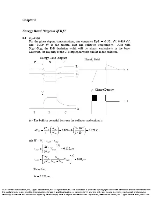
北京科技大学2013年硕士学位研究生入学考试试题============================================================================================================= 试题编号: 240 试题名称单独考试英语(共 14 页)适用专业:全校各专业单独考试考生说明:所有答案必须写在答题纸上,做在试题或草稿纸上无效。
============================================================================================================= Part I: Vocabulary (20 minutes, 10 points, 0.5 point each)Section ADirections: There are 10 incomplete sentences in this part. For each sentence there are four choices marked A., B., C. and D. Choose the ONE that best completes the sentence and mark your answer on the ANSWER SHEET.1. Psychological studies show that some people are quick-tempered .A.at heart B. on purpose C. in person D. by nature2. If a person talks about his weak points,his listener is expected to say something in the way of .A.assures B. encouragement C. persuasion D. confirmation3. He was high school and college instructors trying to teach him how to think to use the "scientific method" rather than teaching him the structure of the subject.A.put up with B. given way to C. fallen back on D. fed up with4. The film was 'Cezanne',a 50-minute on the painter and his work.A.mediation B. medication C. meditation D. metrication5. You can't work for six hours without a single break ―it's impossible!A. continuouslyB. continuallyC. frequentlyD. often6. The humour of the play was too for the young audience and they rarely laughed.A. detailedB. feebleC. subtleD. slender7. It is well known that a child does not reach emotional security a good many years after physical maturity.A.for B. during C. as long as D. until8. Man's understanding and his mastering of matter and energy his claim to superiority;provide him with the basis for enriching and deepening human experience.A.designate B. deserve C. justify D. illustrate9. They to investigate the circumstances at the time of the accident and it is now too late to prove anything.A.ignored B. intended C. neglected D. disregarded10.People that vertical flight transports would carry millions of passengers as do theairliners of today.A. convincedB. anticipatedC. resolvedD. assuredSection BDirections: In this section, there are ten sentences with one word or phrase underlined each. Choose one of the four choices marked A, B, C and D that best keeps the meaning of the sentence if it is substituted for the underlined word.11. She didn't openly attack the plan,but her opposition was implicit in her failure to say anythingin support of it.A.explicit B. obvious C. decisive D. underlying12. We will shortly be arriving in King's Cross Station. May I remind all passengers to take theirluggage with them.A.immediately B. directly C. soon D. later13. Act according to what the laws prescribe and you'll have no trouble.A.say B. impose C. decide D. define14.The matter has been gone into very thoroughly, and we find there are no grounds for theallegations.A. investigatedB. explainedC. describedD. stated15. The test comprises four sections,namely,Listening,Reading,V ocabulary and Compositionwith a time limit for each.A.consists of B. involves C. indicates D. composes of16. Being infamous for his dishonesty in business matters,the man had few friends.A.fresh B. immediate C. notorious D. famous17. Some people persist in the practice of some very old customs or traditions just because theyenjoy doing so.A.endure B. support C. stick to D. continue in18. Many local authorities realize the need to make provisions for elderly people in their housingprogrammes.A.assistance B. rooms C. conditions D. supplies19. He was very careful in whatever he did lest something unfavourable might be written into hisrecord.A.if only B. for fear that C. unless D. otherwise20. The story was given a prominent position in the front page.A.obvious B. clear C. apparent D. noticeablePart II Cloze Test(20 minutes, 10 points, 1 point each)Directions: For each blank in the following passage, choose the best answer from the choices given below. Mark your answer on the Answer Sheet by drawing with a pencil a short bar across the corresponding letter in the brackets.It is difficult to imagine what life would be like without memory. The meanings of thousands of everyday perceptions, the bases ____21____ the decisions we make, and the roots of our habits and skills are to be ____22____ in our past experience, which are brought into the present ____23____ memory.Memory can be defined as the capacity to keep ____24____ available for later use. It includes not only "remembering" things like arithmetic or historical facts, but also any change inthe way an animal typically behaves. Memory is ____25____ when a rat gives up eating grain because he has sniffed something suspicious in the grain pile. Memory is also involved when a six-year-ole child learns to swing a baseball bat.Memory ____26____ not only in humans and animals but also in some physical objects and machines. Computers, for example, contain devices for storing data for later use. It is interesting to compare the memory-storage capacity of a computer ____27____ that of a human being. The instant-access memory of a large computer may hold up to 100 000 "words"--ready for ____28____ use. An average American teenager probably recognizes the meanings of about 100 000 words of English. However, this is but a fraction of the total ____29____ of information which the teenager has stored. Consider, for example, the number of facts and places that the teenager can recognize on sight. The use of words is the basis of the advanced problem-solving intelligence of human beings. A large part of a person's memory is in terms of words and ____30____ of words.21. A. of B. to C. for D. on22. A. keep B. found C. sought D. stored23. A. by B. from C. with D. in24. A. experiences B. bases C. observations D. information25. A. called B. taken C. involved D. included26. A. exists B. appears C. affects D. seems27. A. to B. with C. against D. for28. A. progressive B. instructive C. instant D. protective29. A. deal B. number C. mount D. amount30. A. combinations B. connections C. co-ordinations D. collectionsPart III Reading Comprehension (60 minutes, 40 points)Section A (30 points, 1.5 points each)Directions:In this part there are four passages followed by questions or unfinished statements, each with four suggested answers. Choose the one you think is the best answer and mark your choice on the Answer Sheet.Passage OneQuestions 31-35 are based on the following passage:The need for solar electricity is clear. It is safe, ecologically sound, efficient, continuouslyavailable, and it has no moving parts. The basic problem with the use of solar photovoltaic devices is economics, but until recently very little progress had been made toward the development of low-cost photovoltaic devices. The larger part of research funding has been devoted to study of single-crystal silicon solar cells, despite the evidence, including that of the leading manufacturers of crystalline silicon, that the technique holds little promise. The reason for this pattern is understandable and historical. Crystalline silicon is the active element in the very successful semiconductor industry, and virtually all of the solid state devices contain silicon transistors and diodes. Crystalline silicon, however, is particularly unsuitable to terrestrial solar cells.Crystalline silicon solar cells work well and are successfully used in the space program, where cost is not an issue. While single-crystal silicon has been proven in extraterrestrial use with efficiencies as high as 18 percent, and other more expensive and scare materials such as gallium arsenide can have even higher efficiencies, costs must be reduced by a factor of more than 100 to make them practical for commercial use. Besides the fact that the starting crystalline silicon is expensive, 95 percent of it is wasted and does not appear in the final device. Recently, there have been some imaginative attempts to make polycrystalline and ribbon silicon, which are lower in cost than high-quality single crystals; but to date the efficiencies of these apparently lower-cost arrays have been unacceptably small. Moreover, these materials are cheaper only because of the introduction of disordering in crystalline semiconductors, and disorder degrades the efficiency of crystalline solar cells.This dilemma can be avoided by preparing completely disordered or amorphous materials. Amorphous materials have disordered atomic structure as compared to crystalline materials: that is, they have only short-range order rather than the long-range periodicity of crystals. The advantages of amorphous solar cells are impressive. Whereas crystals can be grown as wafers about four inches in diameter, amorphous materials can be grown over large areas in a single process. Whereas crystalline silicon must be made 200 microns thick to absorb a sufficient amount of sunlight for efficient energy conversion, only 1 micron of the proper amorphous materials is necessary. Crystalline silicon solar cells cost in excess of $100 per square foot, but amorphous films can be created at a cost of about 50 per square foot.Although many scientists were aware of the very low cost of amorphous solar cells, they felt that they could never be manufactured with the efficiencies necessary to contribute significantly to the demand for electric power. This was based on a misconception about the feature which determines efficiency. For example, it is not the conductivity of the materials in the dark which is relevant, but only the photoconductivity, that is, the conductivity in the presence of sunlight. Already, solar cells with efficiencies well above 6 percent have been developed using amorphous materials, and further research will doubtless find even less costly amorphous materials withhigher efficiencies.31. What's the major obstacle to the wide use of solar electricity?A. Solar photovoltaic devices are too expensive.B. Little research has been done to study solar cells.C. Solar electricity is neither safe nor efficient.D. The leading manufacturers only produce crystalline silicon for extraterrestrial use.32. According to the passage, which of the following is NOT true of crystalline silicon?A. It can be found in nearly all solid state devices in the form of transistors and diodes.B. It is successfully used in the space program with high efficiency.C. It is unsuitable to terrestrial solar cells as it is limited to military use.D. Its use is not economical with a high percentage wasted.33. The author's attitude toward attempts to make polycrystalline and ribbon silicon can best bedescribed as ________.A. enthusiasmB. optimismC. doubtD. disapproval34. In Para. 3, the author focuses primarily on ________.A. presenting two types of materials for solar cellsB. discussing the advantages of amorphous materials over crystalline siliconC. pointing out the feasibility of using amorphous materials in extraterrestrial programsD. outlining the specific reasons why a problem in solar cells has not yet been solved35. Which of the following was true of many scientists?A. They felt amorphous materials were too costly.B. They were doubtful whether they could develop amorphous solar cells with higherefficiencies.C. They realized that it was the conductivity in the presence of sunlight that was relevant toefficiency.D. They were optimistic about the future use of amorphous materials with higher efficiencies.Passage TwoQuestions 36-40 are based on the following passage:My hands are sweating, my face is breaking out, my heart is pounding, my temper is short. Am I having a heart attack? Am I having a nervous breakdown? No! Final exams are coming up and I am experiencing test anxiety.Is test anxiety destructive? Can we make test anxiety work for us? The answer to both of these questions is yes. Test anxiety often interferes with student performance but this same test anxiety, if channeled correctly, can help improve performance.The good side of test anxiety is that it causes us to attend to the problem. It motivates us to want to study and prepare for the exam. Without this catalyst we might never be concerned about preparing for a test. Thus, a little anxiousness shouldn't worry you. Those of us who speak publicly know that a few butterflies in the stomach just prior to a speech means that we will probably do a good job, that we will focus on our speech and block out extraneous material.However, when stress interferes with your ability to concentrate, then it has reached the destructive state. In order to lessen the destructive elements of test anxiety, the approach should be to develop improved confidence and knowledge. These two factors go hand in hand. As your knowledge of the course material increases, your confidence in your ability to succeed will increase. As your confidence increases, your anxiety will go down, allowing your knowledge to come through more efficiently. The way you prepare for a test can reduce anxiety during the test.36. Which of the following is NOT a symptom of test anxiety?A. Hands are sweating.B. Face is breaking out.C. Heart is pounding.D. Heart attack.37. According to the passage, test anxiety can benefit us in all of the following ways except thatit________.A. motivates us to make good preparation for the testB. helps us to concentrateC. can ensure us a good score in the testD. can help improve performance if channeled correctly38. Which of the following statement is TRUE about the relationship between test anxiety and confidence and knowledge?A. As your knowledge of the course material increases, your confidence in your ability tosucceed will increase.B. As your confidence increases, your anxiety will go down.C. As your anxiety increases, your knowledge will increase more efficiently.D. Both A) and B)39. What might be discussed in the following part of the article?A. Some specific recommendations for reducing test anxietyB. The negative effects of anxiety on students who take testsC. only poor students have the problem of test anxietyD. only if you are hard-working, you will not have the problem of test anxiety40. What is the best title for the passage?A. How to prepare tests?B. Knowledge and preparation for testsC. Test Anxiety: Friend or Foe?D. Is test anxiety destructive?Passage ThreeQuestions 41-45 are based on the following passage:Like her white friends Eleanor Roosevelt and Aubrey Williams, Mary Bethune believed in the fundamental commitment of the New Deal to assist the black American's struggle and in the need for blacks to assume responsibilities to help win that struggle. Unlike those of her white liberal associates, however, Bethune's ideas had evolved out of a long experience as a "race leader." Founder of a small black college in Florida, she had become widely known by 1935 as an organizer of black women's groups and as a civil and political rights activist. Deeply religious, certain of her own capabilities, she held a relatively uncluttered view of what she felt were the New Deal's and her own people's obligations to the cause of racial justice. Unafraid to speak her mind to powerful whites, including the President, or to differing black factions, she combined faith in the ultimate willingness of whites to discard their prejudice and bigotry with a strong sense of racial pride and commitment to Negro self-help.More than her liberal white friends, Bethune argued for a strong and direct black voice in initiating and shaping government policy. She pursued this in her conversations with PresidentRoosevelt, in numerous memoranda to Aubrey Williams, and in her administrative work as head of the National Youth Administration's Office of Negro Affairs. With the assistance of Williams, she was successful in having blacks selected to NY A posts at the national, state, and local levels. But she also wanted a black presence throughout the federal government. At the beginning of the war she joined other black leaders in demanding appointments to the Selective Service Board and to the Department of the Army; and she was instrumental in 1941 in securing Earl Dickerson's membership on the Fair Employment Practices Committee. By 1944, she was still making appeals for black representation "all public programs, federal, state, and local," and "in policy-making posts as well as rank and file jobs."Though recognizing the weakness in the Roosevelt administration's response to Negro needs, Mary Bethune remained in essence a black partisan champion of the New Deal during the 1930s and 1940s. Her strong advocacy of administration policies and programs was predicated on a number of factors: her assessment of the low status of black Americans during the Depression; her faith in the willingness of some liberal whites to work for the inclusion of blacks in the government's reform and recovery measures; her conviction that only massive federal aid could elevate the Negro economically; and her belief that the thirties and forties were producing a more self-aware and self-assured black population. Like a number of her white friends in government, Bethune assumed that the preservation of democracy and black people's "full integration into the benefits and the responsibilities" of American life were inextricably tied together. She was convinced that, with the help of a friendly government, a militant, aggressive "New Negro "would emerge out of the devastation of depression and war, a "New Negro" who would "save America from itself," who would lead America toward the full realization of its democratic ideas.41. What was the common belief held by Mary Bethune and her white friends?A. For blacks who wanted to achieve equality there was a long way to go.B. It was the responsibility of both government and blacks to fight for racial justice.C. Racial prejudice was too deep-rooted to overcome.D. It was the cause of blacks to struggle for equal rights.42. Which of the following was true of Mary Bethune?A. She graduated from a small black college in Florida.B. She founded a black women's group in 1935.C. She was active in civil and political rights movement.D. She was unwilling to express her views directly to powerful whites.43. Bethune talked to President Roosevelt and wrote countless letters to Aubrey William in orderto ________.A. have blacks selected to important government postsB. let them hear direct black voiceC. be appointed to the Department of the ArmyD. appeal to them to support her campaign44. The word "instrumental" (Line 8, Para. 2) is closest in meaning to ________.A. insistentB. inspirationalC. importantD. intelligent45. What was Mary Bethune's response when she realized the Roosevelt administration didn't takestrong actions to improve the Blacks' conditions?A. She lost hope in the New Deal and began to attack it.B. She continued to support the New Deal so as to win its help in return.C. She looked forward to a more friendly white government.D. She believed only a militant, aggressive black government could save blacks.Passage FourQuestions 46-50 are based on the following passage:The exclusive emphasis on economics is yielding to an appreciation of politics. After all, before free market can thrive you need political stability. Technology is still seen as a powerful tool, but one that can have harmful as well as beneficial consequences (as Osama bin Laden has brutally shown). Most important, the global trading system is becoming more democratic, with countries like India, China and Brazil demanding a voice in the shape of trade negotiations. This too could be for the best. If a few concessions and delays mean that the free-trade system will have greater legitimacy in the developing world, it is a price well worth paying.Even September 11 could be even more beneficial. In the past four months the world has seen what American political leadership and power can do when it is ambitious, energetic and internationally minded. It is time for American economic leadership to be similarly active and visionary. Treasury Secretary Paul O'Neill's speech at the forum was an interesting beginning. O'Neill talked about changing the loans-and-grants system to developing countries to help them help themselves. He talked about insisting on internal legal and political reforms. He pointed out that foreign aid rarely works. His critiques of the current system was sharp, but anyone cancriticize. The point is to fix things. He should take this opportunity to present a series of broad American initiatives that would broaden and deepen globalization.Washington should lead the developed world by responding to the legitimate demands of the developing world on trade-that means agriculture and anti-dumping. Hormats argues for a reform of the major international economic groups and institutions. A new system of effective foreign aid could have massive economic and political benefits for the whole world.In the wake of World War II, the Truman administration set up the global economic institutions that have secured and steered the world economy ever since. Throughout the cold war, America pushed for free trade as part of an overall strategy to combat communism and shore up the free world. Making globalization work better and for more people is not simply smart economics. It is a vital part of a new national-security strategy for America.46. Which of the following is more emphasized now after September 11?A. Domestic economy.B. Politics.C. National Security.D. Global unity in fighting terrorism.47. What does Hormats argue for?A. The developing countries have to help themselves.B. A new system of effective foreign aids will work well.C. The USA pushed and will push free trade world widely to combat communism.D. The foreign aids rarely work.48. What makes the author's opinion different from O'Neill's?A. The author thought that O'Neill's talk was not to the point.B. The author didn't like the talker personally.C. O'Neill should have presented what to do to improve the economic globalization.D. The author thought what O'Neill said was precise, but not workable.49. What does the author intend to say through the last paragraph?A. The Americans should follow Truman's global economic policy.B. The author suggests that the USA should have done more.C. The USA should pursue to combat the communism in economic competition.D. The Americans may live in luxurious and quiet surroundings under the conditions of theglobalization.50. The topic that best fits the passage is ___________.A. The National Security Strategy of the USAB. The Globalization of Economy and National Security Strategy of the USAC. The World Economic ForumD. International Economic GlobalizationSection B (10 points, 2 points each)Directions: Read the following passage and complete the sentences with the information from the passage in NO MORE THAN 10 words for each sentence.Starting to write is like setting out on a sea voyage. You experience certain queasiness until you get your sea legs. To get your sea legs in writing, you need a firm grasp on what you hope to accomplish in the work you plan to write. In other words, you need to discover your purpose before you can begin to write effectively. As self-evident as finding your purpose would seem to be, it is easily overlooked. Although writing is a major part of my professional life, I find I often set out to write without thinking about my purpose at all. But then, when I become queasy, I say to myself, "Just what is it I really want to do here? What do I really want to say?" In answering these questions I usually manage to get the project launched; and so the technique of asking yourself such questions is one I heartily recommend to you.Answering "What do I really want to do?" requires deciding exactly what response you want your words and ideas to evoke in those who will read them. For instance, you might want a business letter to move your correspondent to offer a job interview, or an essay to dazzle your history professor into giving you an "A". More often your aim will be less personal: you want your reader to understand your subject and to find your approach to it acceptable.In all your planning, writing, and revising, your first consideration should be how your words will affect your readers. To find out, put yourself in their place-be your own reader-and think how the words would affect you. Convincing and satisfying your readers is the whole point of writing effectively.Answering the question "What do I really want to say?" pinpoints the matter you want your readers to understand, the idea you want to convince them is valid or worth their while. In expository writing, discovering what you want to say involves finding your thesis and the means to support it. The thesis is the heart of expository writing.Although you may find the term "expository writing" unfamiliar, it describes the most familiar of all writing. It is the sort of writing found in textbooks and other works of nonfiction, in magazines, in many newspaper articles, the type of writing you are called upon to produce for college exams and business reports, the workaday, useful writing that makes the world's intellectual wheels to go around. With expository writing you expound, explain, and set forth information and ideas. It is distinguished from narrative writing, the other major type of prose, by its organization. Narrative writing, which tells a story, is structured chronologically: "and then this happened, and then that happened." Expository writing, which makes a statement, is organized to start its point, its thesis, most effectively.The essence of what you mean to get across in a given work is called the thesis. It summarizes what your reader should come to believe. It is also the organizational focus of expository writing. Conventionally, some statement of the thesis is placed toward the end of the introductory portion of a piece of expository prose and/ or somewhere in the concluding segment. Sometimes the thesis is not stated in so many words, and occasionally it is only implied; but there can be no good expository writing without it. Without a thesis, expository writing is, literally, pointless.51. What is often overlooked by people when they start to write?52. According to the passage, what is your first consideration in your writing process?53. What is the most important part of expository writing?54. What is the difference between expository writing and narrative writing?55. What is the thesis in expository writing?Part IV Translation (40 minutes, 20 points )Section ADirections:Translate the following passage from English into Chinese.The Olympic Games are a display of international goodwill. The ceremonies, with their emphasis upon both nationalism and internationalism, are a thrilling sight to see. At the start, the king or president of the country in which the Olympic Games are being held is presented. The national anthem of his country is sung. Then follows a parade of all the contestants, each bearing his country's flag and shield. This march is accompanied by a fanfare of trumpets. When the Olympic flag is raised, guns fire a salute. Doves, symbols of peace, are released. Finally the sacred fire is lit. The Olympic flame is set alight by a torch that has been carried by relay runners all the way from。
20.1%Efficient Silicon Solar Cell WithAluminum Back Surface FieldTobias Fellmeth,S.Mack,J.Bartsch,D.Erath,U.Jäger,R.Preu,F.Clement,and D.BiroAbstract—We present a standard p+pn+solar cell device exhibiting a full-area aluminum back surfacefield(BSF)and a conversion efficiency of20.1%.The front side features a shal-low emitter which has been exposed to a short oxidation step and reduces the emitter dark saturation current density j0e to 160fA/cm2on a textured surface.The front contact is formed by light-induced nickel and silver plating.Also,devices featuring screen-printed front contacts have been realized that reach a conversion efficiency of19.8%.PC1D simulations are presented in order to extract the electronic parameters of the BSF.Therefore, external quantum efficiency and reflectance have been determined for modeling the internal quantum efficiency by adapting surface recombination and lifetime of the PC1D-simulated silicon device. As a result,a recombination velocity of S BSF=283cm/s and a dark saturation current density of j BSF=274fA/cm2in the Al BSF are determined.This results in an effective diffusion length L eff=1150μm.Index Terms—Al back surfacefield(BSF),light-induced plating (LIP),screen printing,silicon solar cell.I.I NTRODUCTIONT HE ALUMINUM alloyed screen-printed(SP)andfired rear contact is still the most common approach for provid-ing the p-contact for industrial p-type silicon solar cells.This is due,on the one hand,to the cost-effective process sequence fea-turing screen printing and contactfiring and,on the other hand, to its reliability and simplicity.In the past,several authors pre-sented progress in the conversion efficiency of Al-BSF devices. Schulz et al.[1]report18.7%efficient silicon solar cells on2×2cm2float zone(FZ)material.So does Hilali et al.[2]on com-parable material by reaching19%.In2010,Hörteis et al.[3] present19.3%efficiency by utilizing a more advanced metal jet printing technique followed by light-induced plating(LIP). However,in this letter,we present a solar cell with conversion efficiency exceeding20%that features a full-area Al BSF on a 1-Ω·cm FZ-Si substrate and a cell size of2×2cm2.II.E XPERIMENTALA cross section of the device is shown in Fig.1.The front side features an emitter with a sheet resistance of∼80Ω/sq.Manuscript received April15,2011;revised May11,2011;accepted May16, 2011.Date of publication June20,2011;date of current version July27,2011. The review of this letter was arranged by Editor P.K.-L.Yu.The authors are with the Fraunhofer ISE,79110Freiburg,Germany (e-mail:tobias.fellmeth@ise.fraunhofer.de;Sebastian.Mack@ise.fhg.de; jonas.bartsch@ise.fhg.de;Denis.Erath@ise.fhg.de;ulrich.jaeger@ise.fhg.de; ralf.preu@ise.fhg.de;Florian.clement@ise.fhg.de;Daniel.biro@ise.fhg.de). Color versions of one or more of thefigures in this letter are available online at .Digital Object Identifier10.1109/LED.2011.2157656Fig.1.Representative for the solar cells presented,the cross section of the“Ni-LIP-seed–Ag-LIP device”is scheduled.(Thickness W=225μm).Thedevice is separated in regions for PC1D simulations.After a conventional POCl3diffusion,the phosphor silicateglass is heated locally by a laser where the metal front contactswill later be located.Thus,phosphorus in the glass is addi-tionally incorporated into the silicon,forming a highly n-dopedregion(n++)that is called a selective emitter[4].By applying a short thermal oxidation step at840◦C,a10-nm-thick SiO2layer is grown on both sides of the device.Due to the additional thermal budget,the surface concentrationof phosphorus decreases due to diffusion into the silicon.Thisapproach is very similar to the TOPAS concept,which waspresented in detail by Mack et al.[5].The passivation of highlyn+-doped silicon by SiO2is more effective than that by SiN x[6].Aλ/4layer of amorphous plasma-enhanced-chemical-vapor-deposited SiN x:H is segregated on top of the SiO2,reducing reflectivity and providing the essential hydrogenationof the Si−SiO2interface.By ink-jet printing an etch resist mask on the front withopenings for the contacts and dipping the cell into bufferedhydrofluoric acid,the dielectric layer is opened,exposing then++-doped emitter.Screen printing of an Al layer on the rearand subsequentfiring in a conveyor belt furnace with industrial-type belt speeds form the rear p-contact.The thin SiO2layer onthe rear is resolved duringfiring and hence does not retard theBSF formation.Nickel is deposited by LIP where the openingsin the dielectric layers have been etched.Forming gas annealat400◦C forms a Ni silicide,providing the mechanical andelectric contact.By applying a LIP step[7],silver is deposited,forming the bulkfinger generating a line resistivity of the metalgrid of2μΩ·cm.III.R ESULTSIn Table I,the IV parameters of the solar cells processedwithin this work are shown.Three different front metallizationtechniques were applied.The most advanced approach featuresa Ni seed layer and a silver-platedfinger grid reaching a conver-sion efficiency of20.1%,which we believe is the highest value 0741-3106/$26.00©2011IEEETABLE IM EASURED IV P ARAMETERS AT S TANDARD T ESTING C ONDITIONS IND EPENDENCE ON THEF RONT M ETALLIZATION.T HE F RONT E NDOF THE P ROCESS R EMAINS U NCHANGED.A LL R ESULTS W EREI NDEPENDENTLY C ONFIRMED BY F RAUNHOFER ISE C AL L ABU SING S PECTRUM AM1.5IEC60904-3E D.2(2008)Fig.2.Three Al profiles measured with the ECV technique.The profiles have been obtained for similar printing quantity belt speed.The T860curve accords to the ECV T peak=860◦C profile how it is employed in PC1D.reported for solar cells featuring an SP full-area Al alloyed rear contact on a2×2cm2sized device so far.Due to a seed layer width of30μm and afinalfinger width of50μm,an excellent short-circuit current density j sc of38.6mA/cm2is achieved. In order to reduce complexity,the Ni contact has been replaced by an SP seed layer incorporating a silver-based paste optimized for providing excellent printability and electrical contact.The lateral conductivity is also provided by Ag LIP. Due to widerfingers(80–90μm),thefill factor F F is in-creased,but j sc is decreased compared to the Ni cell;thus, the efficiencyηends up at19.8%.Within the third approach, the front metallization is only provided by screen printing a standard paste.Still,an efficiency of19.6%is achieved.IV.PC1D M ODELINGIn general,it is observed that the open-circuit voltage V oc reaches high values of nearly650mV.That is in the range of rear passivated solar cells[12].In order to perform a detailed analysis of the results achieved within this work,PC1D model-ing[8]was performed,focusing on the V oc. Electrochemical capacitance-voltage(ECV)measurements provide the Al-BSF profile.Fig.2shows two dopant profiles fired at peak temperatures of860◦C and940◦C from the boron-containing paste which has been utilized within this work.For comparison,a profile of a boron-free paste is displayed, reaching a significant lower dopant level.By extrapolation to depth=0μm,a curve is obtained,representing the“surface-effect-free”profile in the device.The tail of the ECV profileis Fig.3.Reflection and IQE as measured and simulated with PC1D for the Ni-LIP seed cell using the adapted profile shown in Fig.2.S Back denotes the recombination velocity at the BSF eutectic-layer interface.TABLE IIP ARAMETERS T HAT A RE I NCORPORATED IN THE PC1D S IMULATION A RED ISPLAYED.R EGIONS1AND2A RE D EFINED A CCORDING TOF IG.1τSRH=2.8339·10−24N accm−31.5048·f,“τSRH”=ns(1)where f denotes a free parameter which is set to2·10−6. However,this is not valid for our paste,which features boron as an additive.Thus,f needs to be reevaluated in a way that measured and simulated IQEs match.In doing so,we found that,for our paste,f=10−6fits best that results in an average lifetime in the Al-BSF region2as it is shown in Table II.In order to estimate the V oc limit of the rear side,emitter recombination is set to zero,and hence,the performance is just dominated by the rear.FELLMETH et al.:20.1%EFFICIENT SILICON SOLAR CELL WITH ALUMINUM BACK SURFACE FIELD 1103TABLE IIIS PECIFIC C ELL P ARAMETERS E XTRACTED BY PC1D S IMULATIONS A RE D ISPLAYED .j 0e I S O BTAINED F ROM S YMMETRIC S AMPLESF EATURING THE U TILIZED E MITTER .T HE U NIT OFV oc AND V oc -lim I S IN MILLIVOLTSL ·tanhWLL eff−L ·tanhWL.(3)A bulk diffusion length L of 2480μm is assumed that corresponds to the Auger and radiative limit according to Kerr and Cuevas [12].Also,the expression for j BSF is given in [11]which isj BSF =q ·n 2i ·S BSF ·N −1Base .(4)By extracting the dark saturation current density of the emit-ter j 0e =160fA/cm 2from symmetric samples,the V oc ’s of thenonmetallized and metallized cells are obtained,respectively.The V oc accords to the measured value very well if recombina-tion at the metal–emitter interface is considered.The two results underscore the approach by simulating the Al BSF with PC1D and utilizing (1)by adapting f from 2·10−6to 10−6.An effective S BSF of 283cm/s and a j BSF of 274fA/cm 2are achieved,which is an excellent value just for a full-area SP and alloyed Al rear contact.V .C ONCLUSIONA 20.1%efficient silicon solar cell has been presented ex-hibiting a standard SP aluminum rear p-contact.The front sidefeatures a laser-doped selective emitter which is contacted by Ni silicide.Also,a cell featuring an SP seed layer and a plated finger has been presented reaching an efficiency of 19.8%.By only utilizing the common one-step screen-printing technology,19.6%could be demonstrated within this work.All the cells presented feature a high open-circuit voltage of almost 650mV ,which could be explained by the rear Al dopant level,which is nearly one magnitude higher than that of a com-mon profile.PC1D simulations underscore the excellent rear side by separating the rear from the front,showing a V oc -lim =664mV of the rear side.An effective recombination velocity S BSF of 283cm/s and a dark saturation current density j BSF of 274fA/cm 2for the Al BSF on 1-Ω·cm FZ-Si are extracted.This also results in a high effective diffusion length of 1150μm,which exceeds the cell thickness by far with a factor of five.A CKNOWLEDGMENTThe author would like to thank Prof.Clement,J.Greulich,B.Thaidigsmann,R.Woehl,and M.Glatthaar for fruitful discussions.R EFERENCES[1]O.Schulz,A.Mette,M.Hermle,and S.W.Glunz,“Thermal oxidation forcrystalline silicon solar cells exceeding 19%efficiency applying industri-ally feasible process technologies,”Progr.Photovolt.Res.Appl.,vol.16,no.4,pp.317–324,Jun.2008.[2]M.M.Hilali,K.Nakayashiki,A.Ebong,and A.Rohatgi,“High-efficiency(19%)screen-printed textured cells on low-resistivity float-zone silicon with high sheet-resistance emitters,”Progr.Photovolt.Res.Appl.,vol.14,no.2,pp.135–144,Mar.2003.[3]M.Hörteis,J.Benick,J.Nekarda,A.Richter,R.Preu,and S.W.Glunz,“Fundamental studies on the front contact formation resulting in a 21%efficient silicon solar cell with printed rear and front contacts,”in Proc.35th IEEE PVSC ,USA,2010.[4]U.Jäger,M.Okanovic,M.Hörteis,A.Grohe,and R.Preu,“Selectiveemitter by laser doping from phosphosilicate glass,”in Proc.24th EU PVSEC ,Hamburg,Germany,2009,pp.1740–1743.[5]S.Mack,U.Jäger,A.Wolf,S.Nold,R.Preu,and D.Biro,“Simultane-ous front emitter and rear surface passivation by thermal oxidation—An industrially feasible approach to a 19%efficient PERC device,”in Proc.25th EU PVSEC ,Valencia,Spain,2010,pp.2218–2222.[6]M.J.Kerr,J.Schmidt,A.Cuevas,and J.H.Bultman,“Surface recombi-nation velocity of phosphorus silicon solar cell emitters passivated with plasma enhanced chemical vapor deposited silicon nitride and thermal silicon oxide,”J.Appl.Phys.,vol.89,no.7,pp.3821–3826,Apr.2001.[7]J.Bartsch,V .Radtke,C.Savio,and S.W.Glunz,“Progress in understand-ing the current paths and deposition mechanisms of light induced plating and implications for the process,”in Proc.24th EU PVSEC ,Hamburg,Germany,2009,pp.1469–1474.[8]D.A.Clugston and P.A.Basore,“PC1D version 5:32-bit solar cellmodeling on personal computers,”in Proc.26th IEEE Photovoltaic Spec.Conf.,Anaheim,Anaheim,1997,pp.207–210.[9]F.Huster and G.Schubert,“ECV doping profile measurement of alu-minum alloyed back surface fields,”in Proc.20th EU PVSEC ,Barcelona,Spain,2005,pp.1462–1465.[10]P.Altermatt,S.Steingrube,Y .Yang,C.Sprodowski,T.Dezhdar,S.Koc,B.Veith,S.Herrman,R.Bock,K.Bothe,J.Schmidt,and R.Brendel,“Highly predictive modeling of entire Si solar cells for industrial applica-tions,”in Proc.24th EU PVSEC ,Hamburg,Germany,2009,pp.901–906.[11]A.L.Fahrenbruch and R.H.Bube,Fundamentals of Solar Cells .New York:Academic,1983.[12]M.J.Kerr and A.Cuevas,“General parameterization of auger recombina-tion in crystalline silicon,”J.Appl.Phys.,vol.91,no.4,pp.2473–2480,Feb.2002.。
中国科学技术大学
博士学位论文
二次电子发射的研究和二次电子发射系数的测量
姓名:谢爱根
申请学位级别:博士
专业:核技术及应用
指导教师:裴元吉
20050501
中国科技大学博士学位论文
初级电子管壁电阻屡
图1-5(a)电子通道倍增管(b)电子通道倍增板
(5)透射式二次电子发射体
透射式二次电子发射体多是半导体和绝缘体,如KCl、MgO和si薄膜等都可制成透射式二次电子发射体。
以低密度的KCI为例,其结构示于图1.6,它是在透明的A1203(约为700A厚)基底上。
蒸镀一层700A厚的Al层作为电极,然后在低压Ar气蒸积KCI,形成20.40um低密度膜。
其密度约为正常KCI的2%。
低密度KCI是由一些条状结晶杂乱堆积而成的多孔膜层,有较大的二次电子发射系数,如=60一150,甚至更大。
相应的V一=6—9KV。
可用于磁聚焦的像增强器中,提高图像的亮度。
_Ir●
低密度KCI膜可作为摄像管的靶,如图l一6所示。
当其由图像信息的光电子从左面轰击靶时,穿透较薄的A1203和Al层进入KCI层。
由于Al电极具有正电位,KCI中产生的二次电子,或被Al电极收集,或被抑制栅网、场网收集,而空穴则向KCI靶表面运动,并在靶表面建立起图。
Diffusion lengths of silicon solar cells from luminescence images P.Würfel,a͒T.Trupke,b͒and T.PuzzerCentre of Excellence for Advanced Silicon Photovoltaics and Photonics,University of New South Wales,Sydney,NSW2052,AustraliaE.Schäffer,W.Warta,and S.W.GlunzFraunhofer Institut für Solare Energiesysteme,Heidenhofstrasse2,Freiburg79110,Germany͑Received2May2007;accepted8May2007;published online27June2007͒A method for spatially resolved measurement of the minority carrier diffusion length in siliconwafers and in silicon solar cells is introduced.The method,which is based on measuring the ratio of two luminescence images taken with two different spectralfilters,is applicable,in principle,to both photoluminescence and electroluminescence measurements and is demonstrated experimentally by electroluminescence measurements on a multicrystalline silicon solar cell.Good agreement is observed with the diffusion length distribution obtained from a spectrally resolved light beam induced current map.In contrast to the determination of diffusion lengths from one single luminescence image,the method proposed here gives absolute values of the diffusion length and,in comparison,it is much less sensitive to lateral voltage variations across the cell area as caused by local variations of the series resistance.It is also shown that measuring the ratio of two luminescence images allows distinguishing shunts or surface defects from bulk defects.©2007 American Institute of Physics.͓DOI:10.1063/1.2749201͔INTRODUCTIONCurrent methods for determining spatial variations of thediffusion length include spectral response or spectrally re-solved light beam induced current1͑LBIC͒and electrolumi-nescence imaging.2Spatially resolved spectral LBIC is amapping system and,while very accurate,it is relativelyslow.A scan on an industrial sized solar cell͑e.g.,10ϫ10cm2͒with200ϫ200pixels takes several hours.Elec-troluminescence imaging has been proposed by Fuyuki et al. as a much faster alternative technique.2,3Typical data acqui-sition times for electroluminescence images taken with a sili-con charge coupled device͑CCD͒camera with1024ϫ1024pixels are on the order of only1s.4–6However,the approach proposed by Fuyuki et al.of using a single elec-troluminescence image as a reliable and quantitative mea-surement of the diffusion length can be highly inaccurate for various reasons that will be discussed in this paper.The determination of the diffusion length from spectralresponse or from spectrally resolved LBIC is based on thefact that the contribution to the measured photocurrent ofelectron-hole pairs generated at variable distance from thep-n junction depends on the minority carrier diffusion length. Carriers do not effectively contribute to the photocurrent if the penetration depth of the incident photons is much larger than the diffusion length.In a different method for the deter-mination of the diffusion length to be discussed here,this situation is reversed.It measures luminescence signals and is based on the fact that photons generated inside the bulk of a solar cell at a point further away from the surface than their own penetration depth will be reabsorbed before reaching the surface and will therefore not contribute to the measured emission intensity.The rate of spontaneous emission of crys-talline silicon at room temperature and thus the emitted lu-minescence intensity is considerable in the wavelength range from850to1250nm,corresponding to photon penetration depths ranging from20m to several centimeters,i.e.,from much smaller than the thickness of a silicon solar cell͑typi-cally200–300m͒to much larger than that thickness.Re-stricting the measured luminescence signal to specific wave-length ranges by using suitablefilters,thus,allows information to be gained about either the total carrier density across the entire sample thickness͑long wavelength lumines-cence with long penetration depth͒or about the carrier den-sity near the front surface͑short wavelength luminescence with short penetration depth͒.The knowledge about the total carrier density and about the carrier density near the front, respectively,allows the carrier density profile and,thereby, the diffusion length to be determined,as will be shown theo-retically and experimentally below.Importantly,this method can,in principle,either be ap-plied to photoluminescence͑PL͒imaging7measurements on silicon wafers at an early stage of solar cell fabrication or to electroluminescence͑EL͒measurements carried out on fully processed solar cells.It may also be applied to other materi-als suited for solar cell fabrication.THEORYThe quantitative description of the dependence of the emission spectrum on the minority carrier diffusion length is carried out in two steps.Firstly,we describe analytically how the diffusion length affects the depth distribution of minority carriers that are injected into the base of a solar cell via an applied voltage.In a second step,we then describe how that minority carrier distribution affects the emission spectrum.a͒On leave from University of Karlsruhe.b͒Electronic mail:thorsten@trupke.deJOURNAL OF APPLIED PHYSICS101,123110͑2007͒0021-8979/2007/101͑12͒/123110/10/$23.00©2007American Institute of Physics101,123110-1The resulting relationship between the diffusion length and the emission spectrum is then used to derive a quantitative relationship between the diffusion length and the ratio of luminescence signals in two different spectral ranges.These spectral ranges are specified experimentally by the transmis-sion offilters being used for the two luminescence measure-ments.Carrier distributionWe consider the injection of electrons from the p-n junc-tion into the p-type base of a solar cell.With an applied voltage V appl,the electron concentration n e͑0͒on the p side of an abrupt p-n junction that is located at x=0is given asn e͑0͒=n i2N AexpͩeV appl kTͪ,͑1͒where n i is the intrinsic carrier concentration and N A is the doping concentration in the base.The rear surface at x=d is characterized by a surface recombination velocity S such that the electron diffusion current at the rear j e͑d͒is given byj e͑d͒=−D e dn edx͑d͒=Sn e͑d͒,͑2͒with D e the electron diffusion coefficient.Note that j e͑d͒in Eq.͑2͒is a particle current,not an electrical current.With these two boundary conditions,the electron distri-bution n e͑x͒follows from the continuity equation for elec-trons in steady state,d2n e dx2−n eL e2=0,͑3͒and isn e͑x͒=A expͩx L eͪ+B expͩ−x L eͪ,͑4͒withA=n e͑0͒1−r1−r+͑1+r͒exp͑2d/L e͒͑5͒andB=n e͑0͒1+r1+r+͑1−r͒exp͑−2d/L e͒,where L e=ͱD ee is the diffusion length and r=SL e/D e.Equations͑1͒–͑5͒allow the calculation of the minority carrier density profile as a function of the applied voltage,of the diffusion length,and of the rear surface recombination velocity.Photon emissionPhotons with energyបin the energy interval dបare generated by spontaneous radiative recombination of elec-trons and holes at a rate g␥͑x,ប͒per energy.For nondegen-erate electron and hole concentrations,the generation rate of photons by radiative recombination via band-band transitions is given by8,9g␥͑x,ប͒=␣͑ប͒͑ប͒242ប3c21exp͕͓ប−⌬͑x͔͒/kT͖−1,͑6͒where␣͑ប͒is the absorption coefficient for band to band transitions and⌬͑x͒is the local separation of the quasi-Fermi-energies.In most practical cases,the−1in the de-nominator of Eq.͑6͒can be neglected.Under the assumption of low injection conditions within the base,Eq.͑6͒can then be rewritten asg␥͑x,ប͒=␣͑ប͒͑ប͒242ប3c2expͩ−បkTͪͫn e͑x͒N A n i2ͬ.͑7͒Equation͑7͒predicts the local spectral distribution of spon-taneously emitted photons inside the sample.The same spec-tral distribution of photons would also be measured outside the sample if no reabsorption on the way to the surface oc-curred.The emitted photon current dj␥,em͑ប͒in the energy in-terval dបthat is measured outside the sample follows from integrating the contributions from the photon generation rate g␥͑x,ប͒over the thickness of the solar cell.Accounting for reabsorption with absorption coefficient␣and taking into account one reflection at the front͑R f͒and one reflection at the rear͑R r͒yieldsdj␥,emd͑ប͒͑ប͒=͓1−R f͑ប͔͒͵0d͑g␥͑x,ប͕͒exp͓−␣͑ប͒x͔+R r͑ប͒exp͓−␣͑ប͒͑2d−x͔͖͒͒dx͑8͒for the emitted photon current.Multiple reflections and, thereby,the influence of light trapping on the spectrum are neglected in Eq.͑8͒,an assumption that is justified by the selection of short passfilters used in our experiments,as discussed below.In the above treatment,it is assumed that nonradiative recombination is the dominant recombination mechanism.The generation of electron-hole pairs by the re-absorption of spontaneously emitted photons͑photon recy-cling͒is therefore neglected in the continuity equation for the electrons in Eq.͑3͒.By the same reasoning,photons emitted into directions where they are totally reflected are left out of the analysis,considering that their reabsorption will not give rise to newly emitted photons.If radiative recombination were dominant,as in many direct semiconductor materials, the electron concentration would become homogeneous through photon recycling and no information on the electron diffusion length could be gained from the shape of the emis-sion spectrum.With the electron distribution in Eq.͑4͒,the emitted pho-ton spectrum is found from Eqs.͑7͒and͑8͒by numerical integration.The resulting spectrum thus contains the infor-mation on the distribution of the electrons.Detection of emitted photonsIn previous work on luminescence imaging of silicon solar cells and silicon wafers,a silicon CCD camera has been used,providing excellent spatial resolution of1024ϫ1024pixels.On the other hand,a silicon sensor is notparticularly sensitive to the long wavelength radiation emit-ted by silicon samples.Since long wavelength radiation is poorly absorbed,it may be scattered laterally within the CCD array and may eventually be absorbed in the wrong pixel,thereby causing a smearing of the contrast.In addition,long wavelength light is also subject to light trapping within the silicon sample itself,which can lead to long wavelength photons escaping the sample far away from the point where they were generated,an effect that also leads to a smearing of the contrast.Measurements with an InGaAs camera,which is strongly absorbing across the entire spectral range in which significant luminescence from silicon occurs ͑850–1250nm ͒,would avoid the contrast smearing within the CCD itself but would still be affected by light scattering within the measured sample.In fact,that latter effect would be even more pronounced than with a silicon CCD camera,because an InGaAs sensor measures the entire long wave-length tail of the luminescence,which is most strongly af-fected by light trapping and to which a silicon CCD camera is insensitive.To reduce these problems,we restrict the detection of photons to wavelength Ͻcutoff by using a short pass filter,which blocks photons that have a penetration depth larger than the thickness of the sample.This cutoff filter will elimi-nate all long wavelength emitted light,which is enhanced by light trapping in the solar cell,which also justifies the above approach of neglecting multiple reflections within the sample in the derivation of Eq.͑8͒.The absorption length 1/␣of emitted photons as a function of the wavelength is shown for silicon at T =300K in Fig.1using absorption coefficient data determined by Weakliem and Redfield.10This depen-dence suggests a cutoff wavelength for the short pass filter cutoff between 1000and 1050nm.By using 1000and 900nm filters in the luminescence images presented in this study,the influence of lateral smearing within the sample is completely eliminated.To properly model the intensity detected by the CCD camera,its sensitivity ⌽camera ͑ប͒͑including the transmis-sion of its lens ͒and the transmission of the short pass filter T filter must be includeddj ␥,detect d ͑ប͒͑ប͒=T filter ͑ប͒⌽camera ͑ប͒dj ␥,emd ͑ប͒͑ប͒.͑9͒Figure 2shows the photon generation rate g ␥͑ប͒calculated according to Eq.͑6͒using the absorption coefficient data from Weakliem and Redfield 10multiplied by ⌽camera ͑ប͒.The peak of the rate of spontaneous emission itself ͑prior to multiplication by the sensitivity of the camera ͒is at =1140nm.However,the sensitivity of the camera decreases strongly with increasing wavelength,shifting the peak in the detected photon current to ϳ1020nm.Numerical integration of the total and of the detectable photon currents,respec-tively,shows that,depending on the exact values for ⌽camera ͑ប͒,only on the order of 5%of the total lumines-cence signal that is emitted by silicon solar cells can be cap-tured with a silicon CCD camera,which suggests that a sig-nificant improvement in the sensitivity could be achieved by using,e.g.,an InGaAs camera.Influence of the diffusion length on the detected spectrumFigure 2demonstrates the principle of how the carrier distribution influences the emitted spectrum.The two curves represent the photon fluxes that would be detected by the CCD camera for the same carrier density located either near the front or at the rear surface of a 200m thick wafer.While no difference is observed at long wavelengths,the detected photon flux at shorter wavelength is strongly re-duced for the emission from the rear surface due to reabsorp-tion of photons on their way to the front surface.The ratio of the luminescence intensities at long and short wavelengths,respectively,thus contains information about the optical path the photons have traveled within the sample and,thereby,about the carrier distribution.The spectral dependence of the detectable photon current for realistic carrier distributions was calculated according to Eqs.͑7͒–͑9͒for variable diffusion lengths.We assumed a solar cell with 300m thickness and an applied voltage of V appl =0.6V.Front and rear reflectances were assumed to be constant over the wavelength range considered.The resulting spectra were then multiplied with transmission curves ofdif-FIG.1.͑Color online ͒Absorption length of photons as a function of wave-length according to literature data for the absorption coefficient of crystal-line silicon at room temperature ͑Ref.10͒.FIG.2.͑Color online ͒Calculated emission rate multiplied by the sensitivity of a silicon CCD detector without reabsorption ͑front ͒and with reabsorption on a 200m optical path ͑rear ͒.ferent short pass filters;the latter modeled as a step function according to T filter =1for Ͻcutoff and T filter =0for ജcutoff .Figure 3shows the numerically integrated detectable photon currents for short pass filters with cutoff wavelengths ranging from 900to 1050nm ͑a curve calculated for a mea-surement with no filter is also included ͒.These data are nor-malized at large diffusion length,i.e.,they represent the sig-nals relative to what would be measured with a completely homogeneous carrier concentration;the latter pinned to n e ͑0͒by the applied voltage according to Eq.͑1͒.Importantly,the variation as a function of the diffusion length of that relative luminescence signal is different for different short pass filters being used.For the 900nm short pass filter,a strong depen-dence of the normalized luminescence signal on the diffusion length is predicted for L e Ͻ50m,and relatively little addi-tional variation for L e Ͼ100m.This is expected because the additional carriers that diffuse deeper into the cell for longer diffusion lengths do not affect the measured signal at short wavelengths due to reabsorption.In contrast,without a short pass filter,some photons with penetration depths on the order of 300m or larger are being measured ͑see Fig.2͒and,in that case,the variation of the normalized lumines-cence signal is relatively stronger for long wavelength ͑bot-tom curve in Fig.3͒.Figure 3thus shows that the short wavelength part of the luminescence spectrum that is mea-sured with a 900nm short pass filter selectively gives infor-mation about the carrier density near the front surface ͑i.e.,near the junction ͒,while measurements without filter or with a longer wavelength ͑e.g.,1000nm ͒short pass filter are more strongly affected by the carrier density profile through-out the entire device.Diffusion length from a single luminescence imageThe results from Fig.3predict a direct relationship be-tween the measured luminescence intensity and the diffusion length,which suggest that,in principle,the diffusion length distribution in a solar cell can be determined by measuring a single EL image,as was proposed and demonstrated experi-mentally by Fuyuki et al.2The graph,however,also showsthat the assumption of Fuyuki et al.of the intensity varying linearly with the diffusion length is only valid for small dif-fusion lengths.In addition,to obtain values for the diffusion length from the luminescence intensity,it is necessary to calibrate the intensity curve in Fig.3,e.g.,by comparison with the intensity of a solar cell,for which the diffusion length is known ͑e.g.,much larger than the cell thickness ͒and which is in exactly the same geometry ͑thickness,sur-face morphology,antireflection coating,voltage,etc.͒.Another,far more severe problem with the approach of Fuyuki et al.is the effect of lateral voltage variations across the cell.Due to the exponential relationship between the lo-cal excess minority carrier density and the voltage ͓Eq.͑1͔͒,a small variation of the voltage of ϳ60mV results in a very large variation of the measured luminescence intensity by a factor 10.In EL images taken with a current density equiva-lent to 1sun illumination,lateral variations in the voltage on that order can be caused,e.g.,by local variations of the series resistance or by broken metal grid fingers.11As an example,Fig.4shows an EL image of a 12.2ϫ12.2cm 2multicrystalline silicon solar cell measured with a 1000nm short pass filter mounted in front of the CCD camera.The cell was processed on industrial directionally solidified multicrystalline material using a standard industrial screen-printing process including isotexturing of the surface.A prominent feature in that image is the dark region in the bottom left section of the cell ͑dashed rectangle ͒,in which the luminescence intensity is up to a factor of 5lower than the average intensity from that cell.In a PL image taken on the same cell but with the cell operated near the maximum power point ͑image not shown here ͒,this area appears brighter than the rest of the cell,demonstrating that a locally enhanced series resistance is responsible for the reduced EL intensity from that area 11and not a reduced diffusion length.This example emphasizes the significant influence oflateralFIG.3.͑Color online ͒Normalized luminescence emission intensities ex-pected to be registered by a silicon CCD camera equipped with short pass filters with variable cutoff wavelengths of 900nm ͑dashed ͒,1000nm ͑dot-ted ͒,and 1050nm ͑dash dotted ͒as a function of the electron diffusion length in a 300m thick silicon solar cell.The bottom curve shows that dependence for a measurement without a short passfilter.FIG.4.͑Color online ͒Electroluminescence image of a multicrystalline sili-con solar cell with an area of 12.2ϫ12.2cm 2.The image is taken with a 1000nm short pass filter and with a data acquisition time of 1s ͑see text for details ͒.voltage variations on the luminescence intensity,which is completely ignored in the simplified analysis of a single lu-minescence image in terms of the diffusion length.2Diffusion length determined from the ratio of two luminescence imagesIn order to avoid the necessity of a calibration and to eliminate the effect of a laterally inhomogeneous voltage dis-tribution,we propose to measure at least two luminescence images in different wavelength ranges.The latter may be defined by two different short pass filters mounted in front of the camera objective.According to Eqs.͑6͒and ͑7͒,the lu-minescence signals in different spectral ranges will be af-fected by variations of the voltage by the same exponential factor.By dividing two luminescence signals,the effect of an inhomogeneous voltage distribution,therefore,cancels out.Figure 5shows the theoretical results for the ratio of the expected luminescence signals for various pairs of short pass filters as a function of the diffusion length L e .The division of two relative luminescence signals measured with two differ-ent short pass filters gives a number which is indicative of the absolute diffusion length and which is free from all ex-ternal effects that affect the measured intensity,such as the voltage.In Fig.5,three curves are shown for each combina-tion of filters for rear surface recombination velocities of S =0,100,and 104cm/s.It is seen that the observed ratios of luminescence intensities are little affected for S Ͻ100cm/s.In contrast,for S =104cm/s,the carrier distribution no longer varies significantly with the diffusion length L e for L e Ͼ100m,but is governed by surface recombination.In this case,the analysis of luminescence intensity ratios yields an effective diffusion length instead of the bulk diffusion length,a problem that is known for other methods as well.At least a reasonably accurate estimate of the rear surface re-combination velocity is,thus,required to analyze absolute diffusion lengths from intensity ratios.The combinations of filters used for the calculations shown in Fig.5are only some possible examples which show a strong enough depen-dence on the diffusion length.Other combinations would give similar results.EXPERIMENTSTwo dielectric short pass filters with cutoff wavelengths of 900and 1000nm,respectively,were used for this study.Our experiments revealed small nonhomogeneities across the area of both short pass filters being used,resulting in relative lateral signal variations of luminescence images of about 5%upon rotation of the filter by 90°.To reduce the influence of these filter nonhomogeneities,each luminescence image was measured by averaging four otherwise identical exposures,with the filter being rotated by 90°after each exposure.This averaging procedure was employed here in order to avoid the nonideal filter properties limiting the accuracy of the method.While causing longer total data acquisition time,this com-plication is purely a result of the nonideal filters being used here and does not represent a fundamental requirement or limitation of the method.Further work will focus on identi-fying more homogeneous dielectric filters.Figure 4shows an EL image taken with a silicon CCD camera that was cooled to −30K and with the 1000nm short pass filter.A current of 30mA/cm 2͑similar to the short cir-cuit current of the cell at 1sun illumination ͒was fed into the bus bars of the cell via two arrays of ten spring loaded con-tact pins.The contacting stage available for this study is not ideal,as the spring loaded pins and the rail they are mounted in are partially visible in the luminescence images in the vicinity of the bus bars,thereby shading part of the cell.This is only a practical and temporary limitation of our specific setup.As discussed above,the dark area on the bottom left hand side of the EL image shown in Fig.4͑dashed vertical rectangle ͒is caused by a locally enhanced series resistance.A variety of localized brighter spots are observed within that area near the grid fingers,which indicates relatively lower localized series resistance.Similar observations were re-cently reported 11and interpreted as local spots where the front grid makes better contact to the silicon than in the surrounding area of enhanced series resistance.In addition,the image shows the influence of several broken metal grid fingers ͑e.g.,black arrow in Fig.4͒which,as reported previously,4,12are characterized by dark lines along the grid finger in EL images.Two cracks on the left side of the right hand bus bar ͑dotted white arrows ͒and a large horizontal crack ͑two white arrows ͒were introduced during manual cell handling at UNSW.Neither the large horizontal crack nor the two smaller cracks were present during the spectrally re-solved LBIC measurement shown below,which was carried out at Fraunhofer ISE,Germany,prior to shipping the cell to UNSW.The three solid white arrows in the top right corner indicate two lengthy and one pointlike area of reduced EL intensity.The blurring of the EL intensity indicates a strong lateral current flow into those areas.However,from this single EL image,it is not possible to determine whether these regions correspond to local shunts or to very active recom-bination sites.The features highlighted in the EL image shown in Fig.4provide information about various fault mechanisms and electronic defects present in that solar cell.However,these features lead to strong relative variations of the ELintensityFIG.5.͑Color online ͒Calculated ratio of electroluminescence intensities,each measured with a different short pass filter.The cutoff wavelengths for the filters are indicated.Results for each signal ratio are shown for three different rear surface recombination velocities S r =1cm/s ͑solid line ͒,100cm/s ͑dotted ͒,and 104cm/s ͑dashed ͒,respectively.by up to a factor of 5,as seen in the cross sections shown on the left hand side and at the bottom of Fig.4.The cross sections represent the counts per pixel along the vertical and horizontal lines in Fig.4,respectively,on a scale from zero to 6000counts/s.These variations,which are not related to diffusion length variations,make an analysis of this indi-vidual image in terms of variations of the diffusion length impossible.A second luminescence image was measured under iden-tical operating conditions of the solar cell,but with a 900nm short pass filter replacing the 1000nm short pass filter.That second image,which is not shown here,exhibits the same features as the image shown in Fig.4.Figure 6shows the pixel by pixel ratio of the two EL images taken with the 1000nm short pass filter and with the 900nm short pass filter,respectively.The ratio was corrected for the ratio in data acquisition times for the two measurements.The com-parison of that ratio image with Fig.4shows that most of the voltage related intensity variation observed in the individual images cancels out in the ratio,as predicted theoretically.Even the quite substantial intensity variations in the indi-vidual images that are caused by high series resistance,by broken fingers,by cracks,or by significantly higher current flow into the regions near the bus bars are not visible in the intensity ratio image.The remaining intensity variations in the ratio image from Fig.6reveal the variation of the diffusion length L e .The theoretical curves shown in Fig.5were calculated for perfect short pass filters,assuming a step function for their transmission.For the conversion of the experimental lumi-nescence intensity ratio from Fig.6into a diffusion length,that theoretical relationship was calculated taking into ac-count the experimentally measured wavelength dependent transmittance of the 900and 1000nm short pass filters,re-spectively,and the wavelength dependent reflectance of the solar cell.Both the transmittance of the filters and the reflec-tance of the solar cell were measured with a Cary 500spec-trophotometer.The resulting theoretical curve is very similar to the curve in Fig.5.Because it is specific to the filters used in our experiments,the curve is not shown here.The diffusion length distribution calculated from the ra-tio of the two luminescence images ͑Fig.6͒using this theo-retical relationship is shown in Fig.7.The theoretical rela-tionships between the intensity ratio and the diffusion length ͑Fig.5͒converge towards constant values for large diffusion length.The white regions that are observed in the ratio image shown in Fig.6correspond to intensity ratios that are larger than this saturation value and are,thus,not physically mean-ingful within the above theoretical model for the carrier dis-tribution.Possible origins for these deviations will be dis-cussed further below.In the conversion of intensity ratios into diffusion length,all areas with intensity ratios greater than 37.5were converted into a diffusion length greater than 330m,which means that in Fig.7they are mappedwithFIG.6.Intensity ratio of two electroluminescence images taken under identical operating conditions of the solar cell but using two different short pass filters with cutoff wavelengths of 900and 1000nm,respectively.The large voltage related intensity variations observed in the individual images ͑see Fig.4͒are eliminated.。