1-Mbit (64K x 16) Static RAM
CY7C1021CV33
Features
?Temperature Ranges —Commercial: 0°C to 70°C —Industrial: –40°C to 85°C —Automotive-A: –40°C to 85°C —Automotive-E: –40°C to 125°C
?Pin- and function-compatible with CY7C1021BV33?High speed
—t AA = 8 ns (Commercial & Industrial)—t AA = 12 ns (Automotive)?CMOS for optimum speed/power
?Low active power: 345 mW (max.)?Automatic power-down when deselected ?Independent control of upper and lower bits
?Available in Pb-free and non Pb-free 44-pin 400-Mil SOJ 44-pin TSOP II and 48-ball FBGA packages
Functional Description [1]
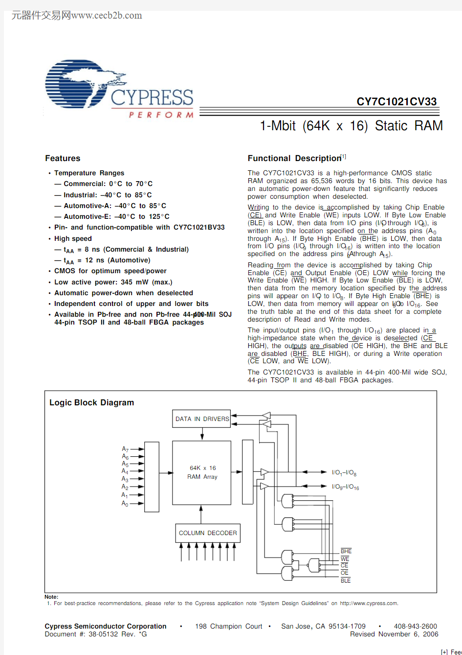
The CY7C1021CV33 is a high-performance CMOS static RAM organized as 65,536 words by 16 bits. This device has an automatic power-down feature that significantly reduces power consumption when deselected.
Writing to the device is accomplished by taking Chip Enable (CE) and Write Enable (WE) inputs LOW. If Byte Low Enable (BLE) is LOW, then data from I/O pins (I/O 1 through I/O 8), is written into the location specified on the address pins (A 0through A 15). If Byte High Enable (BHE) is LOW, then data from I/O pins (I/O 9 through I/O 16) is written into the location specified on the address pins (A 0 through A 15).
Reading from the device is accomplished by taking Chip Enable (CE) and Output Enable (OE) LOW while forcing the Write Enable (WE) HIGH. If Byte Low Enable (BLE) is LOW,then data from the memory location specified by the address pins will appear on I/O 1 to I/O 8. If Byte High Enable (BHE) is LOW, then data from memory will appear on I/O 9 to I/O 16. See the truth table at the end of this data sheet for a complete description of Read and Write modes.
The input/output pins (I/O 1 through I/O 16) are placed in a high-impedance state when the device is deselected (CE HIGH), the outputs are disabled (OE HIGH), the BHE and BLE are disabled (BHE, BLE HIGH), or during a Write operation (CE LOW, and WE LOW).
The CY7C1021CV33 is available in 44-pin 400-Mil wide SOJ,44-pin TSOP II and 48-ball FBGA packages.
Note:
1.For best-practice recommendations, please refer to the Cypress application note “System Design Guidelines” on https://www.doczj.com/doc/3917625379.html,.
Logic Block Diagram
64K x 16RAM Array
I/O 1–I/O 8R O W D E C O D E R
A 7A 6A 5A 4A 3A 0
COLUMN DECODER
A 9
A 10
A 11
A 12A 13A 14A 15
S E N S E A M P S
DATA IN DRIVERS
OE A 2A 1I/O 9–I/O 16
CE WE BLE
BHE A 8
CY7C1021CV33
Selection Guide
-8
-10-12-15Unit Maximum Access Time
8101215ns Maximum Operating Current Comm’l/Ind’l
95
90
85
80mA Automotive-A 80
mA Automotive-E
90mA Maximum CMOS Standby Current
Comm’l/Ind’l 5
5
5
5mA Automotive-A 5
mA Automotive-E
10
mA
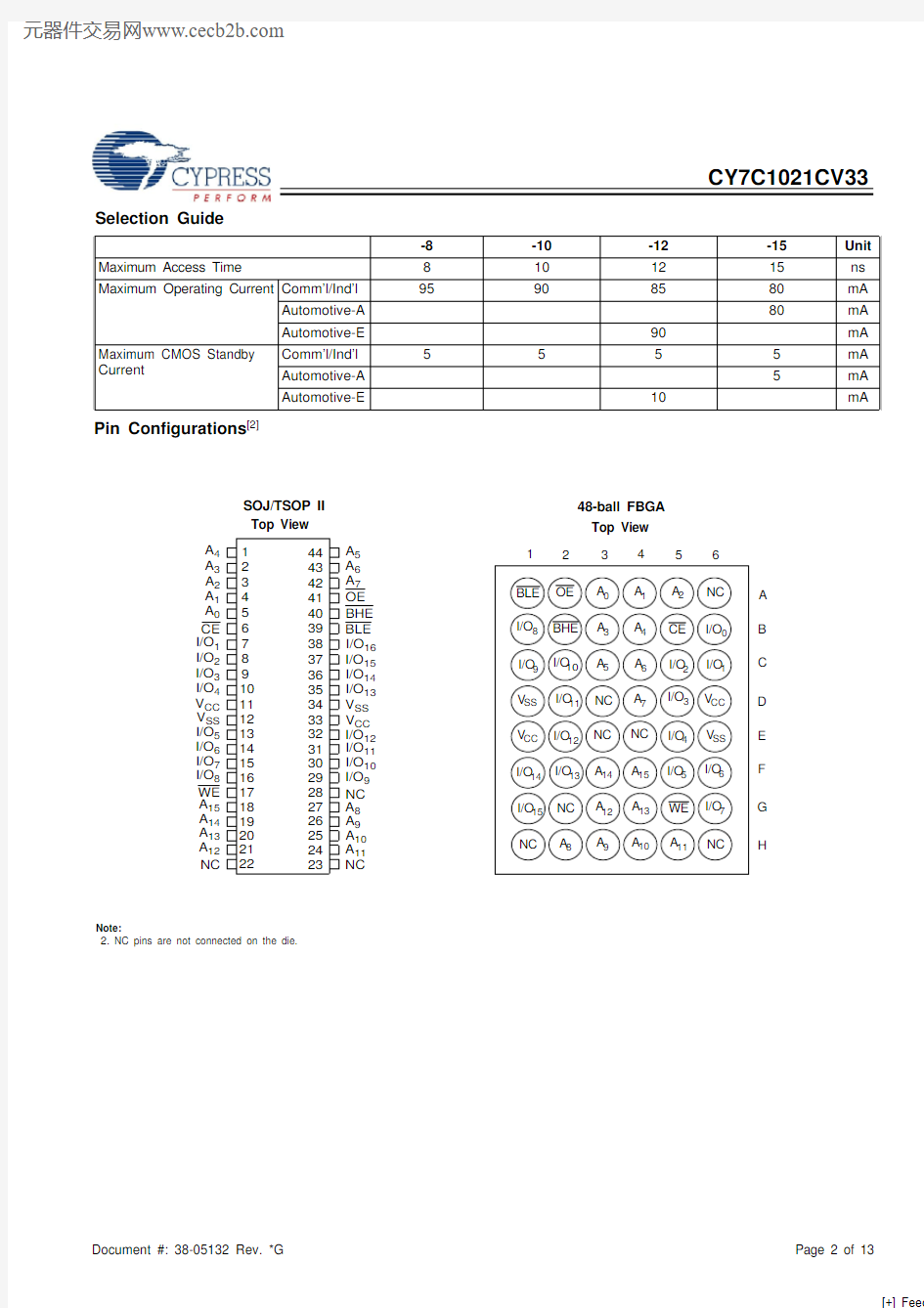
Pin Configurations [2]
WE V CC A 11
A 10
NC A 6A 0A 3CE I/O 10I/O 8I/O 9A 4A 5I/O 11I/O 13I/O 12I/O 14I/O 15V SS A 9
A 8
OE
V SS A 7I/O 0BHE NC A 2A 1BLE V CC I/O 1I/O 2I/O 3I/O 4I/O 5I/O 6I/O 7A 15A 14A 13A 12NC NC
NC
326541D E B A C F G H
NC NC 12345678911143132363534333740393812134144434216152930A 5181720192728252622
2123
2448-ball FBGA SOJ/TSOP II Top View
Top View
A 6A 7A 4A 3A 2A 1A 0A 14A 15A 8A 9A 10A 11A 12A 13NC
NC
OE BHE BLE CE WE I/O 1I/O 2I/O 3I/O 4I/O 5I/O 6I/O 7I/O 8I/O 9I/O 10I/O 11I/O 12I/O 13I/O 14I/O 15I/O 16V CC V CC V SS V SS NC 10Note:
2.NC pins are not connected on the die.
CY7C1021CV33 Pin Definitions
Pin Name SOJ, TSOP
Pin Number
BGA Pin
Number I/O Type Description
A0–A151–5, 18–21,
24–27, 42–44A3, A4, A5,
B3, B4, C3,
C4, D4, H2,
H3, H4, H5,
G3, G4, F3,
F4
Input Address Inputs used to select one of the address locations.
I/O0–I/O15[3]7–10, 13–16,
29–32, 35–38B6, C6, C5,
D5, E5, F5,
F6, G6, B1,
C1, C2, D2,
E2, F2, F1,
G1
Input/Output Bidirectional Data I/O lines. Used as input or output lines
depending on operation.
NC22, 23, 28A6, D3, E3,
E4, G2, H1,
H6
No Connect No Connects. Not connected to the die.
WE17G5Input/Control Write Enable Input, active LOW. When selected LOW, a Write is
conducted. When deselected HIGH, a Read is conducted.
CE6B5Input/Control Chip Enable Input, active LOW. When LOW, selects the chip.
When HIGH, deselects the chip.
BHE, BLE40, 39B2, A1Input/Control Byte Write Select Inputs, active LOW. BHE controls I/O16–I/O9,
BLE controls I/O8–I/O1.
OE41A2Input/Control Output Enable, active LOW. Controls the direction of the I/O pins.
When LOW, the I/O pins are allowed to behave as outputs. When
deasserted HIGH, I/O pins are tri-stated, and act as input data pins.
V SS12,34D1, E6Ground Ground for the device.Should be connected to ground of the
system.
V CC11,33D6, E1Power Supply Power Supply inputs to the device.
Note:
3.I/O1–I/O16 for SOJ/TSOP and I/O0–I/O15 for BGA packages.
CY7C1021CV33
Maximum Ratings
(Above which the useful life may be impaired. For user guide-lines, not tested.)
Storage Temperature .................................–65°C to +150°C Ambient Temperature with
Power Applied.............................................–55°C to +125°C Supply Voltage on V CC Relative to GND[4]....–0.5V to +4.6V DC Voltage Applied to Outputs
in High-Z State[4]......................................–0.5V to V CC+0.5V DC Input Voltage[4]...................................–0.5V to V CC+0.5V Current into Outputs (LOW).........................................20 mA Static Discharge Voltage.. (2001)
(per MIL-STD-883, Method 3015)
Latch-up Current......................................................>200 mA Operating Range
Range
Ambient
Temperature (T A)V CC Commercial0°C to +70°C 3.3V
± 10% Industrial–40°C to +85°C
Automotive-A–40°C to +85°C
Automotive -E–40°C to +125°C
Electrical Characteristics Over the Operating Range
Parameter Description Test Conditions
-8-10-12-15
Unit Min.Max.Min.Max.Min.Max.Min.Max.
V OH Output HIGH
Voltage V CC = Min.,
I OH = –4.0 mA
2.4 2.4 2.4 2.4V
V OL Output LOW
Voltage V CC = Min.,
I OL = 8.0 mA
0.40.40.40.4V
V IH Input HIGH
Voltage 2.0V CC
+ 0.3
2.0V CC
+ 0.3
2.0V CC
+ 0.3
2.0V CC
+ 0.3
V
V IL Input LOW
Voltage[4]
–0.30.8?0.30.8–0.30.8–0.30.8V
I IX Input Leakage
Current GND < V I < V CC Com’l/Ind’l?1+1?1+1–1+1–1+1μA Auto-A–1+1
Auto-E–12+12
I OZ Output Leakage
Current GND < V I < V CC,
Output Disabled
Com’l/Ind’l?1+1?1+1–1+1–1+1μA
Auto-A–1+1
Auto-E–12+12
I CC V CC Operating
Supply Current V CC = Max.,
I OUT = 0 mA,
f = f MAX = 1/t RC
Com’l/Ind’l95908580mA
Auto-A80mA
Auto-E90
I SB1Automatic CE
Power-Down
Current —TTL
Inputs Max. V CC,
CE > V IH
V IN > V IH or
V IN < V IL,
f = f MAX
Com’l/Ind’l15151515mA
Auto-A15
Auto-E20
I SB2Automatic CE
Power-Down
Current —CMOS
Inputs Max. V CC,
CE > V CC – 0.3V,
V IN > V CC – 0.3V,
or V IN < 0.3V,
f = 0
Com’l/Ind’l5555mA
Auto-A5
Auto-E10
Note:
4.V IL (min.) = –2.0V and V IH(max) = V CC + 0.5V for pulse durations of less than 20 ns.
CY7C1021CV33
AC Test Loads and Waveforms [6]
Notes:
5.Tested initially and after any design or process changes that may affect these parameters.
6.AC characteristics (except High-Z) for all 8-ns parts are tested using the load conditions shown in Figure (a). All other speeds are tested using the Thevenin load shown in Figure (b). High-Z characteristics are tested for all speeds using the test load shown in Figure (d).
Capacitance [5]
Parameter Description
Test Conditions
Max.Unit C IN Input Capacitance T A = 25°C, f = 1 MHz, V CC = 3.3V
8pF C OUT
Output Capacitance
8
pF
Thermal Resistance [5]
Parameter
Description
Test Conditions
SOJ TSOP II FBGA Unit ΘJA Thermal Resistance (Junction to Ambient)Test conditions follow standard test methods and procedures for
measuring thermal impedance, per EIA/JESD51
65.0676.9295.32°C/W ΘJC
Thermal Resistance (Junction to Case)
34.21
15.86
10.68
°C/W
90%10%
3.0V GND
90%10%
ALL INPUT PULSES 3.3V OUTPUT
30 pF*
* CAPACITIVE LOAD CONSISTS OF ALL COMPONENTS OF THE TEST ENVIRONMENT
(b)
R 317?
R2351?
Rise Time: 1 V/ns
Fall Time: 1 V/ns
30 pF*
OUTPUT
Z = 50?
50?
1.5V
(c)
(a) 3.3V OUTPUT
5 pF
(d)
R 317?
R2351?
8-ns devices:
10-, 12-, 15-ns devices:
High-Z characteristics:
CY7C1021CV33 Switching Characteristics Over the Operating Range[7]
Parameter Description
-8-10-12-15
Unit Min.Max.Min.Max.Min.Max.Min.Max.
Read Cycle
t power[8]V CC(typical) to the first access100100100100μs t RC Read Cycle Time8101215ns t AA Address to Data Valid8101215ns t OHA Data Hold from Address Change3333ns t ACE CE LOW to Data Valid8101215ns t DOE OE LOW to Data Valid5567ns t LZOE OE LOW to Low-Z[9]0000ns t HZOE OE HIGH to High-Z[9, 10]4567ns t LZCE CE LOW to Low-Z[9]3333ns t HZCE CE HIGH to High-Z[9, 10]4567ns t PU[11]CE LOW to Power-Up0000ns t PD[11]CE HIGH to Power-Down8101215ns t DBE Byte Enable to Data Valid5567ns t LZBE Byte Enable to Low-Z0000ns t HZBE Byte Disable to High-Z4567ns Write Cycle[12]
t WC Write Cycle Time8101215ns t SCE CE LOW to Write End78910ns t AW Address Set-up to Write End78910ns t HA Address Hold from Write End0000ns t SA Address Set-up to Write Start0000ns t PWE WE Pulse Width67810ns t SD Data Set-up to Write End5568ns t HD Data Hold from Write End0000ns t LZWE WE HIGH to Low-Z[9]3333ns t HZWE WE LOW to High-Z[9, 10]4567ns t BW Byte Enable to End of Write6789ns
Notes:
7.Test conditions assume signal transition time of 3 ns or less, timing reference levels of 1.5V, input pulse levels of 0 to 3.0V.
8.t POWER gives the minimum amount of time that the power supply should be at typical V CC values until the first memory access is performed.
9.At any given temperature and voltage condition, t HZCE is less than t LZCE, t HZOE is less than t LZOE, and t HZWE is less than t LZWE for any given device.
10.t HZOE, t HZBE, t HZCE, and t HZWE are specified with a load capacitance of 5 pF as in part (d) of AC Test Loads. Transition is measured ±500 mV from steady-state
voltage.
11.This parameter is guaranteed by design and is not tested.
12.The internal Write time of the memory is defined by the overlap of CE LOW, WE LOW and BHE/BLE LOW. CE, WE and BHE/BLE must be LOW to initiate a
Write, and the transition of these signals can terminate the Write. The input data set-up and hold timing should be referenced to the leading edge of the signal that terminates the Write.
CY7C1021CV33
Switching Waveforms
Read Cycle No. 1 (Address Transition Controlled)[13, 14]
Read Cycle No. 2 (OE Controlled)[14, 15]
Notes:
13.Device is continuously selected. OE, CE, BHE and/or BLE = V IL .14.WE is HIGH for Read cycle.
15.Address valid prior to or coincident with CE transition LOW.
PREVIOUS DATA VALID
DATA VALID
RC t AA
t OHA
t RC
ADDRESS
DATA OUT
50%
50%
DATA VALID
t RC
t ACE
t DOE
t LZOE t LZCE t PU
HIGH IMPEDANCE
t HZOE
t HZBE
t PD
t DBE
t LZBE
t HZCE HIGH IMPEDANCE
I CC I SB
OE
CE
ADDRESS
DATA OUT V CC SUPPLY BHE,BLE
CURRENT
CY7C1021CV33
Write Cycle No. 1 (CE Controlled)[16, 17]
Write Cycle No. 2 (BLE or BHE Controlled)
Notes:
16.Data I/O is high impedance if OE or BHE and/or BLE= V IH .
17.If CE goes HIGH simultaneously with WE going HIGH, the output remains in a high-impedance state.
Switching Waveforms (continued)
t HD
t SD
t SCE
t SA
t HA
t AW
t PWE
t WC
BW
t DATA I/O
ADDRESS
CE
WE
BHE,BLE
t HD
t SD
t BW
t SA
t HA
t AW
t PWE
t WC
t SCE
DATA I/O
ADDRESS
BHE,BLE
CE
WE
CY7C1021CV33
Write Cycle No. 3 (WE Controlled, LOW)
Truth Table
CE OE WE BLE BHE I/O 1–I/O 8[3]I/O 9–I/O 16[3]Mode
Power
H X X X X High-Z High-Z Power-down Standby (I SB )L
L
H
L L Data Out Data Out Read – All bits Active (I CC )L H Data Out High-Z Read – Lower bits only Active (I CC )H
L High-Z Data Out Read – Upper bits only Active (I CC )L
X
L
L L Data In Data In Write – All bits Active (I CC )L H Data In High-Z Write – Lower bits only Active (I CC )H
L High-Z Data In Write – Upper bits only Active (I CC )L H H X X High-Z High-Z Selected, Outputs Disabled Active (I CC )L
X
X
H
H
High-Z
High-Z
Selected, Outputs Disabled
Active (I CC )
Switching Waveforms (continued)
t HD
t SD t SCE
t HA
t AW
t PWE
t WC
t BW
t SA
t LZWE
t HZWE
DATA I/O
ADDRESS
CE
WE
BHE,BLE
CY7C1021CV33 Ordering Information
Speed
(ns)Ordering Code Package
Diagram Package Type
Operating
Range
8CY7C1021CV33-8VXC51-8508244-pin (400-Mil) Molded SOJ (Pb-free)Commercial CY7C1021CV33-8ZXC44-pin TSOP Type II (Pb-free)
CY7C1021CV33-8BAXC51-8509648-ball FBGA (Pb-free)
10CY7C1021CV33-10VC51-8508244-pin (400-Mil) Molded SOJ Commercial CY7C1021CV33-10VXC44-pin (400-Mil) Molded SOJ (Pb-free)
CY7C1021CV33-10ZXC51-8508744-pin TSOP Type II (Pb-free)
CY7C1021CV33-10ZI44-pin TSOP Type II Industrial
CY7C1021CV33-10ZXI44-pin TSOP Type II (Pb-free)
CY7C1021CV33-10BAXI51-8509648-ball FBGA (Pb-free)
12CY7C1021CV33-12VC51-8508244-pin (400-Mil) Molded SOJ Commercial CY7C1021CV33-12VXC44-pin (400-Mil) Molded SOJ (Pb-free)
CY7C1021CV33-12VI44-pin (400-Mil) Molded SOJ Industrial
CY7C1021CV33-12VXI44-pin (400-Mil) Molded SOJ (Pb-free)
CY7C1021CV33-12ZXC51-8508744-pin TSOP Type II (Pb-free)Commercial
CY7C1021CV33-12ZXI44-pin TSOP Type II (Pb-free)Industrial
CY7C1021CV33-12BAI51-8509648-ball FBGA Industrial
CY7C1021CV33-12BAXI48-ball FBGA (Pb-free)
CY7C1021CV33-12ZSE51-8508744-pin TSOP Type II Automotive-E CY7C1021CV33-12ZSXE44-pin TSOP Type II (Pb-free)
CY7C1021CV33-12VE51-8508244-pin (400-Mil) Molded SOJ
CY7C1021CV33-12VXE44-pin (400-Mil) Molded SOJ (Pb-free)
CY7C1021CV33-12BAE51-8509648-ball FBGA
15CY7C1021CV33-15VXC51-8508244-pin (400-Mil) Molded SOJ (Pb-free)Commercial CY7C1021CV33-15ZXC51-8508744-pin TSOP Type II (Pb-free)Commercial
CY7C1021CV33-15ZI44-pin TSOP Type II Industrial
CY7C1021CV33-15ZXI44-pin TSOP Type II (Pb-free)
CY7C1021CV33-15BAXI51-8509648-ball FBGA (Pb-free)
CY7C1021CV33-15ZSXA51-8508744-pin TSOP Type II (Pb-free)Automotive-A Please contact local sales representative regarding availability of these parts
CY7C1021CV33 Package Diagrams
44-pin (400-Mil) Molded SOJ (51-85082)
51-85082-*B
44-pin Thin Small Outline Package Type II (51-85087)
51-85087-*A
CY7C1021CV33
Document #: 38-05132 Rev. *G Page 12 of 13
All products and company names mentioned in this document are the trademarks of their respective holders.
Package Diagrams (continued)
CY7C1021CV33 Document History Page
Document Title: CY7C1021CV33, 1-Mbit (64K x 16) Static RAM
Document Number: 38-05132
REV.ECN NO.Issue
Date
Orig. of
Change Description of Change
**10947212/06/01HGK New Data Sheet
*A11504405/08/02HGK Ram7 version C4K x 16 Async
Remove “Preliminary”
*B11580806/25/02HGK I SB1 and I CC values changed
*C12041310/31/02DFP Updated BGA pin E4 to NC
*D238454See ECN RKF1) Added Automotive Specs to Data sheet
2) Added Pb-free devices in the Ordering Information
*E334398See ECN SYT Added Pb-free on page# 9 and 10
*F493565See ECN NXR Added Automotive-A operating range
Corrected typo in the Pin Definition table
Changed the description of I IX from Input Load Current to
Input Leakage Current in DC Electrical Characteristics table
Removed I OS parameter from DC Electrical Characteristics table
Updated the ordering information table
*G563963See ECN VKN Added t POWER spec in the AC Switching Characteristics table
Added footnote #8