FEATURES APPLICATIONS
DESCRIPTION
E
f
f
i
c
i
e
n
c
y
?
%
I Output Current A
O-
-
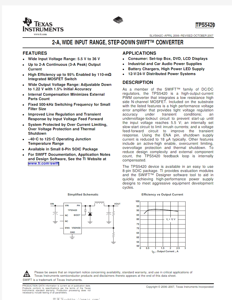
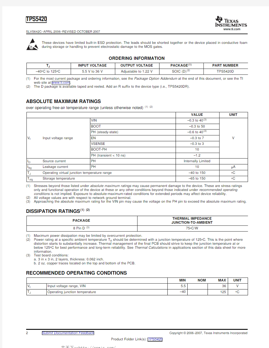
Efficiency vs Output Current
Simplified Schematic
TPS5420
SLVS642C–APRIL2006–REVISED OCTOBER2007 https://www.doczj.com/doc/3517388255.html,
2-A,WIDE INPUT RANGE,STEP-DOWN SWIFT?CONVERTER
?Consumer:Set-top Box,DVD,LCD Displays ?Wide Input Voltage Range:5.5V to36V
?Industrial and Car Audio Power Supplies
?Up to2-A Continuous(3-A Peak)Output
?Battery Chargers,High Power LED Supply Current
?12-V/24-V Distributed Power Systems
?High Efficiency up to95%Enabled by110-m?
Integrated MOSFET Switch
?Wide Output Voltage Range:Adjustable Down
to1.22V with1.5%Initial Accuracy As a member of the SWIFT?family of DC/DC
regulators,the TPS5420is a high-output-current ?Internal Compensation Minimizes External
PWM converter that integrates a low resistance high Parts Count
side N-channel MOSFET.Included on the substrate ?Fixed500-kHz Switching Frequency for Small with the listed features is a high performance voltage Filter Size error amplifier that provides tight voltage regulation
accuracy under transient conditions;an ?Improved Line Regulation and Transient
undervoltage-lockout circuit to prevent start-up until Response by Input Voltage Feed Forward
the input voltage reaches 5.5V;an internally set ?System Protected by Over Current Limiting,
slow-start circuit to limit inrush currents;and a voltage Over Voltage Protection and Thermal
feed-forward circuit to improve the transient Shutdown https://www.doczj.com/doc/3517388255.html,ing the ENA pin,shutdown supply
?–40°C to125°C Operating Junction current is reduced to18μA typically.Other features Temperature Range include an active-high enable,overcurrent limiting,
overvoltage protection and thermal shutdown.To ?Available in Small8-Pin SOIC Package
reduce design complexity and external component ?For SWIFT Documentation,Application Notes count,the TPS5420feedback loop is internally and Design Software,See the TI Website at compensated.
https://www.doczj.com/doc/3517388255.html,/swift
The TPS5420device is available in an easy to use
8-pin SOIC package.TI provides evaluation modules
and the SWIFT?Designer software tool to aid in
quickly achieving high-performance power supply
designs to meet aggressive equipment development
cycles.
Please be aware that an important notice concerning availability,standard warranty,and use in critical applications of
Texas Instruments semiconductor products and disclaimers thereto appears at the end of this data sheet.
SWIFT is a trademark of Texas Instruments.
PRODUCTION DATA information is current as of publication date.Copyright?2006–2007,Texas Instruments Incorporated Products conform to specifications per the terms of the Texas
Instruments standard warranty.Production processing does not
necessarily include testing of all parameters.
https://www.doczj.com/doc/3517388255.html,
ABSOLUTE MAXIMUM RATINGS
DISSIPATION RATINGS (1)
(2)
RECOMMENDED OPERATING CONDITIONS
TPS5420
SLVS642C–APRIL 2006–REVISED OCTOBER 2007
These devices have limited built-in ESD protection.The leads should be shorted together or the device placed in conductive foam during storage or handling to prevent electrostatic damage to the MOS gates.
ORDERING INFORMATION
T J
INPUT VOLTAGE OUTPUT VOLTAGE PACKAGE (1)PART NUMBER –40°C to 125°C 5.5V to 36V
Adjustable to 1.22V
SOIC (D)(2)
TPS5420D
(1)For the most current package and ordering information,see the Package Option Addendum at the end of this document,or see the TI web site at https://www.doczj.com/doc/3517388255.html, .
(2)
The D package is available taped and reeled.Add an R suffix to the device type (i.e.,TPS5420DR).
over operating free-air temperature range (unless otherwise noted)
(1)(2)
VALUE UNIT
VIN –0.3to 40(3)BOOT
–0.3to 50PH (steady-state)
–0.6to 40(3)V I
Input voltage range
EN –0.3to 7V
VSENSE –0.3to 3BOOT-PH
10PH (transient <10ns)
–1.2I O Source current PH Internally Limited
I lkg Leakage current PH
10μA T J Operating virtual junction temperature range
–40to 150°C T stg Storage temperature
–65to 150
°C
(1)Stresses beyond those listed under absolute maximum ratings may cause permanent damage to the device.These are stress ratings only and functional operation of the device at these or any other conditions beyond those indicated under recommended operating conditions is not implied.Exposure to absolute-maximum-rated conditions for extended periods may affect device reliability.(2)All voltage values are with respect to network ground terminal.
(3)
Approaching the absolute maximum rating for the VIN pin may cause the voltage on the PH pin to exceed the absolute maximum rating.
THERMAL IMPEDANCE PACKAGE JUNCTION-TO-AMBIENT
8Pin D
(3)
75°C/W
(1)Maximum power dissipation may be limited by overcurrent protection.
(2)
Power rating at a specific ambient temperature T A should be determined with a junction temperature of 125°C.This is the point where distortion starts to substantially increase.Thermal management of the final PCB should strive to keep the junction temperature at or below 125°C for best performance and long-term reliability.See Thermal Calculations in applications section of this data sheet for more information.
(3)
Test board conditions:
a.3in x 3in,2layers,thickness:0.062inch.
b.2oz.copper traces located on the top and bottom of the PCB.
MIN
NOM
MAX UNIT V I Input voltage range,VIN 5.536V T J
Operating junction temperature
–40
125
°C
2Submit Documentation Feedback
Copyright ?2006–2007,Texas Instruments Incorporated
Product Folder Link(s):TPS5420
https://www.doczj.com/doc/3517388255.html,
ELECTRICAL CHARACTERISTICS
TPS5420 SLVS642C–APRIL2006–REVISED OCTOBER2007
T J=–40°C to125°C,VIN=5.5V to36V(unless otherwise noted)
PARAMETER TEST CONDITIONS MIN TYP MAX UNIT SUPPLY VOLTAGE(VIN PIN)
VSENSE=2V,Not switching,PH pin
3 4.4mA
open
I Q Quiescent current
Shutdown,ENA=0V1850μA UNDERVOLTAGE LOCK OUT(UVLO)
Start threshold voltage,UVLO 5.3 5.5V
Hysteresis voltage,UVLO330mV VOLTAGE REFERENCE
T J=25°C 1.202 1.221 1.239 Voltage reference accuracy V
I O=0A–2A 1.196 1.221 1.245 OSCILLATOR
Internally set free-running frequency400500600kHz
Minimum controllable on time150200ns
Maximum duty cycle87%89%
ENABLE(ENA PIN)
Start threshold voltage,ENA 1.3V
Stop threshold voltage,ENA0.5V
Hysteresis voltage,ENA450mV
Internal slow-start time(0~100%) 6.6810ms CURRENT LIMIT
Current limit345A
Current limit hiccup time131620ms THERMAL SHUTDOWN
Thermal shutdown trip point135162°C
Thermal shutdown hysteresis14°C OUTPUT MOSFET
VIN=5.5V150
r DS(on)High side power MOSFET switch m?
VIN=10V-36V110230
Copyright?2006–2007,Texas Instruments Incorporated Submit Documentation Feedback3
Product Folder Link(s):TPS5420
https://www.doczj.com/doc/3517388255.html,
PIN
ASSIGNMENTS
BOOT NC NC VSENSE
PH VIN GND ENA
TPS5420
SLVS642C–APRIL 2006–REVISED OCTOBER 2007
D PACKAG
E (TOP VIEW)
TERMINAL FUNCTIONS
TERMINAL
DESCRIPTION
NAME NO.BOOT 1Boost capacitor for the high-side FET gate driver.Connect 0.01μF low ESR capacitor from BOOT pin to PH pin.
NC 2,3Not connected internally.
VSENSE 4Feedback voltage for the regulator.Connect to output voltage divider.
ENA 5On/off control.Below 0.5V,the device stops switching.Float the pin to enable.GND 6Ground.
Input supply voltage.Bypass VIN pin to GND pin close to device package with a high quality,low ESR ceramic VIN 7capacitor.
PH
8
Source of the high side power MOSFET.Connected to external inductor and diode.
4Submit Documentation Feedback
Copyright ?2006–2007,Texas Instruments Incorporated
Product Folder Link(s):TPS5420
https://www.doczj.com/doc/3517388255.html,
TYPICAL CHARACTERISTICS
T ?Junction Temperature ?C
J o
I O p e r a t i n g Q u i e s c e n t C u r r e n t ?m A
Q ?-50
-25025125T ?Junction Temperature ?C J o
10075
50460470530500520
510f O s c i l l a t o r F r e q u e n c y ?k H z
?480490120
180150
170
160
M i n i m u m C o n t r o l l a b l e O n T i m e ?n s
130
140
-50
-25025125
T ?Junction Temperature ?C
J o
10075
50-50
-25
25
125
T ?Junction Temperature ?C
J o
10075
50
1.22
1.23
1.225
V V o l t a g e R e f e r e n c e ?V
r e f ? 1.21
1.215
T ?Junction Temperature ?C
J o r O n -S t a t e R e s i s t a n c e ?m D S (o n )W
?8
9
8.5
t I n t e r n a l S l o w S t a r t T i m e ?m s
S S ?77.5
-50
-25
25
125
T ?Junction Temperature ?C
J o
10075
50
I S h u t d o w n C u r r e n t ?A
S D m ?25
V ?Input Voltage ?V
I 5
20
15
10
7.5
8
7.5
M i n i m u m D u t y R a t i o ?%
7
7.25
-50-25025125
T ?Junction Temperature ?C
J o 1007550TPS5420
SLVS642C–APRIL 2006–REVISED OCTOBER 2007
OSCILLATOR FREQUENCY
OPERATING QUIESCENT CURRENT
MINIMUM CONTROLLABLE ON TIME
vs
vs
vs
JUNCTION TEMPERATURE
JUNCTION TEMPERATURE
Figure 1.
Figure 2.
Figure 3.
VOLTAGE REFERENCE
ON STATE RESISTANCE
INTERNAL SLOW START TIME
vs
vs
vs
JUNCTION TEMPERATURE
JUNCTION TEMPERATURE
Figure 4.
Figure 5.
Figure 6.
MINIMUM CONTROLLABLE DUTY
SHUTDOWN QUIESCENT CURRENT
RATIO vs
vs
INPUT VOLTAGE
JUNCTION TEMPERATURE
Figure 7.Figure 8.
Copyright ?2006–2007,Texas Instruments Incorporated Submit Documentation Feedback
5
Product Folder Link(s):TPS5420
https://www.doczj.com/doc/3517388255.html,
APPLICATION INFORMATION
FUNCTIONAL BLOCK DIAGRAM
DETAILED DESCRIPTION
Oscillator Frequency
Voltage Reference
Enable (ENA)and Internal Slow Start
TPS5420
SLVS642C–APRIL 2006–REVISED OCTOBER 2007
The internal free running oscillator sets the PWM switching frequency at 500kHz.The 500kHz switching frequency allows less output inductance for the same output ripple requirement resulting in a smaller output inductor.
The voltage reference system produces a precision reference signal by scaling the output of a temperature stable bandgap circuit.The bandgap and scaling circuits are trimmed during production testing to an output of 1.221V at room temperature.
The ENA pin provides electrical on/off control of the regulator.Once the ENA pin voltage exceeds the threshold voltage,the regulator starts operation and the internal slow start begins to ramp.If the ENA pin voltage is pulled below the threshold voltage,the regulator stops switching and the internal slow start resets.Connecting the pin to ground or to any voltage less than 0.5V disables the regulator and activate the shutdown mode.The quiescent current of the TPS5420in shutdown mode is typically 18μA.
6Submit Documentation Feedback
Copyright ?2006–2007,Texas Instruments Incorporated
Product Folder Link(s):TPS5420
https://www.doczj.com/doc/3517388255.html,
Undervoltage Lockout (UVLO)
Boost Capacitor (BOOT)
Output Feedback (VSENSE)
Internal Compensation
Voltage Feed Forward
Feed Forward Gain =
VIN Ramp pk-pk
(1)
Pulse-Width-Modulation (PWM)Control
Overcurrent Limiting
TPS5420
SLVS642C–APRIL 2006–REVISED OCTOBER 2007
The ENA pin has an internal pullup current source,allowing the user to float the ENA pin.If an application requires controlling the ENA pin,use open drain or open collector output logic to interface with the pin.To limit the start-up inrush current,an internal slow start circuit is used to ramp up the reference voltage from 0V to its final value linearly.The internal slow start time is 8ms typically.The TPS5420incorporates an undervoltage lockout circuit to keep the device disabled when VIN (the input voltage)is below the UVLO start voltage threshold.During power up,internal circuits are held inactive and the internal slow start is grounded until VIN exceeds the UVLO start threshold voltage.Once the UVLO start threshold voltage is reached,the internal slow start is released and device start-up begins.The device operates until VIN falls below the UVLO stop threshold voltage.The typical hysteresis in the UVLO comparator is 330mV.Connect a 0.01μF low-ESR ceramic capacitor between the BOOT pin and PH pin.This capacitor provides the gate drive voltage for the high-side MOSFET.X7R or X5R grade dielectrics are recommended due to their stable values over temperature.The output voltage of the regulator is set by feeding back the center point voltage of an external resistor divider network to the VSENSE pin.In steady-state operation,the VSENSE pin voltage should be equal to the voltage reference 1.221V.The TPS5420implements internal compensation to simplify the regulator design.Since the TPS5420uses voltage mode control,a type 3compensation network has been designed on chip to provide a high crossover frequency and a high phase margin for good stability.See the Internal Compensation Network in the applications section for more details.The internal voltage feed forward provides a constant DC power stage gain despite any variations with the input voltage.This greatly simplifies the stability analysis and improves the transient response.Voltage feed forward varies the peak ramp voltage inversely with the input voltage so that the modulator and power stage gain are constant at the feed forward gain,i.e.
The typical feed forward gain of TPS5420is 25.The regulator employs a fixed frequency pulse-width-modulator (PWM)control method.First,the feedback voltage (VSENSE pin voltage)is compared to the constant voltage reference by the high gain error amplifier and compensation network to produce a error voltage.Then,the error voltage is compared to the ramp voltage by the PWM comparator.In this way,the error voltage magnitude is converted to a pulse width which is the duty cycle.Finally,the PWM output is fed into the gate drive circuit to control the on-time of the high-side MOSFET.Overcurrent limiting is implemented by sensing the drain-to-source voltage across the high-side MOSFET.The drain to source voltage is then compared to a voltage level representing the overcurrent threshold limit.If the drain-to-source voltage exceeds the overcurrent threshold limit,the overcurrent indicator is set true.The system will ignore the overcurrent indicator for the leading edge blanking time at the beginning of each cycle to avoid any turn-on noise glitches.
Once overcurrent indicator is set true,overcurrent limiting is triggered.The high-side MOSFET is turned off for the rest of the cycle after a propagation delay.The overcurrent limiting scheme is called cycle-by-cycle current limiting.
Copyright ?2006–2007,Texas Instruments Incorporated
Submit Documentation Feedback
7
Product Folder Link(s):TPS5420
https://www.doczj.com/doc/3517388255.html,
Overvoltage Protection
Thermal Shutdown
PCB Layout
TPS5420
SLVS642C–APRIL 2006–REVISED OCTOBER 2007
Sometimes under serious overload conditions such as short-circuit,the overcurrent runaway may still happen when using cycle-by-cycle current limiting.A second mode of current limiting is used,i.e.hiccup mode overcurrent limiting.During hiccup mode overcurrent limiting,the voltage reference is grounded and the high-side MOSFET is turned off for the hiccup time.Once the hiccup time duration is complete,the regulator restarts under control of the slow start circuit.The TPS5420has an overvoltage protection (OVP)circuit to minimize voltage overshoot when recovering from output fault conditions.The OVP circuit includes an overvoltage comparator to compare the VSENSE pin voltage and a threshold of 112.5%x VREF.Once the VSENSE pin voltage is higher than the threshold,the high-side MOSFET will be forced off.When the VSENSE pin voltage drops lower than the threshold,the high-side MOSFET will be enabled again.The TPS5420protects itself from overheating with an internal thermal shutdown circuit.If the junction temperature exceeds the thermal shutdown trip point,the voltage reference is grounded and the high-side MOSFET is turned off.The part is restarted under control of the slow start circuit automatically when the junction temperature drops 14°C below the thermal shutdown trip point.Connect a low ESR ceramic bypass capacitor to the VIN pin.Care should be taken to minimize the loop area formed by the bypass capacitor connections,the VIN pin,and the TPS5420ground pin.The best way to do this is to extend the top side ground area from under the device adjacent to the VIN trace,and place the bypass capacitor as close as possible to the VIN pin.The minimum recommended bypass capacitance is 4.7μF ceramic with a X5R or X7R dielectric.
There should be a ground area on the top layer directly underneath the IC to connect the GND pin of the device and the anode of the catch diode.The GND pin should be tied to the PCB ground by connecting it to the ground area under the device as shown in Figure 9.
The PH pin should be routed to the output inductor,catch diode and boot capacitor.Since the PH connection is the switching node,the inductor should be located close to the PH pin,and the area of the PCB conductor minimized to prevent excessive capacitive coupling.The catch diode should also be placed close to the device to minimize the output current loop area.Connect the boot capacitor between the phase node and the BOOT pin as shown.Keep the boot capacitor close to the IC and minimize the conductor trace lengths.The component placements and connections shown work well,but other connection routings may also be effective.
Connect the output filter capacitor(s)as shown between the VOUT trace and GND.It is important to keep the loop formed by the PH pin,Lout,Cout and GND as small as is practical.
Connect the VOUT trace to the VSENSE pin using the resistor divider network to set the output voltage.Do not route this trace too close to the PH trace.Due to the size of the IC package and the device pinout,the trace may need to be routed under the output capacitor.The routing may be done on an alternate layer if a trace under the output capacitor is not desired.
If the grounding scheme shown is used via a connection to a different layer to route to the ENA pin.
8Submit Documentation Feedback
Copyright ?2006–2007,Texas Instruments Incorporated
Product Folder Link(s):TPS5420
https://www.doczj.com/doc/3517388255.html,
Signal VIA
trace under the output filter capacitor or on the other layer.
TPS5420
SLVS642C–APRIL 2006–REVISED OCTOBER 2007
Figure 9.Design Layout
Copyright ?2006–2007,Texas Instruments Incorporated Submit Documentation Feedback
9
Product Folder Link(s):TPS5420
https://www.doczj.com/doc/3517388255.html,
All dimensions in inches
0.220
.
2
6
0.080
Application Circuits
TPS5420
SLVS642C–APRIL2006–REVISED OCTOBER2007
Figure10.TPS5420Land Pattern
Figure11shows the schematic for a typical TPS5420application.The TPS5420can provide up to2-A output
a nominal output voltage of5V.
A.C3=Tantalum AVX TPSD107M010R0080
Figure11.Application Circuit,10-V—35V to5-V
10Submit Documentation Feedback Copyright?2006–2007,Texas Instruments Incorporated
Product Folder Link(s):TPS5420
https://www.doczj.com/doc/3517388255.html,
Design Procedure
D V IN =
( )
I OUT(MAX)x 0.25
+ I OUT(MAX)MAX x ESR C BULK SW
x ?(2)
I CIN +I
OUT(MAX)
2(3)TPS5420
SLVS642C–APRIL 2006–REVISED OCTOBER 2007
The following design procedure can be used to select component values for the TPS5420.Alternately,the SWIFT?Designer Software may be used to generate a complete design.The SWIFT?Designer Software uses an iterative design procedure and accesses a comprehensive database of components when generating a design.This section presents a simplified discussion of the design process.
To begin the design process,a few parameters must be determined.The designer must know the following:?Input voltage range ?Output voltage ?Input ripple voltage ?Output ripple voltage ?Output current rating ?Operating frequency Design Parameters
For this design example,use the following as the input parameters:
DESIGN PARAMETER (1)
EXAMPLE VALUE Input voltage range 10V to 36V
Output voltage 5V Input ripple voltage 300mV Output ripple voltage 30mV Output current rating 2A Operating frequency
500kHz
(1)
As an additional constraint,the design is set up to be small size and low component height.
Switching Frequency
The switching frequency for the TPS5420is internally set to 500kHz.It is not possible to adjust the switching frequency.Input Capacitors
The TPS5420requires an input decoupling capacitor and,depending on the application,a bulk input capacitor.The recommended value for the decoupling capacitor is 10μF.A high quality ceramic type X5R or X7R is required.For some applications,a smaller value decoupling capacitor may be used,if the input voltage and current ripple ratings are not exceeded.The voltage rating must be greater than the maximum input voltage,including ripple.For this design,two 4.7μF capacitors,C1and C4are used to allow for smaller 1812case size to be used while maintaining a 50V rating.
This input ripple voltage can be approximated by Equation 2:
Where I OUT(MAX)is the maximum load current,f SW is the switching frequency,C I is the input capacitor value and ESR MAX is the maximum series resistance of the input capacitor.
The maximum RMS ripple current also needs to be checked.For worst case conditions,this is approximated by Equation 3:
In this example,the calculated input ripple voltage is 118mV,and the RMS ripple current is 1.0A.The maximum voltage across the input capacitors would be VIN max plus delta VIN/2.The chosen input decoupling capacitors are rated for 50V,and the ripple current capacity for each is 3A at 500kHz,providing ample margin.The actual measured input ripple voltage may be larger than the calculated value due to the output impedance of the input voltage source and parasitics associated with the layout.
Copyright ?2006–2007,Texas Instruments Incorporated
Submit Documentation Feedback
11
Product Folder Link(s):TPS5420
https://www.doczj.com/doc/3517388255.html,
L MIN=
( )
V OUT IN(MAX)OUT
x V- V
V IN(max)IND OUT SW
x K x I x F x 0.8
(4)
I L(RMS)+I 2
OUT(MAX)
)112ǒV OUTǒV IN(MAX)*V OUTǔ
V IN(MAX)L OUT F SW0.8ǔ
2
?
(5)
I L(PK)= I+
OUT(MAX)
( )
V V V
OUT IN(MAX)OUT
x-
1.6x V x L x F
IN(MAX)OUT SW(6)
TPS5420
SLVS642C–APRIL2006–REVISED OCTOBER2007
CAUTION:
The maximum ratings for voltage and current are not to be exceeded under any
circumstance.
Additionally,some bulk capacitance may be needed,especially if the TPS5420circuit is not located within approximately2inches from the input voltage source.The value for this capacitor is not critical but it should be rated to handle the maximum input voltage including ripple voltage and should filter the output so that input ripple voltage is acceptable.
Output Filter Components
Two components need to be selected for the output filter,L1and C2.Since the TPS5420is an internally compensated device,a limited range of filter component types and values can be supported.
Inductor Selection
To calculate the minimum value of the output inductor,use Equation4:
K IND is a coefficient that represents the amount of inductor ripple current relative to the maximum output current. Three things need to be considered when determining the amount of ripple current in the inductor:the peak to peak ripple current affects the output ripple voltage amplitude,the ripple current affects the peak switch current, and the amount of ripple current determines at what point the circuit becomes discontinuous.For designs using the TPS5420,K IND of0.2to0.3yields good results.Low output ripple voltages is obtained when paired with the proper output capacitor,the peak switch current is below the current limit set point,and low load currents can be sourced before discontinuous operation.
For this design example,use K IND=0.2,and the minimum inductor value is27μH.The standard value used in this design is33μH.
For the output filter inductor,it is important that the RMS current and saturation current ratings not be exceeded. The RMS inductor current can be found from Equation5:
and the peak inductor current can be determined using Equation6:
For this design,the RMS inductor current is2.002A,and the peak inductor current is2.16A.The chosen inductor is a Coilcraft MSS1260-333type.The nominal inductance is33μH.It has a saturation current rating of 2.2A and a RMS current rating of2.7A,which meets the requirements.Inductor values for use with the TPS5420are in the range of10μH to100μH.
Capacitor Selection
The important design factors for the output capacitor are dc voltage rating,ripple current rating,and equivalent series resistance(ESR).The dc voltage and ripple current ratings cannot be exceeded.The ESR is important because along with the inductor ripple current it determines the amount of output ripple voltage.The actual value of the output capacitor is not critical,but some practical limits do exist.Consider the relationship between the desired closed loop crossover frequency of the design and LC corner frequency of the output filter.Due to the
12Submit Documentation Feedback Copyright?2006–2007,Texas Instruments Incorporated
Product Folder Link(s):TPS5420
https://www.doczj.com/doc/3517388255.html,
f CO+
f LC2
85V OUT
(7)
C OUT+1
3357L OUT f CO V OUT
(8)
ESR MAX+1
2p C OUT f CO
(9)
V PP(MAX) =
( )
ESR x V V V
MAX OUT IN(MAX)OUT
x-
N C IN(MAX)OUT SW
x V x L x F x 0.8
(10)
x
I COUT(RMS)=
?12[
]
V OUT IN(MAX)OUT
x V- V
V IN(MAX)OUT SW
x L- F x 0.8 x N C
( )
(11)
TPS5420
SLVS642C–APRIL2006–REVISED OCTOBER2007
design of the internal compensation,it is recommended to keep the closed loop crossover frequency in the range 3kHz to30kHz as this frequency range has adequate phase boost to allow for stable operation.For this design example,the intended closed loop crossover frequency is between2590Hz and24kHz,and below the ESR zero of the output capacitor.Under these conditions,the closed loop crossover frequency is related to the LC corner frequency as:
and the desired output capacitor value for the output filter to:
For a desired crossover of18kHz and a33-μH inductor,the calculated value for the output capacitor is100μF. The capacitor type should be chosen so that the ESR zero is above the loop crossover.The maximum ESR is: The maximum ESR of the output capacitor also determines the amount of output ripple as specified in the initial design parameters.The output ripple voltage is the inductor ripple current times the ESR of the output filter. Check that the maximum specified ESR as listed in the capacitor data sheet results in an acceptable output ripple voltage:
Where:
ΔV PP is the desired peak-to-peak output ripple.
N C is the number of parallel output capacitors.
F SW is the switching frequency.
The minimum ESR of the output capacitor should also be considered.For a good phase margin,if the ESR is zero when the ESR is at its minimum,it should not be above the internal compensation poles at24kHz and 54kHz.
The selected output capacitor must also be rated for a voltage greater than the desired output voltage plus one half the ripple voltage.Any derating amount must also be included.The maximum RMS ripple current in the output capacitor is given by Equation11:
Where:
N C is the number of output capacitors in parallel.
F SW is the switching frequency.
For this design example,a single100-μF output capacitor is chosen for C3.The calculated RMS ripple current is 143mA and the maximum ESR required is88m?.A capacitor that meets these requirements is a AVX TPSD107M010R0080,rated at10V with a maximum ESR of80m?and a ripple current rating of1.369A.This capacitor results in a peak-to-peak output ripple of26mV using equation10.An additional small0.1-μF ceramic bypass capacitor may also used,but is not included in this design.
Other capacitor types can be used with the TPS5420,depending on the needs of the application.
Copyright?2006–2007,Texas Instruments Incorporated Submit Documentation Feedback13
Product Folder Link(s):TPS5420
https://www.doczj.com/doc/3517388255.html,
R2+R1 1.221V OUT *1.221(12)
TPS5420
SLVS642C–APRIL 2006–REVISED OCTOBER 2007
Output Voltage Setpoint
The output voltage of the TPS5420is set by a resistor divider (R1and R2)from the output to the VSENSE pin.Calculate the R2resistor value for the output voltage of 5V using Equation 12:
For any TPS5420design,start with an R1value of 10k ?.R2is then 3.24k ?.Boot Capacitor
The boot capacitor should be 0.01μF.Catch Diode
The TPS5420is designed to operate using an external catch diode between PH and GND.The selected diode
must meet the absolute maximum ratings for the application:Reverse voltage must be higher than the maximum voltage at the PH pin,which is VINMAX +0.5V.Peak current must be greater than IOUTMAX plus on half the peak-to-peak inductor current.Forward voltage drop should be small for higher efficiencies.It is important to note that the catch diode conduction time is typically longer than the high-side FET on time;therefore,the diode parameters improve the overall efficiency.Additionally,check that the device chosen is capable of dissipating the power losses.For this design,a Diodes,Inc.B340A is chosen,with a reverse voltage of 40V,forward current of 3A,and a forward voltage drop of 0.5V.Additional Circuits
Figure 12shows an application circuit using a wide input voltage range.The design parameters are similar to for the design example,with a larger value output inductor and a lower closed loop crossover frequency.
A.C3=Tantalum AVX TPSD107M010R0080
Figure 12.10-V —21-V Input to 5-V Output Application Circuit
Circuit Using Ceramic Output Filter Capacitors
Figure 13shows an application circuit using all ceramic capacitors for the input and output filters which generates from a 10-V to 24-V input.The design procedure is similar to those given for the design example,except for the selection of the output filter capacitor values and the design of the additional compensation components required to stabilize the circuit.
14Submit Documentation Feedback
Copyright ?2006–2007,Texas Instruments Incorporated
Product Folder Link(s):TPS5420
https://www.doczj.com/doc/3517388255.html,
VIN 1024 V -
L1U1C2C (MIN)O 31
2
(2x 7000) x L p O (13)F =
LC 1
2L p O O x C (EFF)?(14)TPS5420
SLVS642C–APRIL 2006–REVISED OCTOBER 2007
Figure 13.Ceramic Output Filter Capacitors Circuit
Output Filter Component Selection
Using Equation 11,the minimum inductor value is 17.9μH.A value of 18μH is chosen for this design.
When using ceramic output filer capacitors,the recommended LC resonant frequency should be no more than 7kHz.Since the output inductor is already selected at 18μH,this limits the minimum output capacitor value to:
The minimum capacitor value is calculated to be 29μF.For this circuit a larger value of capacitor yields better
transient response.Two 47μF output capacitors are used for C3and C4.It is important to note that the actual capacitance of ceramic capacitors decreases with applied voltage.In this example,the output voltage is set to 3.3V,minimizing this effect.External Compensation Network
When using ceramic output capacitors,additional circuitry is required to stabilize the closed loop system.For this circuit,the external components are R3,C5,C6,and C7.To determine the value of these components,first calculate the LC resonant frequency of the output filter:
For this example the effective resonant frequency is calculated as 4109Hz
The network composed of R1,R2,R3,C5,C6,and C7has two poles and two zeros that are used to tailor the
overall response of the feedback network to accommodate the use of the ceramic output capacitors.The pole and zero locations are given by the following equations:
Copyright ?2006–2007,Texas Instruments Incorporated Submit Documentation Feedback
15
Product Folder Link(s):TPS5420
https://www.doczj.com/doc/3517388255.html,
Fp1 = 500000 x
V O F LC
(15)Fz1 = 0.7 x F LC (16)Fz2 = 2.5 x F LC
(17)
C7 =
1
2x Fp1 x (R1 || R2)p (18)
R3 =
1
2x Fz1 x C7
p (19)C6 =
1
2x Fz2 x R1
p (20)
ADVANCED INFORMATION
Output Voltage Limitations
V OUTMAX +0.87
ǒǒV INMIN *I OMAX 0.230ǔ)V D ǔ*ǒI OMAX R L ǔ*V D
(21)
V OUTMIN +0.12
ǒǒV INMAX *I OMIN 0.110ǔ)V D ǔ*ǒI OMIN R L ǔ*V D
(22)
TPS5420
SLVS642C–APRIL 2006–REVISED OCTOBER 2007
The final pole is located at a frequency too high to be of concern.The second zero,Fz2as defined by Equation 17uses 2.5for the frequency multiplier.In some cases this may need to be slightly higher or lower.range of 2.3to 2.7work well.The values for R1and R2are fixed by the 3.3-V output voltage as calculated using Equation 12.For this design R1=10k ?and R2=5.90k ?.With Fp1=426Hz,Fz1=2708Hz and Fz2=of R3,C6and C7are determined using Equation 18,Equation 19,and Equation 20:
For this design,using the closest standard values,C7is 0.1μF,R3is 590?,and C6is 1800pF.C5is added to improve load regulation performance.It is effectively in parallel with C6in the location of the second pole frequency,so it should be small in relationship to C6.C5should be less the 1/10the value of C6.For this example,150pF works well.
For additional information on external compensation of the TPS5420or other wide voltage range SWIFT devices,see SLVA237Using TPS5410/20/30/31With Aluminum/Ceramic Output Capacitors
Due to the internal design of the TPS5420,there are both upper and lower output voltage limits for any given input voltage.The upper limit of the output voltage set point is constrained by the maximum duty cycle of 87%and is given by:
Where:
V INMIN =minimum input voltage I OMAX =maximum load current V D =catch diode forward voltage.R L =output inductor series resistance.
This equation assumes maximum on resistance for the internal high side FET.
The lower limit is constrained by the minimum controllable on time which may be as high as 200ns.The approximate minimum output voltage for a given input voltage and minimum load current is given by:
Where:
V INMAX =maximum input voltage I OMIN =minimum load current V D =catch diode forward voltage.R L =output inductor series resistance.
This equation assumes nominal on resistance for the high side FET and accounts for worst case variation of operating frequency set point.Any design operating near the operational limits of the device should be checked to assure proper functionality.
16
Submit Documentation Feedback
Copyright ?2006–2007,Texas Instruments Incorporated
Product Folder Link(s):TPS5420
https://www.doczj.com/doc/3517388255.html,
Internal Compensation Network
H(s)+
ǒ1)s
2p Fz1
ǔǒ1)s
2p Fz2
ǔ
ǒs2p Fp0ǔǒ1)s2p Fp1ǔǒ1)s2p Fp2ǔǒ1)s2p Fp3ǔ
(23)
Thermal Calculations
TPS5420 SLVS642C–APRIL2006–REVISED OCTOBER2007
The design equations given in the example circuit can be used to generate circuits using the TPS5420.These designs are based on certain assumptions,and always select output capacitors within a limited range of ESR values.If a different capacitor type is desired,it may be possible to fit one to the internal compensation of the TPS5420.Equation23gives the nominal frequency response of the internal voltage-mode type III compensation network:
Where
Fp0=2165Hz,Fz1=2170Hz,Fz2=2590Hz
Fp1=24kHz,Fp2=54kHz,Fp3=440kHz
Fp3represents the non-ideal parasitics effect.
Using this information along with the desired output voltage,feed forward gain and output filter characteristics, the closed loop transfer function can be derived.
The following formulas show how to estimate the device power dissipation under continuous conduction mode operations.They should not be used if the device is working at light loads in the discontinuous conduction mode.
Conduction Loss:Pcon=I OUT2x R DS(on)x V OUT/V IN
Switching Loss:Psw=V IN x I OUT x0.01
Quiescent Current Loss:Pq=V IN x0.01
Total Loss:Ptot=Pcon+Psw+Pq
Given T A=>Estimated Junction Temperature:T J=T A+Rth x Ptot
Given T JMAX=125°C=>Estimated Maximum Ambient Temperature:T AMAX=T JMAX–Rth x Ptot
Copyright?2006–2007,Texas Instruments Incorporated Submit Documentation Feedback17
Product Folder Link(s):TPS5420
https://www.doczj.com/doc/3517388255.html,
PERFORMANCE GRAPHS
-0.3
-0.2-0.100.1
0.20.3
0.5
1
1.5
2
2.5
3
I - Output Current -A O O u t p u t R e g u l a t i o n - %
V - Input Voltage - V
I O u t p u t R e g u l a t i o n - %
0.5
1
1.52
2.5
3
I - Output Current -A
O E f f i c i e n c y - %
t - Time = 200μs/Div
PH = 5 V/Div V = 100 mV/Div (AC Coupled)
IN t - Time - 1s / Div m PH = 5 V/Div
V = 20 mV/Div (AC Coupled)
OUT t - Time - 1s / Div
m t - Time = 5 ms/Div
V = 2 V/Div
OUT V = 10 V/Div
IN V = 2 V/Div
OUT ENA = 2 V/Div
TPS5420
SLVS642C–APRIL 2006–REVISED OCTOBER 2007
The performance graphs in Figure 14-Figure 20are applicable to the circuit in Figure 11.T A =25°C.unless otherwise specified.
Figure 14.Efficiency vs.Output
Figure 15.Output Regulation %vs.
Figure 16.Input Regulation %vs.
Current
Output Current
Input Voltage
Figure 17.Input Voltage Ripple
Figure 18.Output Voltage Ripple
Figure 19.Transient Response,Io
and PH Node,I O =3A
and PH Node,I O =3A
Step 0.5to 1.5A
Figure 20.Startup Waveform,V IN
Figure 21.Startup Waveform,ENA
and V OUT and V OUT
18Submit Documentation Feedback
Copyright ?2006–2007,Texas Instruments Incorporated
Product Folder Link(s):TPS5420
PACKAGING INFORMATION
Orderable Device
Status (1)Package Type Package Drawing
Pins Package Qty Eco Plan (2)
Lead/Ball Finish MSL Peak Temp (3)TPS5420D ACTIVE SOIC D 875Green (RoHS &no Sb/Br)CU NIPDAU Level-2-260C-1YEAR TPS5420DG4ACTIVE SOIC D 875
Green (RoHS &no Sb/Br)
CU NIPDAU Level-2-260C-1YEAR TPS5420DR ACTIVE SOIC D 82500Green (RoHS &
no Sb/Br)CU NIPDAU Level-2-260C-1YEAR TPS5420DRG4
ACTIVE
SOIC
D
8
2500Green (RoHS &
no Sb/Br)
CU NIPDAU
Level-2-260C-1YEAR
(1)
The marketing status values are defined as follows:ACTIVE:Product device recommended for new designs.
LIFEBUY:TI has announced that the device will be discontinued,and a lifetime-buy period is in effect.
NRND:Not recommended for new designs.Device is in production to support existing customers,but TI does not recommend using this part in a new design.
PREVIEW:Device has been announced but is not in production.Samples may or may not be available.OBSOLETE:TI has discontinued the production of the device.
(2)
Eco Plan -The planned eco-friendly classification:Pb-Free (RoHS),Pb-Free (RoHS Exempt),or Green (RoHS &no Sb/Br)-please check https://www.doczj.com/doc/3517388255.html,/productcontent for the latest availability information and additional product content details.TBD:The Pb-Free/Green conversion plan has not been defined.
Pb-Free (RoHS):TI's terms "Lead-Free"or "Pb-Free"mean semiconductor products that are compatible with the current RoHS requirements for all 6substances,including the requirement that lead not exceed 0.1%by weight in homogeneous materials.Where designed to be soldered at high temperatures,TI Pb-Free products are suitable for use in specified lead-free processes.
Pb-Free (RoHS Exempt):This component has a RoHS exemption for either 1)lead-based flip-chip solder bumps used between the die and package,or 2)lead-based die adhesive used between the die and leadframe.The component is otherwise considered Pb-Free (RoHS compatible)as defined above.
Green (RoHS &no Sb/Br):TI defines "Green"to mean Pb-Free (RoHS compatible),and free of Bromine (Br)and Antimony (Sb)based flame retardants (Br or Sb do not exceed 0.1%by weight in homogeneous material)
(3)
MSL,Peak Temp.--The Moisture Sensitivity Level rating according to the JEDEC industry standard classifications,and peak solder temperature.
Important Information and Disclaimer:The information provided on this page represents TI's knowledge and belief as of the date that it is provided.TI bases its knowledge and belief on information provided by third parties,and makes no representation or warranty as to the accuracy of such information.Efforts are underway to better integrate information from third parties.TI has taken and continues to take
reasonable steps to provide representative and accurate information but may not have conducted destructive testing or chemical analysis on incoming materials and chemicals.TI and TI suppliers consider certain information to be proprietary,and thus CAS numbers and other limited information may not be available for release.
In no event shall TI's liability arising out of such information exceed the total purchase price of the TI part(s)at issue in this document sold by TI to Customer on an annual basis.
OTHER QUALIFIED VERSIONS OF TPS5420:
?Automotive:
TPS5420-Q1?
Enhanced Product:TPS5420-EP NOTE:Qualified Version Definitions:
?Automotive
-Q100devices qualified for high-reliability automotive applications targeting zero defects ?Enhanced Product -Supports Defense,Aerospace and Medical Applications
PACKAGE OPTION ADDENDUM
https://www.doczj.com/doc/3517388255.html,
18-Sep-2008
TAPE AND REEL INFORMATION
*All dimensions are nominal
Device
Package Type Package Drawing Pins SPQ
Reel Diameter (mm)Reel Width W1(mm)A0(mm)B0(mm)K0(mm)P1(mm)W (mm)Pin1Quadrant TPS5420DR SOIC
D
8
2500
330.0
12.4
6.4
5.2
2.1
8.0
12.0
Q1