
?TFT COLOR LCD MODULE
NL8060BC26-17
DESCRIPTION
NL8060BC26-17 is a TFT (thin film transistor) active matrix color liquid crystal display (LCD) module comprising amorphous silicon TFT attached to each signal electrode, a driving circuit, and a backlight.
The 26 cm diagonal display area contains 800 600 pixels and can display 262144 color simultaneously.NL8060BC26-17 is the successor model of NL8060AC26-11 having enhanced viewing angle, brightness and other functions.
FEATURES
?High luminance (250 cd/m 2, typ.)
?Backlight with long-life-time lamps (two lamps per one lamp holder)? Replaceable the lamp holder (Type No.: 104LHS31)?Reversible scan direction ?6-bit digital RGB signals APPLICATIONS
?Personal computer (PC) for factory automation ?Display terminals for control system ?Monitors for process controller ?New media
Document No. MA90224 (Version 1)Date Published Feb. 1999 Printed in USA
26 cm (10.4 type), 800 600 pixels, 262144 colors,incorporated two lamps/edge-light type backlight,
wide viewing angle, high brightness
PRELIMINARY DATA SHEET
NEC Electronics Inc. 1999
? Wide viewing angle (with Retardation Film)? Data enable (DE) function
2
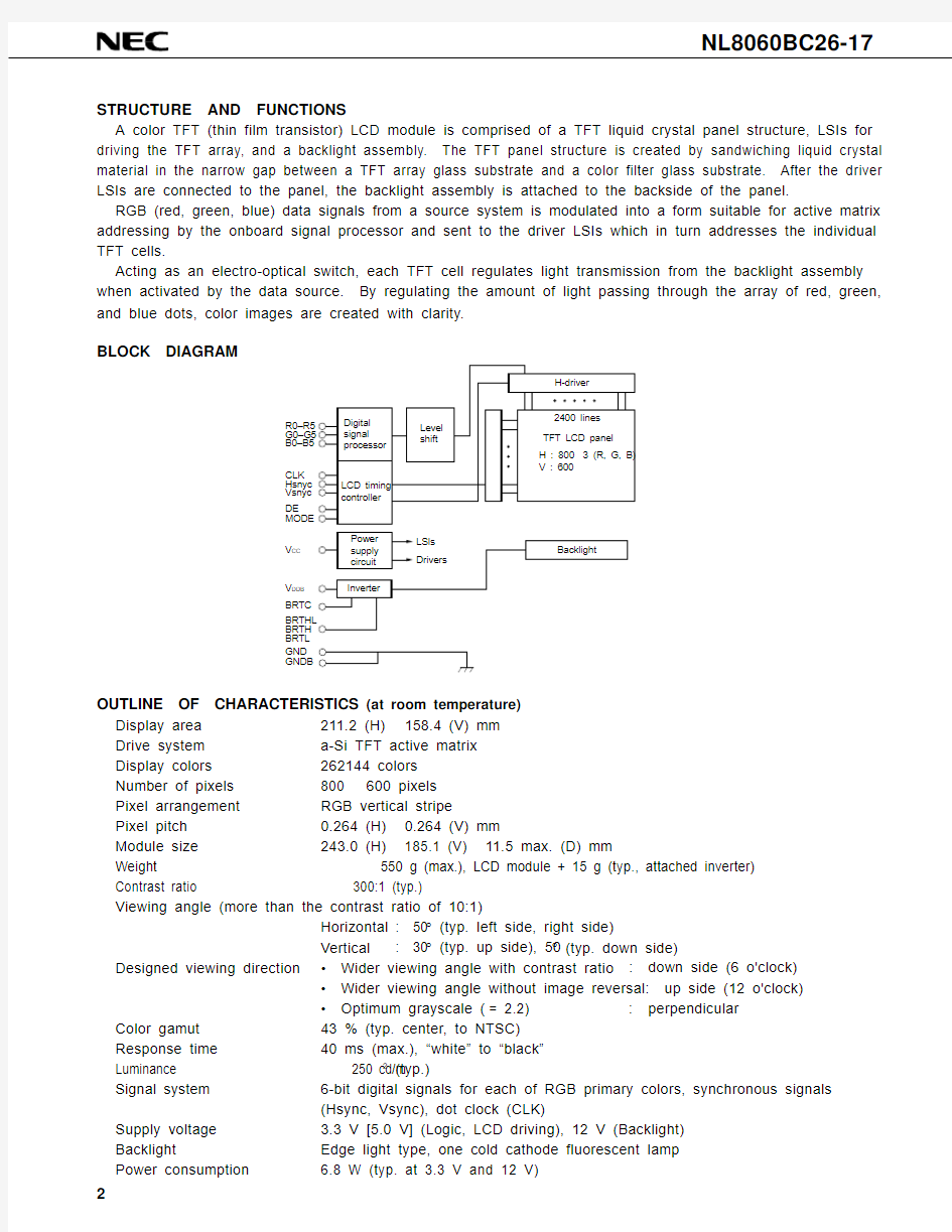
STRUCTURE AND FUNCTIONS
A color TFT (thin film transistor) LCD module is comprised of a TFT liquid crystal panel structure, LSIs for driving the TFT array, and a backlight assembly. The TFT panel structure is created by sandwiching liquid crystal material in the narrow gap between a TFT array glass substrate and a color filter glass substrate. After the driver LSIs are connected to the panel, the backlight assembly is attached to the backside of the panel.
RGB (red, green, blue) data signals from a source system is modulated into a form suitable for active matrix addressing by the onboard signal processor and sent to the driver LSIs which in turn addresses the individual TFT cells.
Acting as an electro-optical switch, each TFT cell regulates light transmission from the backlight assembly when activated by the data source. By regulating the amount of light passing through the array of red, green,and blue dots, color images are created with clarity.
BLOCK DIAGRAM
B0–B5CLK Hsnyc Vsnyc DE V CC
V DDB BRTC BRTH BRTL GND GNDB
MODE OUTLINE OF CHARACTERISTICS (at room temperature)
Display area 211.2 (H) 158.4 (V) mm Drive system a-Si TFT active matrix Display colors 262144 colors Number of pixels 800 600 pixels Pixel arrangement RGB vertical stripe Pixel pitch 0.264 (H) 0.264 (V) mm Module size 243.0 (H) 185.1 (V) 11.5 max. (D) mm
Weight 550 g (max.), LCD module + 15 g (typ., attached inverter)Contrast ratio 300:1 (typ.)
Viewing angle (more than the contrast ratio of 10:1)
Horizontal : 50° (typ. left side, right side)Vertical : 30° (typ. up side), 50° (typ. down side)
Designed viewing direction ? Wider viewing angle with contrast ratio : down side (6 o'clock)
? Wider viewing angle without image reversal: up side (12 o'clock)? Optimum grayscale ( = 2.2): perpendicular
Color gamut 43 % (typ. center, to NTSC)Response time 40 ms (max.), “white” to “black”
Luminance 250 cd/m 2
(typ.)Signal system 6-bit digital signals for each of RGB primary colors, synchronous signals
(Hsync, Vsync), dot clock (CLK)
Supply voltage 3.3 V [5.0 V] (Logic, LCD driving), 12 V (Backlight)Backlight Edge light type, one cold cathode fluorescent lamp Power consumption 6.8 W (typ. at 3.3 V and 12 V)
GENERAL SPECIFICATIONS
Item Specification Unit Module size243.0 ± 0.5 (H) 185.1 ± 0.5 (V) 11.0 max.* (D)mm
+0.7
Inverter size25.0 ± 0.5 (H) 105.0 –0.3 (V) 10.2 max. (D)mm Display area211.2 (H) 158.4 (V)mm Number of pixels800 (H) 600 (V)pixel Dot pitch0.088 (H) 0.264 (V)mm Pixel pitch0.264 (H) 0.264 (V)mm Pixel arrangement RGB (Red, Green, Blue) vertical stripe
Display colors262144color Weight480 (max.) + 20 (max., attached inverter)g
* D = 10.5 typ. ABSOLUTE MAXIMUM RATINGS
Parameter Symbol Rating Unit Remarks
Supply voltage V CC–0.3to 6.5V V I – V CC < 3.0T a = 25 C Input voltage V I–0.3to 6.5V
Storage temp.T ST–20to 60C
Operating temp.T OP0to 50C Module surface*
Humidity<= 95 % relative humidity T a<= 40 C
(No condensation)<
= 85 % relative humidity40 < T a<= 50 C
Absolute humidity shall not T a > 50 C
exceed T a = 50 C,
85 % relative humidity level
* Measured at the display area
ELECTRICAL CHARACTERISTICS
(1)Logic, LCD driving
T a = 25 C Parameter Symbol Min.Typ.Max.Unit Remarks
Supply voltage V CC 3.0 3.3 3.6V V CC = 3.3 V
(4.75)(5.0)(5.25)(V CC = 5.0 V)
Logic input “L” voltage V IL0–V CC0.3V
Logic input “H” voltage V IH V CC0.7– 5.25V
Supply current I CC–*1 310*2 550mA V CC = 3.3 V
–*1 (240)*2 (500)(V CC = 5.0 V) *1. Checker flag pattern (in EIAJ ED-2522)
*2. Theoretical maximum current pattern
3
4
(2)Backlight
T a = 25 C
Parameter
Symbol
Min.Typ.Max.Unit
Remarks
Supply current I DDB –
480550mA 250 cd/m 2Supply voltage
V DDB
11.4
12.0
12.6
Vrms
–SUPPLY VOLTAGE SEQUENCE
*1
The supply voltage for input signals should be the same as V CC .
*2
Apply V DDB within the LCD operation pe-riod. When the backlight turns on before LCD operation or the LCD operation turns
off before the backlight turns off, the dis-play may momentarily become white.*3
When the power is off, please keep whole signals (Hsync, Vsync, CLK, DE, data)low level or high impedance.
V CC Signals
V DDB
INTERFACE PIN CONNECTION
(1)Interface signals, power supply
Module side connector Mating connector
CN1 ...DF9-41P-1V (No. 1 to 41)DF9-41S-1V or DF9M-41S-1R Supplier: HIROSE ELECTRIC CO,. LTD.
or
IL-310-T41P-VF (No. 1 to 41)IL-310-T41S-VF
Supplier: Japan Aviation Electronics Industry limited (JAE)
note: Mating connectors are possible to use all parts.
Pin No.Symbol Function
1GND Ground Note 3 2DCLK Dot clock
3GND Ground Note 3 4Hsync Horizontal sync.
5Vsync Vertical sync.
6GND Ground Note 3 7GND Ground Note 3 8GND Ground Note 3 9R0Red data (LSB)
10R1Red data
11R2Red data
12GND Ground Note 3 13R3Red data
14R4Red data
15R5Red data (MSB)
16GND Ground Note 3 17GND Ground Note 3 18GND Ground Note 3 19G0Green data (LSB)
20G1Green data
21G2Green data Pin No.Symbol Function 22GND Ground Note 3 23G3Green data
24G4Green data
25G5Green data (MSB)
26GND Ground Note 3 27GND Ground Note 3 28GND Ground Note 3 29B0Blue data (LSB)
30B1Blue data
31B2Blue data
32GND Ground Note 3 33B3Blue data
34B4Blue data
35B5Blue data (MSB)
36GND Ground Note 3 37DE Data enable
38V CC Power supply Note 1 39V CC Power supply Note 1 40V CC Power supply Note 1 41MODE Timing mode select Note 2
LSB: Least Significant Bit
MSB: Most Significant Bit
Notes1.V CC: All V CC terminals should be connected to 3.3 V [5.0 V].
2.MODE:H= Fixed mode
L or open= DE mode
3.GND is connected to the frame of the LCD module.
5
6
(2)Backlight
lamp side connector Mating connector CN2 áááBHR-03VS-1
SM02 (8.0) B-BHS-TB
Supplier: J.S.T TRADING COMPANY, LTD.
Pin No.Symbol Function
1GNDB
Backlight ground 2VH High voltage terminal 3
VH
High voltage terminal
Inverter side connector 1Mating connector 1CN3 áááLZ-5P-SL-SMT
LZ-5S-SC3
Supplier: Japan Aviation Electronics Industry Limited (JAE)
Pin No.Symbol Function
Pin No.Symbol Function
1V DDB Power supply 4GNDB Backlight ground 2V DDB Power supply 5
BRTHL
Luminance select *1
3
GNDB
Backlight ground
*1:High luminance (100 %) ááá BRTHL = +5 V or open
Low luminance (60 %) ááá BRTHL = GND Inverter side connector 2Mating connector 2CM4 ááá IL-Z-3PL-SMTY
IL-Z-3S-S125C3
Supplier: Japan Aviation Electronics Industry Limited (JAE)
Pin No.Symbol Function
1BRTC Backlight ON/OFF signal *12BRTH Luminance control input *23
BRTL
Luminance control input *2
*1:TTL level
Backlight ON ááá BRTC = H or Open Backlight OFF ááá BRTC = L
*2:<1>
A way of luminance control by a variable resistor
This way works when BRTHL (No.5 pin) of CN3 is opened.
Mating variable resistor
: 10 K ±5 %
Minimum luminance (50 %): R = 0 Maximum luminance (100 %): R = 10 K
BRTH
BRTL
7
<2> A way of luminance control by a voltage
This way works when BRTHL and BRTL are opened. The range of input voltage between BRTH and GNDB is as follows.
Minimum luminance (50 %): 2.5 V Maximum luminance (100 %): <= 1.2 V
(3)Connector location
Upper side
2440
? ?? ??
8
DISPLAY COLORS vs. INPUT DATA SIGNALS
Display colors
Data signal (0: Low level, 1: High level)
R5R4R3R2R1R0
G5G4G3G2G1G0B5B4B3B2B1B0Black 000000000000000000Blue 000000000000111111Red 111111000000000000Basic colors
Magenta 111111000000111111Green 000000111111000000Cyan 000000111111111111Yellow 111111111111000000White 111111111111111111Black 000000000000000000000001000000000000Dark
00
1
00
00
00
|||Red grayscale
||||||Bright 111101000000000000111110000000000000Red 111111000000000000Black 000000000000000000000000000001000000Dark
00
00
00
1
00
|||Green grayscale
||||||Bright 000000111101000000000000111110000000Green 000000111111000000Black 000000000000000000000000000000000001Dark
00
00
00
00
1
|||Blue grayscale
||||||Bright 000000000000111101000000000000111110Blue
1
1
1
1
1
1
Note Colors are developed in combination with 6-bit signals (64 steps in grayscale) of each primary red, green,and blue color.
This process can result in up to 262144 (64 64 64) colors.
INPUT SIGNAL TIMING
(1)Input signal specifications
All of parameters should be kept in the specified range.
9
10
(2)Definition of input signal timing
Vsync
Display period DE (at DE mode)
Hsync
Display period DE (at DE mode)
Note These do not exist as signals.
11
CLK
Hsync
Vsync
CLK
Hsync
0.7 V 0.5 V 0.3 V DE
(R0-R5) 0.7 V (G0-G5) 0.5 V DATA
(B0-B5) 0.3 V 0.7 V 0.5 V 0.3 V
12
(3)Input signal timing chart
a) Fixed timing mode
(Note: Y = 0 to 599)
Hsync
R0 - R5G0 - G5B0 - B5
Hsync
Vsync
Hsync
INVALID
D (799, Y)
INVALID
R0 - R5G0 - G5B0 - B5
D (0, Y) D (1, Y)
13
b) DE mode
(Note: Y = 0 to 599)
CLK
Hsync
R0 - R5G0 - G5B0 - B5
Hsync
Vsync
DE
INVALID
D (0, Y) D (1, Y)
D (799, Y)
INVALID
R0 - R5G0 - G5B0 - B5
R0 - R5G0 - G5B0 - B5
DE
DE
14
(4)Display position
D (0, 0) D (1, 0)--------- D (X, 0)--------- D (798, 0) D (799, 0)D (0, 1)
D (1, 1)
--------- D (X, 1)
--------- D (798, 1)
D (799, 1)
------------------D (0, Y) D (1, Y)--------- D (X, Y)
--------- D (798, Y) D (799, Y)
------------------D (0, 598) D (1, 598)--------- D (X, 598)--------- D (798, 598) D (799, 598)D (0, 599)
D (1, 599)
---------
D (X, 599)
---------
D (798, 599)
D (799, 599)
---
---
---
---
---
---
---
---
---
---
---
---
---
---
GENERAL CAUTION
(1)Caution when taking out the module
1)Pick the pouch only, when taking out module from a shipping package.
(2)Cautions for handling the module
1)As the electrostatic discharges may break the LCD module, handle the LCD module with care. Peel a
protection sheet off from the LCD panel surface as slowly as possible.
2)As the LCD panel and back-light element are made from fragile glass material, impulse and pressure to the
LCD module should be avoided.
3)As the surface of polarizer is very soft and easily scratched, use a soft dry cloth without chemicals for cleaning.
4)Do not pull the interface connectors in or out while the LCD module is operating.
5)Put the module display side down on a flat horizontal plane.
6)Handle connectors and cables with care.
7)The torque to mounting screw should never exceed 0.294 N¥m (3 Kgf¥cm).
(3)Cautions for the operation
1)When the module is operating, do not lose CILK, Hsync or Vsync signals. If any one of these signals is lost,
the LCD panel would be damaged.
2)Obey the supply voltage sequence. If wrong sequence is applied, the module would be damaged. (4)Cautions for the atmosphere
1)Dew drop atmosphere should be avoided.
2)Do not store and/or operate the LCD module in a high temperature and/or humidity atmosphere. Storage
in an electro-conductive polymer packing pouch and under relatively low temperature atmosphere is recommended.
3)This module uses cold cathode fluoresent lamps. Therefore, the life time of lamps becomes short
conspicuously at low temperature.
(5)Cautions for the module characteristics
1)Do not apply fixed pattern data signal to the LCD module at product aging. Applying fixed pattern for a long
time may cause image sticking.
(6)Other cautions
1)Do not disassemble and/or re-assemble LCD module.
2)Do not re-adjust variable resistor or switch etc.
3)When returning the module for repair or etc., Please pack the module not to be broken.
We recommend to use the original shipping packages.
Liquid Crystal Display has the following specific characteristics. These are not defects or malfunctions.
The display condition of LCD module may be affected by the ambient temperature.
The LCD module uses cold cathode tubes for backlighting. Optical characteristics, like luminance or uniformity, will change during time.
Uneven brightness and/or small spots may be noticed depending on different display patterns.
15
2