SF2_Cortex_M3_Tutorial
- 格式:pdf
- 大小:3.06 MB
- 文档页数:53
第一部分准备篇第1章实验平台简介1.1EK -LM3S811开发板简介1.2主流入门Cortex M3开发平台对比第2章实验平台硬件资源详解2.1开发板原理图详解2.2开发板使用注意事项第3章RVMDK软件入门3.1RVMDK3.80A简介3.2新建RVMDK工程3.3RVMDK使用技巧3.3.1文本美化3.3.2代码编辑技巧3.3.3其他小技巧3.3.4调试技巧第4章下载与调试4.1软件仿真4.2程序下载4.3S硬件调试第5章SYSTEM文件夹介绍5.1delay文件夹代码介绍5.1.1delay_init函数5.1.2delay_μs函数5.1.3delay_ms函数5.2sys文件夹代码介绍5.2.1I/O口的位操作实现5.2.2Stm32_Clock_Init函数5.2.3Sys_Soft_Reset函数5.2.4Sys_SleepDeep函数5.2.5JTAG_Set函数5.2.6中断管理函数5.3usart文件夹介绍5.3.1USART1_IRQHandler函数5.3.2uart_init函数第二部分实践篇第6章跑马灯实验第7章按键输入实验第8章串口通信实验第9章外部中断实验第11章窗口看门狗实验第12章定时器中断实验第13章PWM输出实验第14章12864液晶显示实验第15章TFTLCD显示实验第16章RTC实时时钟实验第17章待机唤醒实验第18章ADC实验第19章内部温度传感器实验第20章DMA实验第21章I2C实验第22章SPI实验第24章无线通信实验第25章SD卡实验第26章红外遥控实验第27章DS18B20实验第28章PS/2鼠标实验第29章汉字显示实验第30章图片显示实验第31章触控USB鼠标实验第32章制作MP3播放器实验第33章综合测试实验参考文献2009年5月18日,北京讯日前,德州仪器(TI)宣布收购市场领先的基于ARM® Cortex™-M3的32位MCU供应商Luminary Micro,从而进一步壮大了其微处理器(MCU)产品阵营。

名字功能ADC带进位加法ADD加法AND 按位与(原文为逻辑与,有误——译注)。
这里的按位与和C 的”&” 功能相同ASR算术右移BIC 按位清0(把一个数跟另一个无符号数的反码按位与)CMN 负向比较(把一个数跟另一个数据的二进制补码相比较)CMP比较(比较两个数并且更新标志)CPY把一个寄存器的值拷贝到另一个寄存器中EOR近位异或LSL 逻辑左移(如无其它说明,所有移位操作都可以一次移动最多 31格——译注)LSR逻辑右移MOV 寄存器加载数据,既能用于寄存器间的传输,也能用于加载立即数MUL乘法MVN加载一个数的 NOT 值(取到逻辑反的值)NEG取二进制补码ORR按位或(原文为逻辑或,有误——译注)ROR圆圈右移SBC带借位的减法SUB减法TST 测试(执行按位与操作,并且根据结果更新 Z )REV在一个32位寄存器中反转字节序REVH 把一个32位寄存器分成两个 16位数,在每个 16位数中反转字节序REVSH 把一个32位寄存器的低 16位半字进行字节反转,然后带符号扩展到 32位SXTB带符号扩展一个字节到 32位SXTH带符号扩展一个半字到 32位UXTB无符号扩展一个字节到 32位UXTH无符号扩展一个半字到 32位16位转移指令B无条件转移B<cond>条件转移BL 转移并连接。
用于呼叫一个子程序,返回地址被存储在 LR 中BLX #im使用立即数的BLX不要在CM3 中使用CBZ 比较,如果结果为 0 就转移(只能跳到后面的指令——译注)CBNZ 比较,如果结果非 0 就转移(只能跳到后面的指令——译注)ARM CORTEX M3指令集16位数据操作指令IT If - Then16位存储器数据传送指令LDR从存储器中加载字到一个寄存器中LDRH从存储器中加载半字到一个寄存器中LDRB从存储器中加载字节到一个寄存器中LDRSH 从存储器中加载半字,再经过带符号扩展后存储一个寄存器中LDRSB 从存储器中加载字节,再经过带符号扩展后存储一个寄存器中STR把一个寄存器按字存储到存储器中STRH 把一个寄存器存器的低半字存储到存储器中STRB把一个寄存器的低字节存储到存储器中LDMIA 加载多个字,并且在加载后自增基址寄存器STMIA 存储多个字,并且在存储 后自增基址寄存器PUSH压入多个寄存器到栈中POP从栈中弹出多个值到寄存器中其它16位指令名字功能SVC系统服务调用BKPT 断点指令。
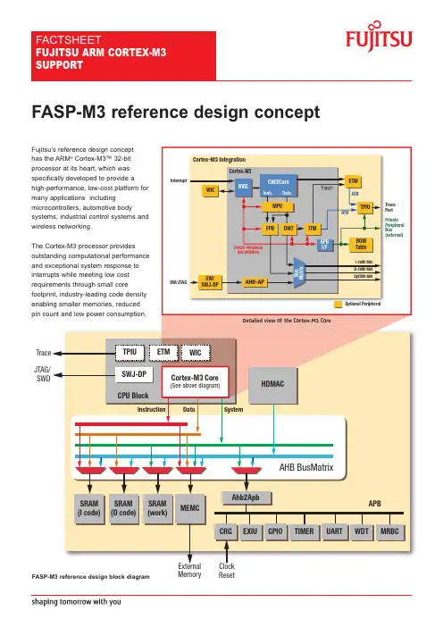
Trace JTAG/SWDAHB BusMatrixCortex-M3CoreHDMACCPU BlockSWJ-DP External Memory Clock ResetTPIU ETM WIC CRGMEMCAhb2ApbSRAM (I code)SRAM (D code)SRAM (work)EXIUGPIOTIMERUARTWDTMRBCInstruction DataSystemAPBTriggerSW/JTAGCortex-M3IntegrationCortex-M3InterruptOptional PeripheralTrace Port Private Peripheral Bus(external)CM3CoreNVICB u s M a t r i xAPB I/FWICMPUETMTPIUITMFPB DWT AHB-APSW/SWJ-DPROM TableInstr.Data.ATBATBPrivate Peripheral Bus (internal)l-code BusD-code Bus System Bus(See above diagram)Fujitsu’s reference design concept has the ARM ®Cortex-M3™32-bit processor at its heart,which was specifically developed to provide ahigh-performance,low-cost platform for many applications includingmicrocontrollers,automotive bodysystems,industrial control systems and wireless networking.The Cortex-M3processor providesoutstanding computational performance and exceptional system response to interrupts while meeting low cost requirements through small corefootprint,industry-leading code density enabling smaller memories,reduced pin count and low power consumption.FASP-M3reference design conceptDetailed view of the Cortex-M3CoreFASP-M3reference design block diagram2FSEU-A42-06SEP10FASP-M3concepts I Base platform-Only basic peripherals are implementedI Easy customisation,easy chip development-By changing the configuration of Cortex-M3-By adding or removingperipherals,replace BusMatrix -By changing interrupt signal assignment FeaturesI 32-bit high-performance and low-cost processorI ARMv7-M architecture,3-stage pipeline,Harvard architecture I 1.25DMIPS/MHzI Thumb ®-2instruction set provides enhanced levels of performance,energy efficiency,and code density I Reduced pin count for lower packaging costsI Substantial debug features-Serial Wire Debug implements debug with just 2pins-Single Wire Viewer implements single pin trace profiling I Configurable (Many optional components)-MPU,FPB,DWT,ITM,ETM,WIC,SWJ/SW-DP-Trade-off between the size and functionalities I Interrupt-NVIC (Nested Vectored Interrupt Controller)enables low latency interrupt handling -Configurable number of interrupt (default value max 240)-Configurable interrupt priority levels (max 256level supported)-16external interruptsIBus Architecture-Multi-layer AHB (ADK™3.0BusMatrix)-Use of Sparse Connect to reduce the bus confliction-AHB -APB bridge for slow peripherals IMemory System -Internal SRAM -No wait access-Separate dedicated memory for instruction and data to obtain the best performance of Cortex-M3-Work SRAM shared by Cortex-M3and other masters-128kB for instruction,32kB for data,32kB for work by default.(valiable from 4kB to 1MB)ISDRAM Interface-Support SDR SDRAM (max 128MB)IExternal ROM SRAM Interface -Support NOR and NAND flash -8chip selects.Access timing is programmable-Address and data bus are shared with SDRAM I/F for Lower cost product IEndian-Little EndianILow power modes -Sleep mode-Deep sleep mode -Stop modeDeliverables for customers I DSM of Cortex-M3and ETM -For NC-Verilog on 64-bit Linux -For Modelsim on 64-bit Linux -For VCS on 32-bit Linux I Reference Design of SoC (encrypted RTL)I Simulation environment(Testbench,Simulation script)I Boot code (initialisation of Cortex-M3and peripherals)I Documents (Specifications,User Guide,Implementation Guide)I RTL simulation model I Netlist simulation model I Timing model I Documents-Technical Reference Manual issued from ARM (open access)-Specification of Reference Design -Specifications of each Fujitsu’s IP -FASP-M3User’s GuideWords and logos marked with ®or TM are registered trademarks or trademarks of ARM Limited in the EU and other countries.Other brands and names mentioned herein may be the trademarks of their respective rmation in this fact sheet is accurate at time of publication and is subject to change without prior notice.。

SmartFusion2 MSS ARM® Cortex™-M3 ConfigurationSmartFusion2 MSS ARM® Cortex™-M3 Configuration Table of ContentsIntroduction . . . . . . . . . . . . . . . . . . . . . . . . . . . . . . . . . . . . . . . . . . . . . . . . . . . . . . . . . . . . . . . . . . . . . . 31Configuration Options. . . . . . . . . . . . . . . . . . . . . . . . . . . . . . . . . . . . . . . . . . . . . . . . . . . . . . . . . . . . . . . 4 Memory Protection Options . . . . . . . . . . . . . . . . . . . . . . . . . . . . . . . . . . . . . . . . . . . . . . . . . . . . . . . . . . . . . . . . . . . 4 Sys Tick Timer . . . . . . . . . . . . . . . . . . . . . . . . . . . . . . . . . . . . . . . . . . . . . . . . . . . . . . . . . . . . . . . . . . . . . . . . . . . . . 4 Events . . . . . . . . . . . . . . . . . . . . . . . . . . . . . . . . . . . . . . . . . . . . . . . . . . . . . . . . . . . . . . . . . . . . . . . . . . . . . . . . . . . 4 System Power Management . . . . . . . . . . . . . . . . . . . . . . . . . . . . . . . . . . . . . . . . . . . . . . . . . . . . . . . . . . . . . . . . . . 5 Trace Port Interface Unit (TPIU) . . . . . . . . . . . . . . . . . . . . . . . . . . . . . . . . . . . . . . . . . . . . . . . . . . . . . . . . . . . . . . . 52Port Description . . . . . . . . . . . . . . . . . . . . . . . . . . . . . . . . . . . . . . . . . . . . . . . . . . . . . . . . . . . . . . . . . . . 6A Product Support. . . . . . . . . . . . . . . . . . . . . . . . . . . . . . . . . . . . . . . . . . . . . . . . . . . . . . . . . . . . . . . . . . . 7Customer Service . . . . . . . . . . . . . . . . . . . . . . . . . . . . . . . . . . . . . . . . . . . . . . . . . . . . . . . . . . . . . . . . . . . . . . . . . . 7 Customer Technical Support Center . . . . . . . . . . . . . . . . . . . . . . . . . . . . . . . . . . . . . . . . . . . . . . . . . . . . . . . . . . . . 7 Technical Support . . . . . . . . . . . . . . . . . . . . . . . . . . . . . . . . . . . . . . . . . . . . . . . . . . . . . . . . . . . . . . . . . . . . . . . . . . 7 Website . . . . . . . . . . . . . . . . . . . . . . . . . . . . . . . . . . . . . . . . . . . . . . . . . . . . . . . . . . . . . . . . . . . . . . . . . . . . . . . . . . 7 Contacting the Customer Technical Support Center . . . . . . . . . . . . . . . . . . . . . . . . . . . . . . . . . . . . . . . . . . . . . . . . 7 ITAR Technical Support . . . . . . . . . . . . . . . . . . . . . . . . . . . . . . . . . . . . . . . . . . . . . . . . . . . . . . . . . . . . . . . . . . . . . . 8IntroductionThe ARM® Cortex™-M3 offers configurable features as well as available signals at the FPGA fabricinterface.The values entered in the configurator will be exported into the programming files for programming of theflash bits that control this functionality. The flash bits are loaded in the system registers at power up (orwhen the DEVRST_N external pad is asserted/de-asserted).For complete details about the ARM® Cortex-M3 feature set offered in the SmartFusion2 devices pleaserefer to the Microsemi SmartFusion2 User's Guide.1 – Configuration OptionsMemory Protection OptionsUse Memory Protection Unit - Select this option to enable the MPU block (Figure 1-1). Sys Tick TimerCalibration Register - The calibration register - STCALIB - is a 26-bit register that determines the rollover value for the internal SysTick timer to the Cortex-M3 microcontroller.STCLK - Configure the STCLK frequency as a division (4, 8, 16 or 32) of M3_CLK. This must be configured so that STCLK is less than half the frequency of M3_CLK. The division factor is loaded into the STCLK_DIVISOR register (Figure 1-2).EventsYou can expose the Cortex-M3 RXEV and TXEV signals at the FPGA fabric (Figure 1-3). Figure 1-1 •MPU ConfigurationFigure 1-2 •Sys Tick TimerFigure 1-3 •RXEV and TXEV FPGA Fabric Interface ConfigurationSystem Power ManagementThe Cortex-M3 provides various power modes. M3_CLK is gated off when in SLEEPING orSLEEPDEEP mode. SLEEPING and SLEEPDEEP signals are available at the FPGA fabric interface. Sleep mode extension handshake signals are available at the FPGA fabric interface. Use the System Power Management options to expose these signals to the FPGA fabric (Figure 1-4).Trace Port Interface Unit (TPIU)The TPIU signals TRACECLK and TRACEDATA[3:0] signals can be exposed to the FPGA fabric (Figure 1-5). You can also select whether the TRACECLK is M3_CLK/2 (check box off) or M3_CLK/4 (check box on).Figure 1-4 •System Power Management FPGA Fabric Interface ConfigurationFigure 1-5 •TPIU FPGA Fabric Interface Configuration2 – Port DescriptionTable2-1 • Port DescriptionPort Name Direction PAD ?DescriptionRXEV In No Causes the Cortex-M3 to wake up from a WFE (wait for event)instruction. The event input, RXEV, is registered even when notwaiting for an event, and so affects the next WFE.TXEV Out No Event transmitted as a result of a Cortex-M3 SEV (send event)instruction. This is a single-cycle pulse equal to 1 M3_CLKperiod.SLEEP Out No Signal is asserted when the Cortex-M3 is in sleep now or sleep-on-exit mode, and indicates that the clock to the processor canbe stopped.DEEPSLEEP Out No Signal is asserted when the Cortex-M3 is in sleep now or sleep-on-exit mode when the SLEEPDEEP bit of the System ControlRegister is set.SLEEPHOLD*TBDTRACECLK Out No TBDTRACEDATA[3:0]Out No TBDA – Product SupportMicrosemi SoC Products Group backs its products with various support services, including CustomerService, Customer Technical Support Center, a website, electronic mail, and worldwide sales offices.This appendix contains information about contacting Microsemi SoC Products Group and using thesesupport services.Customer ServiceContact Customer Service for non-technical product support, such as product pricing, product upgrades,update information, order status, and authorization.From North America, call 800.262.1060From the rest of the world, call 650.318.4460Fax, from anywhere in the world, 408.643.6913Customer Technical Support CenterMicrosemi SoC Products Group staffs its Customer Technical Support Center with highly skilledengineers who can help answer your hardware, software, and design questions about Microsemi SoCProducts. The Customer Technical Support Center spends a great deal of time creating applicationnotes, answers to common design cycle questions, documentation of known issues, and various FAQs.So, before you contact us, please visit our online resources. It is very likely we have already answeredyour questions.Technical SupportVisit the Customer Support website (/soc/support/search/default.aspx) for moreinformation and support. Many answers available on the searchable web resource include diagrams,illustrations, and links to other resources on the website.WebsiteYou can browse a variety of technical and non-technical information on the SoC home page, at/soc.Contacting the Customer Technical Support CenterHighly skilled engineers staff the Technical Support Center. The Technical Support Center can becontacted by email or through the Microsemi SoC Products Group website.EmailYou can communicate your technical questions to our email address and receive answers back by email,fax, or phone. Also, if you have design problems, you can email your design files to receive assistance.We constantly monitor the email account throughout the day. When sending your request to us, pleasebe sure to include your full name, company name, and your contact information for efficient processing ofyour request.The technical support email address is **********************.© 2012 Microsemi Corporation. All rights reserved. Microsemi and the Microsemi logo are trademarks of Microsemi Corporation. All other trademarks and service marks are the property of their respective owners.Microsemi Corporation (NASDAQ: MSCC) offers a comprehensive portfolio of semiconductor solutions for: aerospace, defense and security; enterprise and communications; and industrial and alternative energy markets. Products include high-performance, high-reliability analog and RF devices, mixed signal and RF integrated circuits, customizable SoCs, FPGAs, and complete subsystems. Microsemi is headquartered in Aliso Viejo, Calif. Learn more at .Microsemi Corporate HeadquartersOne Enterprise, Aliso Viejo CA 92656 USAWithin the USA: +1 (949) 380-6100Sales: +1 (949) 380-6136Fax: +1 (949) 215-4996My CasesMicrosemi SoC Products Group customers may submit and track technical cases online by going to My Cases .Outside the U.S.Customers needing assistance outside the US time zones can either contact technical support via email (**********************) or contact a local sales office. Sales office listings can be found at /soc/company/contact/default.aspx.ITAR Technical SupportFor technical support on RH and RT FPGAs that are regulated by International Traffic in Arms Regulations (ITAR), contact us via ***************************. Alternatively, within My Cases , select Yes in the ITAR drop-down list. For a complete list of ITAR-regulated Microsemi FPGAs, visit the I TAR web page.。
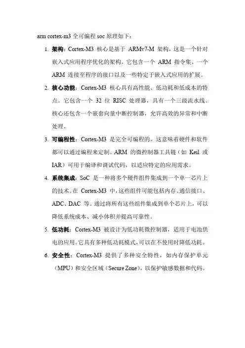
arm cortex-m3全可编程soc原理如下:
1.架构:Cortex-M3 核心是基于ARMv7-M 架构,这是一个针对
嵌入式应用程序优化的架构。
它包含一个ARM 指令集、一个
ARM 连接至程序的接口以及一些特定于嵌入式应用的扩展。
2.核心功能:Cortex-M3 核心具有高性能、低功耗和低成本的特
点。
它包含一个32 位RISC 处理器,具有一个三级流水线。
核心还包含一个嵌套向量中断控制器,允许高效的异常和中断
处理。
3.可编程性:Cortex-M3 是完全可编程的。
这意味着硬件和软件
都可以通过编程来定制。
ARM 的微控制器工具链(如Keil 或
IAR)可用于编译和调试代码,以适应特定的应用需求。
4.系统集成:SoC 是一种将多个硬件组件集成到一个单一芯片上
的技术。
在Cortex-M3 中,这些组件可能包括内存、通信接口、
ADC、DAC 等。
通过将所有这些组件集成到单个芯片上,可以
降低系统成本、减小体积并提高可靠性。
5.低功耗:Cortex-M3 被设计为低功耗微控制器,适用于电池供
电的应用。
它具有多种低功耗模式,可以在不使用时降低功耗。
6.安全性:Cortex-M3 提供了多种安全特性,如内存保护单元
(MPU)和安全区域(Secure Zone),以保护敏感数据和代码。

cortex-m3工作模式工作原理理论说明以及概述1. 引言1.1 概述Cortex-M3是一款基于ARM架构的微控制器处理器,它在嵌入式系统中具有广泛应用的能力。
该处理器以低功耗、高性能和可靠性著称,广泛应用于各种嵌入式系统中,如汽车电子、智能家居、医疗设备等领域。
本文将对Cortex-M3的工作模式和工作原理进行深入探讨,并介绍了相关的理论知识。
1.2 文章结构本文共分为5个部分。
首先,在引言部分简要介绍了Cortex-M3处理器的概述、应用领域和重要性。
其次,在第2部分“Cortex-M3工作模式”中,我们将详细解释什么是Cortex-M3的工作模式,并列举常见的工作模式及其特点,最后还将介绍工作模式之间的切换过程。
第3部分“Cortex-M3工作原理”将对该处理器的架构概述、处理器核心详解以及访存交互机制进行详细说明。
然后,第4部分“Cortex-M3理论说明”将介绍ARM指令集简介、硬件保护和栈管理以及特殊功能寄存器(SFR)的作用和使用方法。
最后,在第5部分“结论”中,我们将对全文进行总结,并提出进一步研究方向的建议。
1.3 目的本文的目的在于全面了解和掌握Cortex-M3处理器的工作模式、工作原理以及相关理论知识。
通过学习本文,读者将能够理解Cortex-M3在嵌入式系统中运行的方式和机制,从而为嵌入式系统设计与开发提供有力支持。
同时,本文还可以为进一步深入研究该领域奠定基础,并为相关技术人员提供参考资料。
2. Cortex-M3工作模式:2.1 工作模式定义:Cortex-M3是一种高性能、低功耗的32位嵌入式处理器核,具备多种工作模式以满足不同应用需求。
工作模式是指处理器在执行任务时所处的状态。
2.2 常见的工作模式:在Cortex-M3中,常见的工作模式包括运行、睡眠和待机。
以下分别介绍这些工作模式:- 运行(Run):在运行模式下,处理器核心处于正常运行状态,可以执行指令,并响应中断请求。
CortexM3技术参考手册CortexM3技术参考手册CortexM3是一种基于ARMv7架构的32位微控制器,由ARM公司开发。
它是一种高效、可编程的微控制器,适用于各种嵌入式应用,如工业控制、汽车电子、智能家居等。
本文将介绍CortexM3的技术参考手册,帮助读者更好地了解该微控制器的功能和使用方法。
一、CortexM3架构CortexM3采用ARMv7架构,支持Thumb和Thumb-2指令集。
它采用32位处理器,具有较高的处理效率和灵活的编程能力。
该微控制器具有以下主要特点:1、处理速度:CortexM3采用ARMv7架构,最高运行速度可达100MHz。
2、存储器:CortexM3内置32KB的Flash存储器,可用于存储程序代码和数据。
此外,它还内置了4KB的SRAM,用于存储临时数据。
3、外设接口:CortexM3具有多种外设接口,包括UART、SPI、I2C、ADC等,可满足各种不同的应用需求。
4、调试接口:CortexM3内置调试接口,方便开发人员对程序进行调试和仿真。
二、CortexM3编程CortexM3的编程主要涉及硬件抽象层(HAL)和驱动程序(Driver)的开发。
其中,HAL提供了一组标准的接口函数,用于访问CortexM3的硬件资源。
驱动程序则是在HAL的基础上开发的,用于实现具体的硬件功能。
三、CortexM3应用实例下面以一个简单的例子来说明如何使用CortexM3实现一个基于UART 的通信接口。
1、硬件连接:将CortexM3的UART接口与另一台设备通过串口连接。
2、软件设置:在CortexM3的HAL中配置UART接口的波特率、数据位、停止位等参数。
3、编写程序:编写一个简单的程序,通过UART接口发送和接收数据。
4、调试与测试:通过调试接口对程序进行调试和测试,确保通信正常。
四、总结本文介绍了CortexM3的技术参考手册,包括其架构、编程和应用实例等。
Cortex-M3分支预测规则一、介绍1. Cortex-M3处理器是一款针对嵌入式系统设计的低功耗高性能处理器,广泛应用于物联网、工业控制等领域。
2. 分支预测是现代处理器优化性能的重要手段之一,Cortex-M3也采用了分支预测技术来提高处理器的执行效率。
3. 在本文中,将详细介绍Cortex-M3分支预测的规则和机制,为开发人员提供最佳的编程指导。
二、分支预测规则1. 无条件分支1.1 无条件分支是指程序中不受条件限制的跳转指令,如跳转到某个标签或函数的入口点。
1.2 Cortex-M3处理器采用静态预测策略来处理无条件分支,即总是假设分支会发生,并预测目标位置区域为分支目标位置区域。
1.3 如果预测正确,则处理器继续执行预测分支的指令;如果预测错误,则处理器需要清空流水线并重新指向正确的位置区域。
2. 有条件分支2.1 有条件分支是根据特定条件进行跳转的指令,比如if-else语句中的条件判断。
2.2 Cortex-M3处理器采用动态预测策略来处理有条件分支,即根据历史执行记录和分支指令的条件来预测分支结果。
2.3 如果预测正确,则处理器继续执行预测分支的指令;如果预测错误,则需要清空流水线并重新指向正确的位置区域。
2.4 另外,Cortex-M3处理器还提供了分支延迟槽的功能,即在分支指令后的一两条指令会被预先执行,以尽量减少分支延迟带来的性能损失。
3. 循环分支3.1 循环分支是一种特殊的有条件分支,通常在循环结构中使用,如for、while等。
3.2 Cortex-M3处理器采用静态预测策略来处理循环分支,即总是假设分支会发生,并预测目标位置区域为循环体的入口位置区域。
3.3 同样地,如果预测正确,则处理器继续执行预测分支的指令;如果预测错误,则需要清空流水线并重新指向正确的位置区域。
4. 分支预测规则总结4.1 无条件分支采用静态预测策略,总是预测分支会发生。
4.2 有条件分支采用动态预测策略,根据历史执行记录和分支条件来预测分支结果。
Cortex—M3学习笔记------Keil+LM3S开发环境的构建Written by PingfKeil RVMDK的安装我就不多说了,我用的是3.23版的.破解顺带提一下.Keil License的导入还是很方便的,两张图足够说明了.下面说一下LM3S的驱动库在说之前,简单说一下Keil的目录/uv3 是开发环境的目录,无论安装哪个版本的Keil都会生成该目录,如果安装了多个版本的Keil,建议安装在同一目录,仍然只会生成一个uv3子目录,但其中的配置文件中的内容会有所改动./ARM安装Keil RVMDK之类for ARM的版本会生成子目录,里面放到自然是与ARM开发相关的东西./*51*具体名字记不清了,安装Keil for 51之类的版本后会生成该目录.Keil RVMDK安装后实际上自带了很多公司的驱动库,当然也包括LuminaryMicro的,下面介绍与编译库相关的几个子目录\Keil\ARM\RV31\LIB\Luminary 这里面放的是Luminary的库文件,比如开发过程中必不可少的那个driverlib就在这里面.\ARM\INC\Luminary 这里面放的是Luminary的库所需要的头文件,实际开发中对头文件的include源自这里.\ARM\Startup\Luminary 这里面就是Luminary器件的启动引导代码了,里面包含了中断向量表之类的东西.实际上前面已经说了,新版的Keil已经自带库了,但若想用最新版的驱动库,还是需要简单的配置一下.Step 1.将\Keil\ARM\RV31\LIB\下的Luminary改为LuminaryBACK,并新建Luminary文件夹,这一步主要是防止错误的发生,先备份一下.Step 2.将库中的所有文件考到新建的Luminary文件夹中[这样做只是为了省事,其中有文件是针对IAR等开发环境的,但本身又不大,省事又方便么]Step 3.按需编译打开\driverlib下的driverlib.Ubv2编译一下,之后在\driverlib\rvmdk下生成driverlib.lib 打开\grlib下的grlib.Uv2编译一下,之后在\grlib\rvmdk下生成grlib.lib打开\usblib下的usblib.Uv2编译一下,之后在\usblib\rvmdk下生成usblib.lib这里要说明的是driverlib对应的是通用库,一般开发就要用到.因此编译它是必须的.grlib对应的是图形库,usblib则对应与usb应用相关的啦.按情况进行啦.在开发过程中需要按需在工程文件中添加上述*.lib文件才能进行库的调用.Step 4.头文件还是找一种省事的方法,搜索库中*.h的文件,全部拷贝到\ARM\INC\Luminary下,重名的覆盖掉就欧科啦.[可能有些不必要,但也没啥可担心的],以后开发时按需include就行了.下面就可以进行开发了.先写到这里,有时间再继续.。
Cortex-M3是一种32位嵌入式处理器核,由ARM公司开发。
在了解Cortex-M3的启动原理之前,需要明确一些基本概念:
复位向量表(Reset Vector Table):复位向量表是存储了一组处理器初始执行的指令的内存区域。
当处理器复位时,它会从复位向量表中获取第一条指令的地址。
复位过程:当Cortex-M3处理器上电或接收到复位信号时,它会执行一系列固定的步骤来进行初始化操作,包括设置栈指针、加载复位向量表等。
下面是Cortex-M3的启动原理的简要说明:
1、上电初始化:当Cortex-M3处理器上电时,会执行一系列的上电初始化操作,包括设置系统时钟、外设初始化等。
2、设置栈指针:处理器需要一个堆栈用于存储函数调用和中断处理。
在启动过程中,需要设置正确的堆栈指针,以确保正确的函数调用和返回。
3、加载复位向量表:处理器会从特定的地址处加载复位向量表。
这个地址通常是存储器的起始地址,可以是内部闪存、外部闪存或其他存储器。
4、处理器复位:复位向量表的第一个条目是复位向量,包含了处理器复位后要执行的第一条指令的地址。
处理器将跳转到该地址并开始执行。
5、初始化操作:在复位向量表中,你可以加载其他初始化代码或配置,如初始化外设、设置中断向量表等。
描述嵌入式操作系统μC/OSII在LM3S系列单片机上实现移植的过程。
介绍操作系统的移植原理和方法,以LM3S8962单片机为例给出部分移植函数的代码,并通过一个实例的应用验证移植的正确性。
引言μC/OSII是一种简单高效、源代码公开的实时嵌入式操作系统,具有良好的扩展性和可移植性,被广泛应用到各种嵌入式处理器上;对于提高产品的质量,减少开发周期和降低成本有着重要的意义。
本文以μC/OSII为移植对象,以ARM CortexM3内核微处理器为移植目标来讨论其移植过程及应用。
1 μC/OSII及ARM CortexM3简介实时操作系统μC/OSII是一个基于优先级的抢占式实时内核,程序可读性强,移植性好,代码固定,可裁剪,非常灵活。
至今,从8位到64位,μC/OSII 已在超过40种不同架构的微处理器上运行。
μC/OSII的主要特点有:是优先级可剥夺的实时多任务操作系统;可处理和调度56个用户任务,任务的优先级可以动态调整;提供任务间通信、同步使用的信号量、邮箱和消息队列;具有良好的可裁剪性,可尽量减小系统的ROM和RAM大小。
ARM是目前嵌入式领域应用最广泛的RISC微处理器结构,它以低成本、低功耗、高性能等优点占据了嵌入式系统应用领域的领先地位。
当前ARM系列的处理器有ARM7、ARM9、ARM9E、ARM10、ARM11等多个产品。
CortexM3内核是 ARM公司于2006年推出的一款高性能处理器内核,是ARM新型 V7指令集结构系列的微控制器版本,可用于企业应用、汽车系统、家庭网络和无线技术等领域。
其主要特点是:① 功耗低;② 内核的门数少,具有优异的性价比;③ 中断延时短;④ 调试成本低;⑤ 具有嵌套向量中断控制器(NVIC),与处理器内核紧密结合实现低延迟的中断处理;⑥ 具有可裁减的存储器保护单元(MPU),用于对存储器进行保护。
2 移植μC/OSIILuminary Micro公司的LM3S系列微控制器包含运行在 50 MHz频率下的ARM CortexM3MCU内核、嵌入式Flash和SRAM、1个低压降的稳压器、集成的掉电复位和上电复位功能、模拟比较器、10位ADC、SSI、GPIO、看门狗和通用定时器、UART、I2C、运动控制PWM以及正交编码器(quadratureencoder)输入,非常适合楼宇和家庭自动化、工厂自动化和控制、工控电源设备、步进电机、有刷和无刷DC马达、AC感应电动机等方面的应用。
SmartFusion2 ARM Cortex-M3 Lab GuideMicrosemi SoC Products Group, San Jose, CA 95134© 2013 Microsemi Corporation. All rights reserved.Printed in the United States of AmericaRelease: April 2013Microsemi makes no warranties with respect to this documentation and disclaims any implied warranties of merchantability or fitness for a particular purpose. Information in this document is subject to change without notice. Microsemi assumes no responsibility for any errors that may appear in this document.This document contains confidential proprietary information that is not to be disclosed to any unauthorized person without prior written consent of Microsemi Corporation.TrademarksMicrosemi, Microsemi Fusion, IGLOO, Libero, ProASIC, SmartFusion, SmartFusion2 and the associated logos are trademarks or registered trademarks of Microsemi Corporation. All other trademarks and service marks are the property of their respective owners.Introduction (4)Components of SmartFusion2 Device Used (4)Tutorial Requirements (5)Extracting the source files (5)Step 1 – Download Firmware Drivers (6)Step 2 – Creating a Libero SoC Project and configuring the SmartFusion2 MSS (7)Launching Libero SoC (7)Opening SmartFusion2_Simple_MSS_MSS_0 in SmartDesign (10)Step 3 – Importing a Physical Constraint file (25)Step 4 – Synthesis and Layout (27)Step 5 – Programming (32)Step 6 – Running the GPIO Application (35)Checking Project Settings and performing a build (38)Debugging with SoftConsole (39)Running the GPIO_interrupt Application (42)Step 7 - Running the polled_uart application (46)Configuring a terminal emulator program (47)Launching the debugger and running the application (49)Answers to Questions (50)List of Figures (51)This tutorial demonstrates how to implement a basic SmartFusion2 microcontroller subsystem (MSS) configuration that includes the GPIO block and MMUART_0 using the SmartFusion2 MSS configurator.The SmartFusion2 GPIO[8] will be configured as an input and GPIO[1:0] will be configured as outputs. The outputs will drive LEDs on the SmartFusion2 Starter kit; GPIO[8] will be connected to one of the switches on the Starter kit board.After completing this tutorial you will be familiar with the following:∙Creating a Libero SoC project∙Configuring the SmartFusion2 MSS and generating the design∙ Generating sample firmware projects from the Firmware catalog∙Synthesizing the SmartFusion2 design with Synplify Pro AE∙Importing a PDC constraint file to pin assignments and running layout on the design∙Generating a programming file and programming the SmartFusion2 device on the Starter Kit board∙Using SoftConsole to download Cortex-M3 applications to the SmartFusion2 Starter Kit board and debug the applicationsFigure 1 - SmartFusion2 Block DiagramComponents of SmartFusion2 Device UsedThis tutorial uses the SmartFusion2 Cortex-M3, the GPIO block and MMUART_0.Tutorial RequirementsSoftware Requirements∙Microsemi Libero SoC v11.0∙ModelSim 10.1c∙Synplify Pro ME G-2012.09MSP1∙FlashPro v11.0∙SoftConsole v3.4∙HyperTerminal or similar software, normally under Start > Programs > Accessories > Communications > HyperTerminal.Note: HyperTerminal is no longer standard on newer windows installations. For alternatives to HyperTerminal, see /windows-7/alternatives-to-hyperterminal-in-windows-7/∙USB Drivers for the FT232R USB to UART IC:/documents/CDM_2.08.24_WHQL_Certified.zipSmartFusion2 MSS Component versionsThe table below lists the version of the SmartFusion2 MSS which must be used.Hardware RequirementsThis tutorial requires the following hardware for verifying the design:∙SmartFusion2 Starter Kit∙FlashPro4 Programmer∙ 2 USB 2.0 A to mini-B cablesExtracting the source filesExtract SF2_Cortex-M3_tutorial.zip to extract the required lab files to the C:\Actelprj folder on the HDD of your PC. Confirm that a folder named SF2_Cortex-M3_tutorial containing a sub-folder named Source_files was extracted.Step 1 – Download Firmware DriversIn order to use the Firmware drivers and sample projects for SmartFusion2 it is necessary to download them from the online Repositories into the IP vault on your machine.1.Open the Microsemi SoC Firmware catalog (Start > Programs > Microsemi Libero SoC v11.0 > Firmware Catalogv11.0 > Firmware Catalog.2.Look for the message New cores are available for download at the bottom of the Firmware Catalog.Figure 2 - New cores message in the Firmware catalog3.Click on Download them now to download all the most recent drivers for peripherals including Sample code andCMSIS compliant HAL etc. The resulting window should look like the figure below.Figure 3 – Firmware Catalog fully Populated4.Close the Firmware Catalog (File > Exit).Step 2 – Creating a Libero SoC Project and configuring the SmartFusion2 MSSIn this step you will create a Libero SoC v11.0_Beta project and configure the SmartFusion2 MSS.Launching Libero SoC1.Click Start > Programs > Microsemi Libero SoC v11.0 > Libero SoC v11.0, or click the shortcut on your desktop. TheLibero SoC Project Manager will open.Figure 4 - Libero SoC v11.0 Project Manager2.Create a new project by selecting New on the Start Page tab (circled in the figure above), or by clicking Project >New Project from the Libero SoC menu. The New Project dialog box will open as shown in the next figure.Figure 5 - Libero SoC v11.0 New Project dialog box3.Click the Edit Tool Profiles button to open the Tool Profiles dialog box (circled in the figure above). Verify that thefollowing tool profiles exist:∙Software IDE: SoftConsole v3.4 contained in <Libero_v11.0_installation>\SoftConsole\Eclipse\exlipse.exe ∙Synthesis: Synplify Pro ME G-2012.09MSP1 contained in<Libero_v11.0_installation>\ Synopsys\synplify_G201209MSP1\binsynplify_pro.exe ∙Simulation: ModelSim AE v10.1c contained in< Libero_v11.0_installation>\Model\win32acoem\modelsim.exe∙Programming: FlashPro v11.0 contained in<Libero_v11.0_installation>\designer\bin\flashpro.exe4.Click OK to close the Tool Profiles dialog box.5.Enter the information shown below in the New Project dialog box:∙Project Name: SmartFusion2_Simple_MSS∙Project Location: C:/Actelprj/SF2_Cortex-M3_tutorial∙Preferred HDL type: Select either VHDL or Verilog based on your HDL preferences∙Family: SmartFusion2∙Die: M2S050T_ES∙Package: 896 FBGA∙Speed: STD∙Core Voltage(V): 1.2∙Ramp Rate: 100ms Minimum∙Operating conditions: COM∙Use Design Tool: checked∙Core: click on SmartFusion2 Microcontroller Subsystem (MSS) 1.0.100 to use the MSS configurator6.If the System Builder or SmartFusion2 Microcontroller subsystem text is in Italics the core is not in your IP vault.Right click on the name of the core and select Download Core.Figure 6 - Libero SoC New Project parameters7.Click OK to close the New project dialog box.Opening SmartFusion2_Simple_MSS_MSS_0 in SmartDesign8.The SmartDesign canvas will open with the SmartFusion2_Simple_MSS_ MSS_0 component visible.Figure 7 – SmartFusion2 MSS in SmartDesign canvas9.Double-click SmartFusion2_Simple_MSS_MSS_0 to open the SmartFusion2 MSS configurator. The MSS configuratorwill appear as shown in the figure below.Figure 8 - SmartFusion2 MSS configuratorMSS peripherals that can be disabled have a small wrench symbol and check box in the lower right corner. To disable a peripheral, select the peripheral, right-click, and select Disable, or click on the checkbox. The peripheral turns grey to indicate a peripheral has been disabled. Disabled peripherals can be enabled by repeating the procedure.10.Disable all of the peripherals that have a checkbox except MMUART_0. Enable the GPIO peripheral.Tip: click View > Maximize Work Area or the Maximize/Restore Work Area button () on the toolbar to expand the working area while using the SmartFusion2 MSS configurator to configure the MSS peripherals.Next configure the GPIO block. For this design we will configure GPIO[1:0] as outputs and GPIO[8] as an input.GPIO[1:0] will be connected to LEDs on the SmartFusion2 starter kit; GPIO[8] will be connected to a switch on the SmartFusion2 starter kit, the GPIOs are brought out to the fabric to match the connections on the SmartFusion2 starter kit board.11.Configure the MSS GPIO block by double-clicking the GPIO in the MSS configurator. Configure the GPIOs as shownbelow.∙Set/Reset Definition: accept default settings∙Configure GPIO[1:0] and GPIO_[8] per the table below:Figure 9 - SmartFusion2 GPIO Configuration 12.Click OK to close the GPIO configurator.13.Double-click the MSS_CCC box in the SmartFusion2 MSS configurator. Enter the following in the CCC configurator:∙CLK_BASE: 100 MHz∙Monitor FPGA Fabric PLL Lock: checked∙M3_CLK: 100 MHz∙APB_0_CLK: M3_CLK / 4 (25 MHz)∙ APB_1_CLK: M3_CLK / 4 (25 MHz)The APB bus clock rate of 25 MHz was selected to match the rates used in the sample firmware projects that will be generated later.Figure 10 - SmartFusion2 MSS CCC configurator14.Click OK to close the CCC configurator.15.After configuring the GPIO block the MSS configurator should appear as shown in the figure below.Figure 11 - SmartFusion2 MSS configurator after configuring GPIOs and Reset16.Save the SmartFusion2_Simple_MSS_MSS component (File > Save SmartFusion2_Simple_MSS_MSS).17.Close the SmartFusion2 MSS configurator (File > Close SmartFusion2_Simple_MSS_MSS).18.If necessary, restore the work area (View > Restore Work Area).19.Select the SmartFusion2_Simple_MSS tab. The SmartFusion2 component (SmartFusion2_Simple_MSS_MSS_0) willbe visible in the SmartDesign canvas. The warning symbol () indicates that the SmartFusion2 component has changed. Right click and select Update Instance(s) with Latest Component. The SmartDesign canvas will resemble the figure below.Figure 12 - SmartDesign canvas with SmartFusion2 MSS componentNext you will add the SmartFusion2 Chip Oscillator and fabric CCC components to the SmartDesign canvas and connect them SmartFusion2 MSS component.20.Expand the Clock & Management category in the Libero SoC IP Catalog.Figure 13 - Libero SoC IP Catalog21.Drag an instance of Chip Oscillators v1.0.100 onto the SmartDesign canvas. If the component appears shadowed inthe Vault, right-click the name and select Download.22.Drag an instance of Clock Conditioning Circuitry (CCC) v2.0.100 onto the SmartDesign canvas. The canvas will appearas shown in the figure below.Figure 14 - SmartDesign canvas after adding OSC and CCC components23.Double-click the OSC_0 component in the SmartDesign canvas to open the SmartFusion2 Chip Oscillatorsconfigurator.24.For this design we will use the On-chip 25/50 MHz RC Oscillator. Configure the Oscillator as follows:∙On Chip 25/50 MHz RC Oscillator: checked∙Drives Fabric (CCCs): checked∙Drives Fabric Logic: un-checkedFigure 15 - On-chip RC oscillator configuration25.Click OK to close the Chip Oscillators Configurator.26.Double-click the FCCC_0 component in the SmartDesign canvas to open the SmartFusion2 Fabric CCC configurator.27.Select the Basic tab in the FAB CCC configurator. Enter the following then click OK:∙Reference clock: Select 25/50 MHz Oscillator from the pull-down menu∙PLL Analog Supply voltage: 3.3V∙ GL0: checked; Frequency = 100 MHzFigure 16 - selecting the FAB CCC reference clockThe PLL Analog Supply voltage can be either 2.5V or 3.3V. The voltage setting in the configurator must match the PLL Analog Supply voltage on the board to ensure the PLL works correctly. The PLL Analog Supply voltage is tied to 3.3V on the SmartFusion2 Starter kit, so the setting must be changed in the FAB CCC configurator above.28.Click OK to close the FAB CCC configurator. The SmartDesign canvas will appear as shown in the figure below.Figure 17 - SmartDesign canvas after configuring the On Chip Oscillatorse the SmartDesign auto connect feature to connect the OSC_0 and CCC_0 blocks by right-clicking in the canvasand selecting Auto Connect.Figure 18 - Auto Connecting the Chip Oscillators and Fabric CCCNext you will make connections using the QuickConnect feature in SmartDesign.30.Click SmartDesign > QuickConnect or right click in the SmartDesign canvas and select QuickConnect. TheQuickConnect dialog box will open.Figure 19 - SmartDesign QuickConnect dialog box31.Connect the FCCC_0:GL0 port to the SmartFusion2_Simple_MSS_MSS_0:MCCC_CLK_BASE port by clicking onCCC_0:GL0 in the left-hand side of the dialog box, clicking MCCC_CLK_BASE underSmartFusion2_Simple_MSS_MSS_0 in the right-hand side of the dialog box, then right-clicking and selecting Connect. The color of the pins will change to green to indicate they are connected.Figure 20 - Using QuickConnect to connect the CCC output to the SmartFusion2 MSS CLK_BASE port32.Repeat the previous step to connect the FCCC_0:LOCK port to theSmartFusion2_Simple_MSS_MSS_0:MCC_CLK_BASE_PLL_LOCK port.33.Promote the SmartFusion2_Simple_MSS_MSS_0:GPIO_0_M2F pin to the top level by clicking in the Connection boxnext to the pin name in the QuickConnect dialog box, then right-clicking and selecting Promote to Top Level.Figure 21 - Using QuickConnect to promote GPIO_0_M2F to the top level34.Repeat the previous step to promote the following SmartFusion2_Simple_MSS_MSS_0:GPIO_0 ports to the toplevel:∙GPIO_1_M2F∙GPIO_8_F2M35.After promoting the pins to the top level, the connected pins will be highlighted green and displayed in the right-hand side of the QuickConnect dialog box as shown in the figure below.Figure 22 - QuickConnect dialog box after making connections and promoting pins to the top level36.Click Close to close the QuickConnect dialog box.37.The canvas will appear as shown in the figure below. If necessary, right click in the canvas and select AutoArrangeInstances or Route All Nets to improve the appearance of the canvas.Figure 23 - SmartDesign canvas after connecting the RC oscillator to the SmartFusion2 MSS38.Save the design (File > Save SmartFusion2_Simple_MSS).39.Open the Libero SoC project settings (Project > Project Settings).40.Select Device I/O Settings in the Project Settings dialog box. Select LVCMOS 3.3V from the pull-down list in theDefault I/O Technology field.Figure 24 - Selecting the default I/O attribute41.Click Save. Select Yes in the Warning dialog box that appears.42.Close to close the Project Settings dialog box.43.Open the SmartDesign DESIGN FIRMWARE tab (Design > Configure Firmware).44.Confirm that none of the drivers appear in italics. If any drivers appear in italics, click the Download All Firmwarebutton (circled in the figure below).45.Confirm that the check box in the Generate column is checked for all of the drivers as shown in the figure below.Figure 25 - SmartDesign Design Firmware tab46.Create the GPIO Simple Blink sample project by selecting SmartFusion2_MSS_GPIO_Driver_0 on the DESIGNFIRMWARE tab, then right clicking and selecting Generate Sample Project > Cortex-M3 > SoftConsole > Simple Blink.Figure 26 - Generating the Simple Blink sample project47.Confirm the following settings in the Generate Sample Options dialog box then click OK:∙Samples folder: C:\Actelprj\SF2_Cortex-M3_tutorial\SmartFusion2_Simple_MSS ∙Show generation report: checkedFigure 27 – Simple Blink sample project options48.The Report dialog box will list all the files generated and the location.Figure 28 - GPIO Simple Blink project files49.Click Close to close the Report window.50.Create the Polled UART sample project by selecting SmartFusion2_MSS_MMUART_Driver_0 on the DESIGNFIRMWARE tab, then right clicking and selecting Generate Sample Project > Cortex-M3 > SoftConsole > Polled UART.51.Confirm the following settings in the Generate Sample Options dialog box then click OK:∙Samples folder: C:\Actelprj\SF2_Cortex-M3_tutorial\SmartFusion2_Simple_MSS∙Show generation report: checkedFigure 29 – Polled UART sample project options52.The Report dialog box will list all the files generated and the location.Figure 30 - Simple Blink project files53.Click Close to close the Report window.54.Close the DESIGN FIRMWARE tab (File > Close DESIGN FIRMWARE). Select Yes if prompted about saving changes toDESIGN_FIRMWARE.55.The sample projects will be visible on the Libero SoC Files tab. If the projects are not visible, select View > RefreshDesign Hierarchy from the Libero SoC menu.Figure 31 - Sample projects on Libero SoC Files tab56.Click the SmartFusion2_Simple_MSS tab in the SmartDesign canvas area if the design is not visible. Generate theSmartFusion2_Simple_MSS component by clicking SmartDesign > Generate Component or by clicking the GenerateComponent icon on the SmartDesign toolbar ().57.The messages “SoftConsole workspace was successfully generated” and “SmartFusion2_Simple_MSS' wassuccessfully generated” will appear in the Libero SoC log window if the design was generated without any errors. In addition, a green check mark will appear in under Create Design in the Libero SoC Design Flow window indicating the design was created without any errors.Figure 32 - Successful creation of SmartDesign component58.Close the design (File > Close SmartFusion2_Simple_MSS).59.Open the Reports tab by clicking Design > Reports or by clicking the Reports icon () in the Libero SoC toolbar.The Reports tab will be visible in the SmartDesign working area.60.Open the SmartFusion2_Simple_MSS data sheet by clicking SmartFusion2_Simple_MSS_DataSheet.xml in thereports tab.Figure 33 - Opening the SmartFusion2_Simple_MSS data sheet61.Scroll in the SmartFusion2_Simple_MSS data sheet and become familiar with the Generated Files, Firmware andMemory Map sections (click on the hyperlink at the top of the data sheet to move to the section of interest).Answer the following questions:What is the address of the GPIO? ___________________________What is the address of MMUART_0? ___________________________Step 3 – Importing a Physical Constraint fileIn this step you will use a Physical Constraint file to make pin assignments and I/O attribute assignments for layout. There are multiple ways to make I/O Assignments. For this lab you will import a Physical Design Constraint (PDC) file that has been provided to make I/O attribute and pin assignments.1.Expand Create Constraints in the Design Flow window. Select I/O Constraints then right-click and select ImportFiles.. .Figure 34 - Importing the PDC constraint file2.Enter the following in the Import Files dialog box then click Open:Look in: C:\Actelprj\SF2_Cortex-M3_tutorial\Source_files∙Files of type: I/O Constraint Files (*.pdc)∙File name: SmartFusion2_Simple_MSS_IO.pdc3.Select No in the Information dialog box.Figure 35 - Information dialog box after importing the PDC constraint file4.The file will be visible on the Libero SoC Files tab under constraint > io.Figure 36 - PDC constraint file in the Libero SoC project5.Double-click the PDC file name on the Files tab to open the file in the Libero SoC editor. Scroll in the file to becomefamiliar with the syntax.The constraint set_iobank sets the input voltage of the bank to determine the allowable I/O standards; theconstraint set_io sets the pin number and I/O specific attributes. The # symbol is a comment.6.Close the editor (File > Close SmartFusion2_Simple_MSS_IO.pdc).For more information regarding pin assignments for the Starter Kit board, see the Starter Kit schematic (som-bsb-ext-1a-schem.pdf) which is available from the SmartFusion2 Starter Kit web page.A description of the Designer PDC constraints is available in the Libero Help (Help > Help Topics > Implement Design> Constrain Place and Route > Assigning Design Constraints > Design Constraints Guide > Reference > Constraints by File Format > PDC Command Reference).Step 4 – Synthesis and LayoutIn this step you will use the push-button flow to synthesize the design with Synplify Pro, run layout and generate the programming file.1.Expand Create Constraints > I/O Constraints in the Libero SoC Design Flow window. Right-clickSmartFusion2_Simple_MSS_IO.pdc under Constraints then right-click and select Use for Compile. A green check mark will appear next to the constraint file indicating that the file will be used.Figure 37 - Selecting the PDC constraint file in the Design Flow window2.Expand Implement Design on the Design Flow tab. Right-click Compile and select Configure Options.Figure 38 - Configuring Compile Options3.The Configuring dialog box will open. Un-check “Abort Compile if errors are found in the physical designconstraints” then click OK.Figure 39 - Configuring the Compile Options4.Disable Timing Driven Layout by right-clicking Place and Route in the Libero Designer Flow window and selectingConfigure Options.Figure 40 - Configuring Designer layout options5.The Configuring dialog box will open. Un-check Timing-driven and then click OK.Figure 41 - Disabling timing driven layout6.Click the Generate Programming Data icon in the Design Flow window (circled in the figure below) or select Design >Generate Fabric Programming Data to synthesize the design, run layout using the I/O constraints that were created and generate the programming file.Figure 42 - Generate Programming Data icon7.The design implementation tools will run in batch mode. Click Yes in the warning dialog box to generate the fabricprogramming data without having all the IOs assigned.Figure 43 - Warning dialog boxSuccessful completion of a design step will be indicated by a green check mark next to the Implement Design in the Design Flow window.Figure 44 – Successful completion of design implementation8.The Reports tab will display reports for the tools used to implement the design.Figure 45 - Reports tab after implementing the design9.The output files from Synplify Pro and Designer will be visible on the Libero SoC Files tab.Figure 46 - Synthesis and Designer files on Libero SoC Files tabStep 5 – ProgrammingIn this step you will run FlashPro in batch mode to program the SmartFusion2 M2S050T on the SmartFusion2 Starter Kit board.1.Prior to programming (and powering up) the SmartFusion2 Starter Kit board, confirm that the jumpers arepositioned as show in the table below.2.Connect the mini-USB Y-cable into the mini-USB connector labeled USB Power & USB UART I/F (P1) connector onSOM-BSB-EXT board (see figure above). As soon as the connection to the PC has been made, the on-board LED DS2 will illuminate, indicating that the board has power.A single USB connection provides a 500 mA power to the SF2-STARTER-KIT-ES, which is sufficient for basicfunctionality. Note however that some advanced operations, such as WiFi connectivity using the USB WiFi module, may require more than 500 mA for reliable operation. Use the second link of the mini-USB Y-cable to connect to the PC for such configurations.If prompted, install the FT232R drivers. The drivers can be downloaded from/documents/CDM_2.08.24_WHQL_Certified.zip3.Plug the FlashPro4 ribbon cable into 10 pin connector (P5) on the Starter Kit board.4.Connect the mini USB cable between the FlashPro4 and the USB port of your PC.5.Install the FlashPro4 drivers if prompted. The drivers are located in the <FlashPro Installation Directory>\Driversfolder.6.Expand Program Design in the Design Flow window. Right-click Program Device and select Run to beginprogramming.Figure 48 - Launching Programming software from Design Flow window7.FlashPro will run in batch mode and program the device. Programming messages will be visible in the Libero SoC logwindow (programmer number will differ).Note: Do not interrupt the programming sequence; it may damage the device or the -programmer.8.The following message should be visible in the Libero SoC Reports view under Program Device when the device isprogrammed successfully (programmer number will differ):programmer '81316' : device 'M2S050T_ES' : Executing action PROGRAM PASSED.9.If you are using the ES silicon a dialog box will remind you to power-cycle the board when programming is complete.Cycle the power on the board by disconnecting and re-connecting the USB cable the mini-USB connector labeled USB Power & USB UART I/F (P1).Figure 49 - Reminder to power cycle the board10.Click OK to close the Program Device dialog box.Figure 50 - Programming messages in Libero SoC Reports window11.A green check mark will appear next to Program Design and Program Device in the Design Flow window to indicateprogramming completed successfully.Figure 51 - Design Flow window after programmingStep 6 – Running the GPIO ApplicationIn this step you will launch SoftConsole v3.4 and run the Simple Blink application.1.Expand Develop Firmware in the Design Flow window. Double-click Write Application code to launch SoftConsole.Figure 52 - Write Application code in Design Flow window2.SoftConsole will open with two projects (SmartFusion2_Simple_MSS_MSS_CM3_app andSmartFusion2_Simple_MSS_MSS_CM3_hw_platform) visible in the Project Explorer view.The SmartFusion2_Simple_MSS_MSS_CM3_app project is the starting point for user applications; the file main.c is a template file that you can use to create your firmware application.The SmartFusion2_Simple_MSS_MSS_CM3_hw_platform project contains the firmware drivers that were created by SmartDesign and the platform header file (SmartFusion2_Simple_MSS _hw_platform.h) which contains theaddresses of any fabric peripherals.3.Expand the folders to become familiar with the contents of each project (Figure 53).Figure 53 – SoftConsole 3.44.Import the main.c file from GPIO simple_blink sample project created earlier by clicking File > Import from theSoftConsole menu. The Import dialog box will open.5.Expand the General category in the Import dialog box and select File System and then click Next. The Import dialogbox will open.6.Enter the following in the Import Projects dialog box:∙From directory: C:\Actelprj\SF2_Cortex-M3_tutorial\SmartFusion2_Simple_MSS\SF2_GNU_GPIO_simple_blink ∙Select main.c∙Into Folder: SmartFusion2_Simple_MSS_MSS_CM3_appFigure 54 - Importing the main.c file from the simple_blink project7.Click Finish. Select Yes when prompted about overwriting main.c in SmartFusion2_Simple_MSS_MSS_CM3_app.The file will be visible in the SoftConsole Project Explorer window as shown below.Figure 55 - SoftConsole projects8.Double click main.c in the Project Explorer window to open the file in the SoftConsole C/C++ editor. Scroll throughthe file to become familiar with it. The comments at the top of the file describe what the program does.Checking Project Settings and performing a build9.Select the project name (SmartFusion2_Simple_MSS_MSS_CM3_app) in the SoftConsole Project Explorer View.10.Select Project > Properties.The project properties dialog box will open.11.Expand C/C++ Build in the properties dialog box and select Settings. Confirm that the Debug configuration isselected.Figure 56 - SoftConsole project settings12.Select Miscellaneous under GNU C Linker. Confirm that the Linker flags field contains-T../../SmartFusion2_Simple_MSS_MSS_CM3_hw_platform/CMSIS/startup_gcc/debug-in-microsemi-smartfusion2-esram.ldThis command uses the linker script that builds an executable that will run from the SmartFusion2 embedded SRAM.。