PartE1_SDIO_Simplified_Specification_Ver3.00
- 格式:pdf
- 大小:391.05 KB
- 文档页数:90
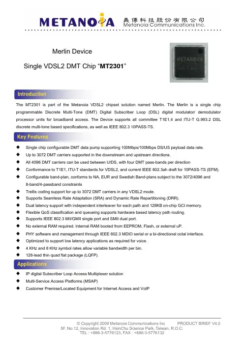
Merlin DeviceSingle VDSL2 DMT Chip “MT2301”The MT2301 is part of the Metanoia VDSL2 chipset solution named Merlin. The Merlin is a single chip programmable Discrete Multi-Tone (DMT) Digital Subscriber Loop (DSL) digital modulator/ demodulator processor units for broadband access. The Device supports all committee T1E1.4 and ITU-T G.993.2 DSL discrete multi-tone based specifications, as well as IEEE 802.3 10PASS-TS.Single chip configurable DMT data pump supporting 100Mbps/100Mbps DS/US payload data rate. Up to 3072 DMT carriers supported in the downstream and upstream directions.All 4096 DMT carriers can be used between U/DS, with four DMT pass-bands per directionConformance to T1E1, ITU-T standards for VDSL2, and current IEEE 802.3ah draft for 10PASS-TS (EFM). Configurable band-plan, conforms to NA, EUR and Swedish Band-plans subject to the 3072/4096 and 8-band/4-passband constraintsTrellis coding support for up to 3072 DMT carriers in any VDSL2 mode.Supports Seamless Rate Adaptation (SRA) and Dynamic Rate Repartitioning (DRR).Dual latency support with independent interleaver for each path and 128KB on-chip GCI memory. Flexible QoS classification and queueing supports hardware based latency path routing. Supports IEEE 802.3 MII/GMII single port and SMII dual port.No external RAM required. Internal RAM booted from EEPROM, Flash, or external uP.PHY software and management through IEEE 802.3 MDIO serial or a bi-directional octal interface. Optimized to support low latency applications as required for voice. 4 KHz and 8 KHz symbol rates allow variable bandwidth per bin.128-lead thin quad flat package (LQFP).Introduction Key Features Applications IP digital Subscriber Loop Access Multiplexer solution Multi-Service Access Platforms (MSAP)Customer Premise/Located Equipment for Internet Access and VoIPMerlinVDSL ChipMT 2301MTU/MDU IP DSLAM/ORD。
Technical Committee SD Card AssociationRevision HistoryDate Version Changes compared to previous issue April 3, 2006 1.10 Simplified Version Initial ReleaseFebruary 8, 2007 2.00 (1) Added method to change bus speed (Normal Speed up to 25MHzand High Speed up to 50 MHz)(2) Operational Voltage Requirement is extended to 2.7-3.6V(3) Combine sections 12 (Physical Properties) and 13 (MechanicalExtensions) and add miniSDIO to the new section 13 (PhysicalProperties)(4) Add Embedded SDIO ATA Standard Function Interface Code(5) Reference of Physical Ver2.00 supports SDHC combo card.(6) Some typos in Ver1.10 are fixed.Release of SD Simplified SpecificationThe following conditions apply to the release of the SD simplified specification ("Simplified Specification") by the SD Card Association. The Simplified Specification is a subset of the complete SD Specification which is owned by the SD Card Association.Publisher:SD Association2400 Camino Ramon, Suite 375San Ramon, CA 94583 USATelephone: +1 (925) 275-6615Fax: +1 (925) 886-4870E-mail: office@Copyright Holder:The SD Card AssociationNotes:This Simplified Specification is provided on a non-confidential basis subject to the disclaimers below. Any implementation of the Simplified Specification may require a license from the SD Card Association or other third parties.Disclaimers:The information contained in the Simplified Specification is presented only as a standard specification for SD Cards and SD Host/Ancillary products and is provided "AS-IS" without any representations or warranties of any kind. No responsibility is assumed by the SD Card Association for any damages, any infringements of patents or other right of the SD Card Association or any third parties, which may result from its use. No license is granted by implication, estoppel or otherwise under any patent or other rights of the SD Card Association or any third party. Nothing herein shall be construed as an obligation by the SD Card Association to disclose or distribute any technical information, know-how or other confidential information to any third party.Conventions Used in This DocumentNaming ConventionsSome terms are capitalized to distinguish their definition from their common English meaning. Words not capitalized have their common English meaning.Numbers and Number BasesHexadecimal numbers are written with a lower case “h” suffix, e.g., FFFFh and 80h.Binary numbers are written with a lower case “b” suffix (e.g., 10b).Binary numbers larger than four digits are written with a space dividing each group of four digits, as in 1000 0101 0010b.All other numbers are decimal.Key WordsMay: Indicates flexibility of choice with no implied recommendation or requirement.Shall: Indicates a mandatory requirement. Designers shall implement such mandatory requirements to ensure interchangeability and to claim conformance with the specification.Should: Indicates a strong recommendation but not a mandatory requirement. Designers should give strong consideration to such recommendations, but there is still a choice in implementation.Application NotesSome sections of this document provide guidance to the host implementers as follows:Application Note:This is an example of an application note.Table of Contents1.General Description (1)1.1SDIO Features (1)1.2Primary Reference Document (1)1.3Standard SDIO Functions (1)2.SDIO Signaling Definition (2)2.1SDIO Card Types (2)2.2SDIO Card modes (2)2.2.1SPI (Card mandatory support) (2)2.2.21-bit SD Data Transfer Mode (Card Mandatory Support) (2)2.2.34-bit SD Data Transfer Mode (Mandatory for High-Speed Cards, Optional for Low-Speed) (2)2.3SDIO Host Modes (2)2.4Signal Pins (3)3.SDIO Card Initialization (4)3.1Differences in I/O card Initialization (4)3.2The IO_SEND_OP_COND Command (CMD5) (10)3.3The IO_SEND_OP_COND Response (R4) (11)3.4Special Initialization considerations for Combo Cards (12)3.4.1Re-initialize both I/O and Memory (12)3.4.2Using a Combo Card as SDIO only or SD Memory only after Combo Initialization (12)3.4.3Acceptable Commands after Initialization (12)3.4.4Recommendations for RCA after Reset (12)3.4.5Enabling CRC in SPI Combo Card (14)4.Differences with SD Memory Specification (15)4.1SDIO Command List (15)4.2Unsupported SD Memory Commands (15)4.3Modified R6 Response (16)4.4Reset for SDIO (16)4.5Bus Width (16)4.6Card Detect Resistor (17)4.7Timings (17)4.8Data Transfer Block Sizes (18)4.9Data Transfer Abort (18)4.9.1Read Abort (18)4.9.2Write Abort (18)4.10Changes to SD Memory Fixed Registers (18)4.10.1OCR Register (19)4.10.2CID Register (19)4.10.3CSD Register (19)4.10.4RCA Register (19)4.10.5DSR Register (19)4.10.6SCR Register (19)4.10.7SD Status (19)4.10.8Card Status Register (19)5.New I/O Read/Write Commands (21)5.1IO_RW_DIRECT Command (CMD52) (21)5.2IO_RW_DIRECT Response (R5) (22)5.2.1CMD52 Response (SD modes) (22)5.2.2R5, IO_RW_DIRECT Response (SPI mode) (23)5.3IO_RW_EXTENDED Command (CMD53) (24)5.3.2Special Timing for CMD53 Multi-Block Read (25)6.SDIO Card Internal Operation (26)6.1Overview (26)6.2Register Access Time (26)6.3Interrupts (26)6.4Suspend/Resume (27)6.5Read Wait (27)6.6CMD52 During Data Transfer (27)6.7SDIO Fixed Internal Map (27)6.8Common I/O Area (CIA) (28)6.9Card Common Control Registers (CCCR) (28)6.10Function Basic Registers (FBR) (35)6.11Card Information Structure (CIS) (37)6.12Multiple Function SDIO Cards (37)6.13Setting Block Size with CMD53 (37)6.14Bus State Diagram (38)7.Embedded I/O Code Storage Area (CSA) (39)7.1CSA Access (39)7.2CSA Data Format (39)8.SDIO Interrupts (40)8.1Interrupt Timing (40)8.1.1SPI and SD 1-bit Mode Interrupts (40)8.1.2SD 4-bit Mode (40)8.1.3Interrupt Period Definition (40)8.1.4Interrupt Period at the Data Block Gap in 4-bit SD Mode (Optional) (40)8.1.5Inhibited Interrupts (Removed Section) (40)8.1.6End of Interrupt Cycles (40)8.1.7Terminated Data Transfer Interrupt Cycle (41)8.1.8Interrupt Clear Timing (41)9.SDIO Suspend/Resume Operation (42)10.SDIO Read Wait Operation (43)11.Power Control (44)11.1Power Control Overview (44)11.2Power Control support for SDIO Cards (44)11.2.1Master Power Control (44)11.2.2Power Selection (45)11.2.3High-Power Tuples (45)11.3Power Control Support for the SDIO Host (45)11.3.1Version 1.10 Host (45)11.3.2Power Control Operation (46)12.High-Speed Mode (47)12.1SDIO High-Speed Mode (47)12.2Switching Bus Speed Mode in a Combo Card (47)13.SDIO Physical Properties (48)13.1SDIO Form Factors (48)13.2Full-Size SDIO (48)13.3miniSDIO (48)14.SDIO Power (48)14.1SDIO Card Initialization Voltages (48)14.2SDIO Power Consumption (48)15.Inrush Current Limiting (50)16.CIS Formats (51)16.2Basic Tuple Format and Tuple Chain Structure (51)16.3Byte Order Within Tuples (51)16.4Tuple Version (52)16.5SDIO Card Metaformat (52)16.6CISTPL_MANFID: Manufacturer Identification String Tuple (53)16.7SDIO Specific Extensions (53)16.7.1CISTPL_FUNCID: Function Identification Tuple (53)16.7.2CISTPL_FUNCE: Function Extension Tuple (54)16.7.3CISTPL_FUNCE Tuple for Function 0 (common) (54)16.7.4CISTPL_FUNCE Tuple for Function 1-7 (55)16.7.5CISTPL_SDIO_STD: Function is a Standard SDIO Function (58)16.7.6CISTPL_SDIO_EXT: Tuple Reserved for SDIO Cards (58)Appendix A (59)A.1 SD and SPI Command List (59)Appendix B (61)B.1 Normative References (61)Appendix C (62)C.1Abbreviations and Terms (62)Appendix D (64)Table 3-1 OCR Values for CMD5 (10)Table 4-1 Unsupported SD Memory Commands (16)Table 4-2 R6 response to CMD3 (16)Table 4-3 SDIO R6 Status Bits (16)Table 4-4 Combo Card 4-bit Control (17)Table 4-5 Card Detect Resistor States (17)Table 4-6 is blanked (17)Table 4-7 SDIO Status Register Structure (20)Table 5-1 Flag data for IO_RW_DIRECT SD Response (23)Table 5-2 IO_RW_ EXTENDED command Op Code Definition (24)Table 5-3 Byte Count Values (25)Table 6-1 Card Common Control Registers (CCCR) (29)Table 6-2 CCCR bit Definitions (34)Table 6-3 Function Basic Information Registers (FBR) (35)Table 6-4 FBR bit and field definitions (36)Table 6-5 Card Information Structure (CIS) and reserved area of CIA (37)Table 11-1 Reference Tuples by Master Power Control and Power Select (45)Table 16-1 Basic Tuple Format (51)Table 16-2 Tuples Supported by SDIO Cards (52)Table 16-3 CISTPL_MANFID: Manufacturer Identification Tuple (53)Table 16-4 CISTPL_FUNCID Tuple (53)Table 16-5 CISTPL_FUNCE Tuple General Structure (54)Table 16-6 TPLFID_FUNCTION Tuple for Function 0 (common) (54)Table 16-7 TPLFID_FUNCTION Field Descriptions for Function 0 (common) (54)Table 16-8 TPLFID_FUNCTION Tuple for Function 1-7 (55)Table 16-9 TPLFID_FUNCTION Field Descriptions for Functions 1-7 (57)Table 16-10 TPLFE_FUNCTION_INFO Definition (57)Table 16-11 TPLFE_CSA_PROPERTY Definition (57)Table 16-12 CISTPL_SDIO_STD: Tuple Reserved for SDIO Cards (58)Table 16-13 CISTPL_SDIO_EXT: Tuple Reserved for SDIO Cards (58)Table A-14 SD Mode Command List (59)Table A-15 SPI Mode Command List (60)Figure 2-1 Signal connection to two 4-bit SDIO cards (3)Figure 3-1 SDIO response to non-I/O aware initialization (4)Figure 3-2 Card initialization flow in SD mode (SDIO aware host) (7)Figure 3-3 Card initialization flow in SPI mode (SDIO aware host) (9)Figure 3-4 IO_SEND_OP_COND Command (CMD5) (10)Figure 3-5 Response R4 in SD mode (11)Figure 3-6 Response R4 in SPI mode (11)Figure 3-7 Modified R1 Response (11)Figure 3-8 Re-Initialization Flow for I/O Controller (13)Figure 3-9 Re-Initialization Flow for Memory controller (13)Figure 5-1 IO_RW_DIRECT Command (21)Figure 5-2 R5 IO_RW_DIRECT Response (SD modes) (22)Figure 5-3 IO_RW_DIRECT Response in SPI Mode (23)Figure 5-4 IO_RW_EXTENDED Command (24)Figure 6-1 SDIO Internal Map (28)Figure 6-2 State Diagram for Bus State Machine (38)Description1. GeneralThe SDIO (SD Input/Output) card is based on and compatible with the SD memory card. This compatibility includes mechanical, electrical, power, signaling and software. The intent of the SDIO card is to provide high-speed data I/O with low power consumption for mobile electronic devices. A primary goal is that an SDIO card inserted into a non-SDIO aware host shall cause no physical damage or disruption of that host or it’s software. In this case, the SDIO card should simply be ignored. Once inserted into an SDIO aware host, the detection of the card proceeds via the normal means described in this specification with some extensions. In this state, the SDIO card is idle and draws a small amount of power (15 mA averaged over 1 second). During the normal initialization and interrogation of the card by the host, the card identifies itself as an SDIO card. The host software then obtains the card information in a tuple (linked list) format and determines if that card’s I/O function(s) are acceptable to activate. This decision is based on such parameters as power requirements or the availability of appropriate software drivers. If the card is acceptable, it is allowed to power up fully and start the I/O function(s) built into it.Features1.1 SDIO•Targeted for portable and stationary applications•Minimal or no modification to SD Physical bus is required•Minimal change to memory driver software•Extended physical form factor available for specialized applications•Plug and play (PnP) support•Multi-function support including multiple I/O and combined I/O and memory•Up to 7 I/O functions plus one memory supported on one card.•Allows card to interrupt host•Operational Voltage range: 2.7-3.6V (Operational Voltage is used for Initialization)• Application Specifications for Standard SDIO Functions.•Multiple Form Factors:• Full-Size SDIO• miniSDIODocument1.2 PrimaryReferenceThis specification is based on and refers extensively to the SDA document:SD Memory Card SpecificationsPart 1 PHYSICAL LAYER SPECIFICATION Version 2.00 May 9, 2006The reader is directed to this document for more information on the basic operation of SD cards. In addition, other documents are referenced in this specification. A complete list can be found in appendix B.1.This specification can apply to any released versions of Physical Layer Specification after Version 2.00.Functions1.3 StandardSDIOAssociated with the base SDIO specification, there are several Application Specifications for Standard SDIO Functions. These common functions such as cameras, Bluetooth cards and GPS receivers have a standard register interface, a common operation method and a standard CIS extension. Implementation of the standard interfaces are optional for any card vendor, but compliance with the standard allows the use of standard drivers and applications which will increase the appeal of these cards to the consumer. Full information on these standard interfaces can be found in the Application Specifications for Standard SDIO Functions maintained by the SDA.2.SDIO Signaling Definition2.1 SDIO Card TypesThis specification defines two types of SDIO cards. The Full-Speed card supports SPI, 1-bit SD and the 4-bit SD transfer modes at the full clock range of 0-25MHz. The Full-Speed SDIO cards have a data transfer rate of over 100 Mb/second (10 MB/Sec). A second version of the SDIO card is the Low-Speed SDIO card. This card requires only the SPI and 1-bit SD transfer modes. 4-bit support is optional. In addition, Low-Speed SDIO cards shall support a full clock range of 0-400 KHz. The intended use of Low-Speed cards is to support low-speed I/O capabilities with a minimum of hardware. The Low-Speed cards support such functions as modems, bar-code scanners, GPS receivers etc. If a card is a ‘Combo card’ (memory plus SDIO) then Full-Speed and 4-bit operation is mandatory for both the memory and SDIO portions of the card.2.2 SDIO Card modesThere are 3 signaling modes defined for SD memory cards that also apply to SDIO Card:2.2.1 SPI (Card mandatory support)The SPI bus topology is defined in section 3.5.2 and the protocol is defined in sections 3.6.2 and 7 of the SD Physical Specification Version 2.00. In this mode pin 8, which is undefined for memory, is used as the interrupt pin. All other pins and signaling protocols are identical to the SD Physical Specification.2.2.2 1-bit SD Data Transfer Mode (Card Mandatory Support)This mode is identical to the 1 data bit (narrow) mode defined for SD Memory in section 3.6.1 of the SD Physical Specification. In this mode, data is transferred on the DAT[0] pin only. In this mode pin 8, which is undefined for memory, is used as the interrupt pin. All other pins and signaling protocols are identical to the SD Memory specification.2.2.3 4-bit SD Data Transfer Mode (Mandatory for High-Speed Cards, Optional for Low-Speed) This mode is identical to the 4 data bit mode (wide) defined for SD Memory in section3.6.1 of the SD Physical Specification. In this mode, data is transferred on all 4 data pins (DAT[3:0]). In this mode the interrupt pin is not available for exclusive use as it is utilized as a data transfer line. Thus, if the interrupt function is required, a special timing is required to provide interrupts. See section 8.1.2 for details of this operation. The 4-bit SD mode provides the highest data transfer possible, up to 100 Mb/sec.2.3 SDIO Host ModesIf a SDIO aware host supports the SD transfer mode, it is recommended that both the 1-bit and 4-bit modes be supported. While a SDIO host that supports only the 4-bit transfer mode is possible, its performance with a Low-Speed SDIO card may be reduced. This is because the only means to transfer data to and from a Low-Speed card would be the single byte per command transfer (using the IO_RW_DIRECT command (CMD52) see 5.1).2.4 SignalPinsThe rest of this chapter is not included in the Simplified Specification.InitializationCard3. SDIO3.1 Differences in I/O card InitializationA requirement for the SDIO specification is that an SDIO card shall not cause non-I/O aware hosts to fail when inserted. In order to prevent operation of I/O functions in non-I/O aware hosts, a change to the SD card identification mode flowchart is needed. A new command (IO_SEND_OP_COND, CMD5) is added to replace the ACMD41 for SDIO initialization by I/O aware hosts (see 3.2).After reset or power-up, all I/O functions on the card are disabled and the I/O portion of the card shall not execute any operation except CMD5 or CMD0 with CS=low. If there is SD memory installed on the card (also called a combo card), that memory shall respond normally to all normal mandatory memory commands.An I/O only card shall not respond to the ACMD41 and thus appear initially as an MMC card (See appendix B.1 for information on the MMC specification). The I/O only card shall also not respond to the CMD1 used to initialize the MMC cards and appear as a non-responsive card. The host then gives up and disables this card. Thus, the non-aware host receives no response from an I/O only card and force it to the inactive state. The operation of an I/O card with a non-I/O aware host is shown in Figure 3-1 Note that the solid lines are the actual paths taken while the dashed lines are not executed.Figure 3-1 SDIO response to non-I/O aware initializationAn SDIO aware host sends CMD5 prior to the CMD55/ACMD41 pair, and thus would receive a valid OCR in the R4 response to CMD5 and continue to initialize the card. Figure 3-2 shows the operation of an SDIO aware host operating in the SD modes and Figure 3-3 shows the same operation for a host that operates in the SPI mode. If the I/O portion of a card has received no CMD5, the I/O section remains inactive and shall not respond to any command except CMD5. A combo card stays in the memory-only mode. If no memory is installed on the card (i.e. an I/O only card in a non-SDIO aware host) the card would not respond to any memory command. This satisfies the condition where a user uses some I/O function on the card such as Ethernet to load a music file to the memory function of that card. The card is then removed and inserted into a non-SDIO aware host. That host would not enable the I/O function (no CMD5) so would appear to the player as a memory-only card. If the host were I/O aware, it would send the CMD5 to the card and the card would respond with R4. The host reads that R4 value and knows the number of available I/O functions and about the existence of any SD memory.After the host has initialized the I/O portion of the card, it then reads the Common Information Area (CIA) of the card (see 6.8). This is done by issuing a read command, starting with the byte at address 0x00, of I/O function 0. The CIA contains the Card Common Control Registers (CCCR) and the Function Basic Registers (FBR). Also included in the CIA are pointers to the card’s common Card Information Structure (CIS) and each individual function’s CIS. The CIS structure is defined in section 16. The CIS includes information on power, function, manufacturer and other things the host needs to determine if the I/O function(s) is appropriate to power-up. If the host determines that the card should be activated, a register in the CCCR area enables the card and each individual function. At this time, all functions of the I/O card are fully available. In addition, the host can control the power consumption and enable/disable interrupts on a function-by-function basis. This access to I/O does not interfere with memory access to the card if present.Combo Cards can accept CMD15 with RCA=0000, as described in, but there is an exception for SD memory only cards. Memory only cards require a non-zero RCA before the host may issue CMD15. Thus, CMD15 shall be issued after CMD3 in the Standby state. In the case of ACMD41, it shall accept RCA=0x0000.As shown in Figure 3-2 and Figure 3-3, an SDIO aware host shall send CMD5 arg=0 as part of the initialization sequence after either Power On or a CMD 52 with write to I/O Reset. Sending CMD5 arg=0 that has not been preceded by one of these two reset conditions shall not result in either the host or card entering the initialization sequence.VariablesNF: Number of I/O Functions (CMD5 Response) MP: MemoryPresentFlag (CMD5 Response) IORDY: I/O Power-up Status (C bit in the CMD5 response) MRDY: Memory Power-up Status (OCR Bit31)HCS: Host Capacity Support (ACMD41 Argument) CCS: Card Capacity Status (ACMD41 Response) FlagsIO: I/O Functions Initialized FlagMEM: Memory Initialized FlagF8: CMD8FlagVariablesNF: Number of I/O Functions (CMD5 Response) MP: MemoryPresentFlag (CMD5 Response) IORDY: I/O Power-up Status (C bit in the CMD5 response) MRDY: Memory Power-up Status (OCR Bit31)HCS: Host Capacity Support (ACMD41 Argument) CCS: Card Capacity Status (ACMD41 Response) FlagsIO: I/O Functions Initialized FlagMEM: Memory Initialized FlagF8: CMD8FlagFigure 3-3 Card initialization flow in SPI mode (SDIO aware host)3.2 The IO_SEND_OP_COND Command (CMD5)Figure 3-4 shows the format of the IO_SEND_OP_COND command (CMD5). The function of CMD5 for SDIO cards is similar to the operation of ACMD41 for SD memory cards. It is used to inquire about the voltage range needed by the I/O card. The normal response to CMD5 is R4 in either SD or SPI format. The R4 response in SD mode is shown in Figure 3-5 and the SPI version is shown in Figure 3-6.S D Command Index000101b StuffBitsI/O OCR CRC7 E1 1 6 8 24 7 1Figure 3-4 IO_SEND_OP_COND Command (CMD5)The IO_SEND_OP_COND Command contains the following fields:S(tart bit): Start bit. Always 0D(irection): Direction.Always1indicates transfer from host to card.Command Index: Identifies the CMD5 command with a value of 000101bStuff Bits: Not used, shall be set to 0.I/O OCR: Operation Conditions Register. The supported minimum and maximum values for VDD. The layout of the OCR is shown in Table 3-1. See section 4.10.1 foradditional information.CRC7: 7 bits of CRC dataE(nd bit): End bit, always 1I/O OCR bit position VDD Voltage Window(in Volts)0-3 Reserved4 Reserved5 Reserved6 Reserved7 Reserved8 2.0-2.19 2.1-2.210 2.2-2.311 2.3-2.412 2.4-2.513 2.5-2.614 2.6-2.715 2.7-2.816 2.8-2.917 2.9-3.018 3.0-3.119 3.1-3.220 3.2-3.321 3.3-3.422 3.4-3.523 3.5-3.6Table 3-1 OCR Values for CMD5The SDIO Version 2.00 cards shall support the operational voltage range 2.7-3.6V and are not necessary to support the voltage range 2.0-2.7V for basic communication. The hosts, which support SDIO Version 2.00, shall not use voltage range 2.0-2.7V for basic communication.3.3 The IO_SEND_OP_COND Response (R4)An SDIO card receiving CMD5 shall respond with a SDIO unique response, R4. The format of R4 for both the SD and SPI modes is:S D Reserved C Number of I/O functionsMemory Present StuffBitsI/O OCR Reserved E 1 1 6 1 3 1 3 24 7 1Figure 3-5 Response R4 in SD modeModified R1C Numberof I/O functionsMemory PresentStuff BitsI/O OCR8 1 3 1 3 24Figure 3-6 Response R4 in SPI modeThe Response, R4 contains the following data:S(tart bit): Start bit. Always 0 D(irection): Direction. Always 0. Indicates transfer from card to host. Reserved: Bits reserved for future use. These bits shall be set to 1. C: Set to 1 if Card is ready to operate after initializationI/O OCR:Operation Conditions Register. The supported minimum and maximum values for VDD. The layout of the OCR is shown in Table 3-1. See section 4.10.1 for additional information.Memory Present: Set to 1 if the card also contains SD memory. Set to 0 if the card is I/O only.Number of I/O Functions: Indicates the total number of I/O functions supported by this card. The range is 0-7.Note that the common area present on all I/O cards at Function 0 is not included in this count. The I/O functions shall be implemented sequentially beginning at function 1.Modified R1: The SPI R1 response byte as described in the SD Physical Specification modifiedfor I/O as follows:Figure 3-7 Modified R1 ResponseStuff Bits: Not used, shall be set to 0.1 = in idle state RFU (always 0)1 = illegal command1 = COM CRC error1 = Function number error RFU (always 0)1 = parameter error Start Bit (always 0)Once an SDIO card has received a CMD5, the I/O portion of that card is enabled to respond normally to all further commands. This I/O enable of the functions within the I/O card shall remain set until a reset, power cycle or CMD52 with write to I/O reset is received by the card. Note that a SD memory only card may respond to a CMD5. The proper response for a memory only card would be Memory Present = 1 and Number of I/O Functions = 0. A memory only card built to SD Memory Card specification version 1.01 would detect the CMD5 as an illegal command and not respond. Note that unlike the similar memory command ACMD41, The SPI response to CMD5 does contain the OCR value from the card.The I/O aware host sends CMD5. If the card responds with response R4 within the timeout value of Ncr as defined in the SD Physical Specification, the host determines the card’s configuration based on the data contained within the R4.3.4 Special Initialization considerations for Combo CardsThe host must be aware of some special situations when initializing a Combo card (SDIO plus SD Memory on the same card). This is caused because an implementation of the Combo card could actually use 2 separate controllers (Memory and I/O) in the same package and sharing the same bus lines. It important for the host to both detect and properly configure both parts (controllers) of a Combo card in order to prevent conflicts between the SDIO and the SD memory controller. These concerns are caused due to the different response to a reset (hard or soft) by the two controllers. Another concern is the value of the RCA (Relative Card Address) that exists within the Memory controller.Note that this consideration is for the SD 1-bit and SD 4-bit modes only. In The SPI mode, card select/de-select is accomplished using the hardware CS line rather than the RCA.3.4.1 Re-initialize both I/O and MemoryWhen the host re-initializes both I/O and Memory controllers, it is strongly recommended that the host either execute a power reset (power off then on) or issues a reset commands to both controllers prior to any other operation. If the host chooses to use the reset commands, it shall issue CMD52 (I/O Reset) first, because it cannot issue CMD52 after CMD0 (see 4.4). After the reset, the host shall re-initialize both the I/O and Memory controller as defined in Figure 3-2.3.4.2 Using a Combo Card as SDIO only or SD Memory only after Combo InitializationIf a host intends to use only the SDIO or the Memory portion of a Combo Card, it is strongly recommended that the host power reset (power off then on) or issues reset commands to both controllers prior to any other operation. If the host chooses to use the reset commands, it shall issue CMD52 (I/O Reset) first, because it cannot issue CMD52 after CMD0 (see 4.4). After the resets, the host re-initializes either the I/O and Memory controller as defined in Figure 3-2.3.4.3 Acceptable Commands after InitializationWhen the host re-initializes a Combo card, the acceptable commands that the host can issue are restricted until the I/O controller is placed into the command state and memory controller enters the transfer state. The kinds of prohibited commands are identified in the next section. Combo cards may not work correctly when the host issues these prohibited commands. The proper command sequence for the I/O controller and the memory controller are shown below. Note that CMD15 (GO_INACTIVE_STATE) can be sent at any time after initialization in order to send any addressed memory controller to the inactive state.3.4.4 Recommendations for RCA after ResetImportant Note: The RCA specification was not fully defined in SDIO Specification Ver1.0. There are two types of card (SDIO or Combo) with different responses to CMD0 or SDIO reset. The possible responses are:。
f in eo nIn fio nI n fTechnical Committee SD Card Associationf in eo nIn fi ne o n I nf in eo nIRevision HistoryDate Version Changes compared to previous issueApril 3, 2006 1.10 Simplified Version Initial ReleaseFebruary 8, 20072.00(1) Added method to change bus speed (Normal Speed up to 25MHzand High Speed up to 50 MHz)(2) Operational Voltage Requirement is extended to 2.7-3.6V(3) Combine sections 12 (Physical Properties) and 13 (MechanicalExtensions) and add miniSDIO to the new section 13 (Physical Properties)(4) Add Embedded SDIO ATA Standard Function Interface Code (5) Reference of Physical Ver2.00 supports SDHC combo card. (6) Some typos in Ver1.10 are fixed.f in eo nIn fi ne o n I nf in eo nI Release of SD Simplified SpecificationThe following conditions apply to the release of the SD simplified specification ("Simplified Specification") by the SD Card Association. The Simplified Specification is a subset of the complete SD Specification which is owned by the SD Card Association.Publisher:SD Association2400 Camino Ramon, Suite 375 San Ramon, CA 94583 USA Telephone: +1 (925) 275-6615 Fax: +1 (925) 886-4870 E-mail: office@Copyright Holder: The SD Card AssociationNotes:This Simplified Specification is provided on a non-confidential basis subject to the disclaimers below. Any implementation of the Simplified Specification may require a license from the SD Card Association or other third parties.Disclaimers:The information contained in the Simplified Specification is presented only as a standard specification for SD Cards and SD Host/Ancillary products and is provided "AS-IS" without any representations or warranties of any kind. No responsibility is assumed by the SD Card Association for any damages, any infringements of patents or other right of the SD Card Association or any third parties, which may result from its use. No license is granted by implication, estoppel or otherwise under any patent or other rights of the SD Card Association or any third party. Nothing herein shall be construed as an obligation by the SD Card Association to disclose or distribute any technical information, know-how or other confidential information to any third party.f in eo nIn fi ne o n I nf in eo nConventions Used in This DocumentNaming ConventionsSome terms are capitalized to distinguish their definition from their common English meaning. Words not capitalized have their common English meaning.Numbers and Number BasesHexadecimal numbers are written with a lower case “h” suffix, e.g., FFFFh and 80h. Binary numbers are written with a lower case “b” suffix (e.g., 10b).Binary numbers larger than four digits are written with a space dividing each group of four digits, as in 1000 0101 0010b.All other numbers are decimal.Key WordsMay: Indicates flexibility of choice with no implied recommendation or requirement.Shall: Indicates a mandatory requirement. Designers shall implement such mandatory requirements to ensure interchangeability and to claim conformance with the specification.Should: Indicates a strong recommendation but not a mandatory requirement. Designers should give strong consideration to such recommendations, but there is still a choice in implementation.Application NotesSome sections of this document provide guidance to the host implementers as follows: Application Note:This is an example of an application note.f in eo nIn fi ne o n I nf in eo nTable of Contents1. General Description.................................................................................................................................1 1.1 SDIO Features....................................................................................................................................1 1.2 Primary Reference Document.............................................................................................................1 1.3 Standard SDIO Functions....................................................................................................................1 2. SDIO Signaling Definition........................................................................................................................2 2.1 SDIO Card Types................................................................................................................................2 2.2 SDIO Card modes...............................................................................................................................2 2.2.1 SPI (Card mandatory support).....................................................................................................2 2.2.2 1-bit SD Data Transfer Mode (Card Mandatory Support).............................................................2 2.2.3 4-bit SD Data Transfer Mode (Mandatory for High-Speed Cards, Optional for Low-Speed).........2 2.3 SDIO Host Modes...............................................................................................................................2 2.4 Signal Pins..........................................................................................................................................3 3. SDIO Card Initialization............................................................................................................................4 3.1 Differences in I/O card Initialization.....................................................................................................4 3.2 The IO_SEND_OP_COND Command (CMD5).................................................................................10 3.3 The IO_SEND_OP_COND Response (R4)........................................................................................11 3.4 Special Initialization considerations for Combo Cards.......................................................................12 3.4.1 Re-initialize both I/O and Memory..............................................................................................12 3.4.2 Using a Combo Card as SDIO only or SD Memory only after Combo Initialization....................12 3.4.3 Acceptable Commands after Initialization..................................................................................12 3.4.4 Recommendations for RCA after Reset.....................................................................................12 3.4.5 Enabling CRC in SPI Combo Card.............................................................................................14 4. Differences with SD Memory Specification..........................................................................................15 4.1 SDIO Command List.........................................................................................................................15 4.2 Unsupported SD Memory Commands...............................................................................................15 4.3 Modified R6 Response......................................................................................................................16 4.4 Reset for SDIO..................................................................................................................................16 4.5 Bus Width..........................................................................................................................................16 4.6 Card Detect Resistor.........................................................................................................................17 4.7 Timings..............................................................................................................................................17 4.8 Data Transfer Block Sizes.................................................................................................................18 4.9 Data Transfer Abort...........................................................................................................................18 4.9.1 Read Abort.................................................................................................................................18 4.9.2 Write Abort.................................................................................................................................18 4.10 Changes to SD Memory Fixed Registers..........................................................................................18 4.10.1 OCR Register.............................................................................................................................19 4.10.2 CID Register...............................................................................................................................19 4.10.3 CSD Register.............................................................................................................................19 4.10.4 RCA Register.............................................................................................................................19 4.10.5 DSR Register.............................................................................................................................19 4.10.6 SCR Register.............................................................................................................................19 4.10.7 SD Status...................................................................................................................................19 4.10.8 Card Status Register..................................................................................................................19 5. New I/O Read/Write Commands............................................................................................................21 5.1 IO_RW_DIRECT Command (CMD52)..............................................................................................21 5.2 IO_RW_DIRECT Response (R5)......................................................................................................22 5.2.1 CMD52 Response (SD modes)..................................................................................................22 5.2.2 R5, IO_RW_DIRECT Response (SPI mode).............................................................................23 5.3 IO_RW_EXTENDED Command (CMD53). (24)f in eo nIn fi ne o n I nf in eo nI 5.3.2 Special Timing for CMD53 Multi-Block Read..............................................................................25 6. SDIO Card Internal Operation................................................................................................................26 6.1 Overview...........................................................................................................................................26 6.2 Register Access Time........................................................................................................................26 6.3 Interrupts...........................................................................................................................................26 6.4 Suspend/Resume..............................................................................................................................27 6.5 Read Wait..........................................................................................................................................27 6.6 CMD52 During Data Transfer............................................................................................................27 6.7 SDIO Fixed Internal Map...................................................................................................................27 6.8 Common I/O Area (CIA)....................................................................................................................28 6.9 Card Common Control Registers (CCCR).........................................................................................28 6.10 Function Basic Registers (FBR)........................................................................................................35 6.11 Card Information Structure (CIS).......................................................................................................37 6.12 Multiple Function SDIO Cards...........................................................................................................37 6.13 Setting Block Size with CMD53.........................................................................................................37 6.14 Bus State Diagram............................................................................................................................38 7. Embedded I/O Code Storage Area (CSA).............................................................................................39 7.1 CSA Access.......................................................................................................................................39 7.2 CSA Data Format..............................................................................................................................39 8. SDIO Interrupts.......................................................................................................................................40 8.1 Interrupt Timing.................................................................................................................................40 8.1.1 SPI and SD 1-bit Mode Interrupts ..............................................................................................40 8.1.2 SD 4-bit Mode............................................................................................................................40 8.1.3 Interrupt Period Definition ..........................................................................................................40 8.1.4 Interrupt Period at the Data Block Gap in 4-bit SD Mode (Optional)..........................................40 8.1.5 Inhibited Interrupts (Removed Section)......................................................................................40 8.1.6 End of Interrupt Cycles...............................................................................................................40 8.1.7 Terminated Data Transfer Interrupt Cycle ..................................................................................41 8.1.8 Interrupt Clear Timing.................................................................................................................41 9. SDIO Suspend/Resume Operation........................................................................................................42 10. SDIO Read Wait Operation.....................................................................................................................43 11. Power Control.........................................................................................................................................44 11.1 Power Control Overview....................................................................................................................44 11.2 Power Control support for SDIO Cards.............................................................................................44 11.2.1 Master Power Control ................................................................................................................44 11.2.2 Power Selection.........................................................................................................................45 11.2.3 High-Power Tuples.....................................................................................................................45 11.3 Power Control Support for the SDIO Host.........................................................................................45 11.3.1 Version 1.10 Host.......................................................................................................................45 11.3.2 Power Control Operation............................................................................................................46 12. High-Speed Mode...................................................................................................................................47 12.1 SDIO High-Speed Mode....................................................................................................................47 12.2 Switching Bus Speed Mode in a Combo Card...................................................................................47 13. SDIO Physical Properties......................................................................................................................48 13.1 SDIO Form Factors...........................................................................................................................48 13.2 Full-Size SDIO ..................................................................................................................................48 13.3 miniSDIO...........................................................................................................................................48 14. SDIO Power.............................................................................................................................................48 14.1 SDIO Card Initialization Voltages......................................................................................................48 14.2 SDIO Power Consumption................................................................................................................48 15. Inrush Current Limiting..........................................................................................................................50 16. CIS Formats.. (51)f in eo nIn fi ne o n I nf in eo nI 16.2 Basic Tuple Format and Tuple Chain Structure.................................................................................51 16.3 Byte Order Within Tuples ..................................................................................................................51 16.4 Tuple Version ....................................................................................................................................52 16.5 SDIO Card Metaformat......................................................................................................................52 16.6 CISTPL_MANFID: Manufacturer Identification String Tuple..............................................................53 16.7 SDIO Specific Extensions..................................................................................................................53 16.7.1 CISTPL_FUNCID: Function Identification Tuple.........................................................................53 16.7.2 CISTPL_FUNCE: Function Extension Tuple..............................................................................54 16.7.3 CISTPL_FUNCE Tuple for Function 0 (common).......................................................................54 16.7.4 CISTPL_FUNCE Tuple for Function 1-7....................................................................................55 16.7.5 CISTPL_SDIO_STD: Function is a Standard SDIO Function.....................................................58 16.7.6 CISTPL_SDIO_EXT: Tuple Reserved for SDIO Cards...............................................................58 Appendix A.....................................................................................................................................................59 A.1 SD and SPI Command List....................................................................................................................59 Appendix B.....................................................................................................................................................61 B.1 Normative References...........................................................................................................................61 Appendix C.....................................................................................................................................................62 C.1 Abbreviations and Terms...................................................................................................................62 Appendix D.. (64)f in eo nIn fi ne o n I nf in eo nI Table of TablesTable 3-1 OCR Values for CMD5.....................................................................................................................10 Table 4-1 Unsupported SD Memory Commands.............................................................................................16 Table 4-2 R6 response to CMD3.....................................................................................................................16 Table 4-3 SDIO R6 Status Bits.........................................................................................................................16 Table 4-4 Combo Card 4-bit Control................................................................................................................17 Table 4-5 Card Detect Resistor States.............................................................................................................17 Table 4-6 is blanked.........................................................................................................................................17 Table 4-7 SDIO Status Register Structure .......................................................................................................20 Table 5-1 Flag data for IO_RW_DIRECT SD Response..................................................................................23 Table 5-2 IO_RW_ EXTENDED command Op Code Definition.......................................................................24 Table 5-3 Byte Count Values ...........................................................................................................................25 Table 6-1 Card Common Control Registers (CCCR).......................................................................................29 Table 6-2 CCCR bit Definitions........................................................................................................................34 Table 6-3 Function Basic Information Registers (FBR)....................................................................................35 Table 6-4 FBR bit and field definitions.............................................................................................................36 Table 6-5 Card Information Structure (CIS) and reserved area of CIA.............................................................37 Table 11-1 Reference Tuples by Master Power Control and Power Select......................................................45 Table 16-1 Basic Tuple Format........................................................................................................................51 Table 16-2 Tuples Supported by SDIO Cards..................................................................................................52 Table 16-3 CISTPL_MANFID: Manufacturer Identification Tuple.....................................................................53 Table 16-4 CISTPL_FUNCID Tuple.................................................................................................................53 Table 16-5 CISTPL_FUNCE Tuple General Structure.....................................................................................54 Table 16-6 TPLFID_FUNCTION Tuple for Function 0 (common)....................................................................54 Table 16-7 TPLFID_FUNCTION Field Descriptions for Function 0 (common).................................................54 Table 16-8 TPLFID_FUNCTION Tuple for Function 1-7..................................................................................55 Table 16-9 TPLFID_FUNCTION Field Descriptions for Functions 1-7.............................................................57 Table 16-10 TPLFE_FUNCTION_INFO Definition...........................................................................................57 Table 16-11 TPLFE_CSA_PROPERTY Definition...........................................................................................57 Table 16-12 CISTPL_SDIO_STD: Tuple Reserved for SDIO Cards................................................................58 Table 16-13 CISTPL_SDIO_EXT: Tuple Reserved for SDIO Cards.................................................................58 Table A-14 SD Mode Command List................................................................................................................59 Table A-15 SPI Mode Command List (60)f in eo nIn fi ne o n I nf in eo nI Table of FiguresFigure 2-1 Signal connection to two 4-bit SDIO cards.......................................................................................3 Figure 3-1 SDIO response to non-I/O aware initialization..................................................................................4 Figure 3-2 Card initialization flow in SD mode (SDIO aware host)....................................................................7 Figure 3-3 Card initialization flow in SPI mode (SDIO aware host)....................................................................9 Figure 3-4 IO_SEND_OP_COND Command (CMD5).....................................................................................10 Figure 3-5 Response R4 in SD mode...............................................................................................................11 Figure 3-6 Response R4 in SPI mode..............................................................................................................11 Figure 3-7 Modified R1 Response....................................................................................................................11 Figure 3-8 Re-Initialization Flow for I/O Controller...........................................................................................13 Figure 3-9 Re-Initialization Flow for Memory controller ...................................................................................13 Figure 5-1 IO_RW_DIRECT Command...........................................................................................................21 Figure 5-2 R5 IO_RW_DIRECT Response (SD modes)..................................................................................22 Figure 5-3 IO_RW_DIRECT Response in SPI Mode.......................................................................................23 Figure 5-4 IO_RW_EXTENDED Command.....................................................................................................24 Figure 6-1 SDIO Internal Map..........................................................................................................................28 Figure 6-2 State Diagram for Bus State Machine (38)f in eo nIn fi ne o n I nf in eo nI 1. General DescriptionThe SDIO (SD Input/Output) card is based on and compatible with the SD memory card. This compatibility includes mechanical, electrical, power, signaling and software. The intent of the SDIO card is to provide high-speed data I/O with low power consumption for mobile electronic devices. A primary goal is that an SDIO card inserted into a non-SDIO aware host shall cause no physical damage or disruption of that host or it’s software. In this case, the SDIO card should simply be ignored. Once inserted into an SDIO aware host, the detection of the card proceeds via the normal means described in this specification with some extensions. In this state, the SDIO card is idle and draws a small amount of power (15 mA averaged over 1 second). During the normal initialization and interrogation of the card by the host, the card identifies itself as an SDIO card. The host software then obtains the card information in a tuple (linked list) format and determines if that card’s I/O function(s) are acceptable to activate. This decision is based on such parameters as power requirements or the availability of appropriate software drivers. If the card is acceptable, it is allowed to power up fully and start the I/O function(s) built into it.1.1 SDIO Features• Targeted for portable and stationary applications• Minimal or no modification to SD Physical bus is required • Minimal change to memory driver software• Extended physical form factor available for specialized applications • Plug and play (PnP) support• Multi-function support including multiple I/O and combined I/O and memory • Up to 7 I/O functions plus one memory supported on one card. • Allows card to interrupt host• Operational Voltage range: 2.7-3.6V (Operational Voltage is used for Initialization) • Application Specifications for Standard SDIO Functions. • Multiple Form Factors:• Full-Size SDIO • miniSDIO1.2 Primary Reference DocumentThis specification is based on and refers extensively to the SDA document:SD Memory Card SpecificationsPart 1 PHYSICAL LAYER SPECIFICATION Version 2.00 May 9, 2006The reader is directed to this document for more information on the basic operation of SD cards. In addition, other documents are referenced in this specification. A complete list can be found in appendix B.1.This specification can apply to any released versions of Physical Layer Specification after Version 2.00.1.3 Standard SDIO FunctionsAssociated with the base SDIO specification, there are several Application Specifications for Standard SDIO Functions. These common functions such as cameras, Bluetooth cards and GPS receivers have a standard register interface, a common operation method and a standard CIS extension. Implementation of the standard interfaces are optional for any card vendor, but compliance with the standard allows the use of standard drivers and applications which will increase the appeal of these cards to the consumer. Full information on these standard interfaces can be found in the Application Specifications for Standard SDIO Functions maintained by the SDA.。
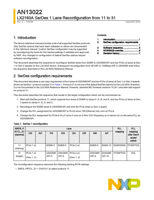
1IntroductionThe device reference manual provides a list of all supported SerDes protocols.Only SerDes options that have been validated on silicon are documented in the reference manual. Custom SerDes configuration may be supported by reconfiguring the lanes for the desired settings if validated and approved by NXP. Any changes to configuration of default SerDes options require software reconfiguration.This document describes the sequence to reconfigure SerDes lanes from SGMII to USXGMII/XFI and two PCIe x2 lanes at Gen 1 or Gen 2 speeds for the LX2160A device. Subsequent reconfiguration from SFI/XFI to 10GBase-KR or USXGMII shall follow the sequence described in the LX2160A Reference Manual.2SerDes configuration requirementsThis document describes a use case requirement of four lanes of USXGMII/XFI and two PCIe x2 lanes at Gen 1 or Gen 2 speeds,shown as SerDes 1 protocol number 31 in Table 1. Protocol 31 is not one of the default SerDes options for the LX2160A, therefore,it is not documented in the LX2160A Reference Manual. However, standard MC firmware versions 10.24.1 and later add support for protocol 31.This document describes the sequence that results in the target configuration which can be summarized as:1.Start with SerDes protocol 11, which supports four lanes of SGMII on lanes F, E, B, and A, and two PCIe x2 lanes at Gen 3 speed on lanes H, G, D, and C.2.Reconfigure the SGMII lanes to USXGMII/XFI and limit the PCIe lanes to Gen 2 speed.3.Change the PLL assignment for USXGMII/XFI to PLLS since 10G Ethernet only runs on PLLS.4.Change the PLL assignment for PCIe to PLLF since it runs on 5 GHz VCO frequency so it cannot run on the same PLL as USXGMII/XFI.Table 1.SerDes 1 reconfigurationThe reconfiguration sequence assumes the following starting RCW settings:•SRDS_PRTCL_S1 = 5'b01011 to select protocol 11.Contents 1Introduction......................................12SerDes configuration requirements ........................................................13Software sequence.........................24RCWSR29 override. (65)Revision history (7)AN13022LX2160A SerDes 1 Lane Reconfiguration from 11 to 31Rev. 0 — 10/2020Application Note•SRDS_DIV_PEX_S1 = 2'b10 to configure PCIe to train up to a max rate of 5G (Gen 2).•SRDS_PLL_REF_CLK_SEL_S1 = 2'b mn, where m selects the reference clock for the PCIe lanes on PLLS and n selects the reference clock for USXGMII/XFI lanes on PLLF. Example:—m = 0 for 100 MHz PCIe reference clock—n = 1 for 161.1328125 MHz USXGMII/XFI reference clock•SRDS_PLL_PD_PLL1 = 0 and SRDS_PLL_PD_PLL2 = 0 so both PLLF and PLLS are powered up.•SRDS_REFCLKF_DIS_S1 = 0 to keep SD1_PLLF_REF_CLK enabled.•SRDS_INTRA_REF_CLK_S1 = 0 intra reference clock is not used.3Software sequenceThe reconfiguration sequence must be implemented in PBI and is shown below.1.Disable SGMII for lanes A, B, E, and F.•SD1: PCC8 (offset 0x10A0) = 0x0000_0000—SGMIIA_CFG = 0 disable SGMIIa—SGMIIB_CFG = 0 disable SGMIIb—SGMIIE_CFG = 0 disable SGMIIe—SGMIIF_CFG = 0 disable SGMIIf2.Enable XFI mode for lanes A, B, E, and F•SD1: PCCC (offset 0x10B0) = 0x9900_9900—SXGMIIA_XFI = 1 PCS operates in XFI/SFI mode—SXGMIIA_CFG = 001b enable SXGMIIa—SXGMIIB_XFI = 1 PCS operates in XFI/SFI mode—SXGMIIB_CFG = 001b enable SXGMIIb—SXGMIIE_XFI = 1 PCS operates in XFI/SFI mode—SXGMIIE_CFG = 001b enable SXGMIIe—SXGMIIF_XFI = 1 PCS operates in XFI/SFI mode—SXGMIIF_CFG = 001b enable SXGMIIf3.Assume 100 MHz reference clock for PLLF for the PCIe lanes•SD1: PLLFCR0 (offset 0x0404) = 0x0000_0000—REFCLK_SEL = 00000b for 100 MHz4.Configure 5G clock net frequency for PLLF•SD1: PLLFCR1 (offset 0x0408) = 0x9030_0008—SLOW_VCO_EN = 1 to enable the slower VCO—FRATE_SEL = 10000b for PCIe on PLLF—HI_BW_SEL = 1 to select higher PLL bandwidth—CLKD_RCAL_SLW_EN = 1 to enable resistor calibration for clock driver—RTMR_BYP = 1 to bypass retimer to clock driver and SSC phase interpolator—EX_DLY_SEL = 00b5.Set the recommended PLLF settings for PCIe 5G•SD1: PLLFCR3 (offset 0x0410) = 0x0000_3000—SSC_SEL = 00b no PLL modulation—SSC_SLP_OFF = 0000000000b for no slope offset—Bit 13 = 1—Bit 12 = 16.Set the recommended PLLF settings for PCIe 5G•SD1: PLLFCR4 (offset 0x0414) = 0x0000_0000—SSC_BIAS_BST = 000b SSC bias boost—SSC_SAW_MIN = 0000000000b SSC minimum sawtooth frequency offset—SSC_PI_BST = 00000b SSC phase interpolator Iqdiv2 boost—SSC_SAW_MAX = 0000000000b SSC maximum sawtooth frequency offset7.Assume 161.1328125 MHz reference clock for PLLS for 10GE operation•SD1: PLLSCR0 (offset 0x0504) = 0x0004_0000—REFCLK_SEL = 00100b for 161.1328125 MHz8.Configure 10.3125G clock net frequency for PLLS•SD1: PLLSCR1 (offset 0x0508) = 0x8610_0008—SLOW_VCO_EN = 1 to enable the slower VCO—FRATE_SEL = 00110b for XFI/SFI on PLLS—HI_BW_SEL = 0 to do not select higher PLL bandwidth—CLKD_RCAL_SLW_EN = 1 to enable resistor calibration for clock driver—RTMR_BYP = 1 to bypass retimer to clock driver and SSC phase interpolator—EX_DLY_SEL = 00b9.Set the recommended PLLS settings for XFI•SD1: PLLSCR3 (offset 0x0510) = 0x0000_3000—SSC_SEL = 00b no PLL modulation—SSC_SLP_OFF = 0000000000b for no slope offset—Bit 13 = 1—Bit 12 = 110.Set the recommended PLLS settings for XFI•SD1: PLLSCR4 (offset 0x0514) = 0x0000_1000—SSC_BIAS_BST = 000b SSC bias boost—SSC_SAW_MIN = 0000000000b SSC minimum sawtooth frequency offset—SSC_PI_BST = 00010b SSC phase interpolator Iqdiv2 boost—SSC_SAW_MAX = 0000000000b SSC maximum sawtooth frequency offset11.Change the PLL assignment for PCIe on the transmitter for lanes C, D, G, H from PLLS to PLLF•SD1: LNmTGCR0 (offsets 0x0A24 for lane C, 0x0B24 for lane D, 0x0E24 for lane G, 0x0F24 for lane H) = 0x0100_0200—USE_SLOW_PLL = 0 transmit uses PLLF—BY_N_RATE_SEL = 001b PCIe is half rate—CM_DLY_MATCH = 1 changes in LNmTRSTCTL[OUT_CM] are delay matched to changes in transmit data 12.Change the PLL assignment for PCIe on the receiver for lanes C, D, G, H from PLLS to PLLF•SD1: LNmRGCR0 (offsets 0x0A44 for lane C, 0x0B44 for lane D, 0x0E44 for lane G, 0x0F44 for lane H) =0x0100_0001—USE_SLOW_PLL = 0 receive uses PLLF—BY_N_RATE_SEL = 001b PCIe is half rate—PTRM_VCM_SEL = 01b Common mode is HiZ if PLLnRST[EN] or LNmRRSTCTL[EN] is negated.13.Change the protocol for lanes A, B, E, F from SGMII to XFI•SD1: LNmGCR0 (offsets 0x0800 for lane A, 0x0900 for lane B, 0x0C00 for lane E, 0x0D00 for lane F) =0x0000_0052—Bit 28 = 0 Must be 0 for all protocols—PORT_LN0_B = 0 Single-lane protocol—PROTO_SEL = 01010b for XFI—IF_WIDTH = 010b 20-bit interface width14.Set the PLL assignment for XFI on the transmitter for lanes A, B, E, F to PLLS•SD1: LNmTGCR0 (offsets 0x0824 for lane A, 0x0924 for lane B, 0x0C24 for lane E, 0x0D24 for lane F) =0x1000_0000—USE_SLOW_PLL = 1 transmit uses PLLS—BY_N_RATE_SEL = 000b 10G is full rate—CM_DLY_MATCH = 0 changes in LNmTRSTCTL[OUT_CM] are not delay matched to changes in transmit data15.Configure the transmit equalization for lanes A, B, E, F for XFI•SD1: LNmTECR0 (offsets 0x0830 for lane A, 0x0930 for lane B, 0x0C30 for lane E, 0x0D30 for lane F) =0x1080_8307—EQ_TYPE = 001b for 2-tap equalization—EQ_SGN_PREQ = 1 for positive sign for pre-cursor—EQ_PREQ = 0000b for 1.0x drive strength of transmit full swing transition bit to pre-cursor—EQ_SGN_POST1Q = 1 for positive sign for first post-cursor—EQ_POST1Q = 00011b for 1.14x drive strength of transmit full swing transition bit to first post-cursor—EQ_AMP_RED = 000111b for 0.585x overall amplitude reduction16.Set the PLL assignment for XFI on the receiver for lanes A, B, E, F to PLLS•SD1: LNmRGCR0 (offsets 0x0844 for lane A, 0x0944 for lane B, 0x0C44 for lane E, 0x0D44 for lane F) =0x1000_0000—USE_SLOW_PLL = 1 receive uses PLLS—BY_N_RATE_SEL = 000b 10G is full rate—PTRM_VCM_SEL = 00b Common mode impedance is always calibrated to SD_GND17.Set the recommended XFI settings for lanes A, B, E, F•SD1: LNmRGCR1 (offsets 0x0848 for lane A, 0x0948 for lane B, 0x0C48 for lane E, 0x0D48 for lane F) =0x1000_0000—RX_ORD_ELECIDLE = 0 Do not put into ordered idle state—Bit 28 = 1—ENTER_IDLE_FLT_SEL = 00b Bypass unexpected entrance into idle—EXIT_IDLE_FLT_SEL = 000b Force immediate exit from idle state AFTER order idle released and min time in idle—DATA_LOST_TH_SEL = 000b Disable loss of signal detection18.Disable receive equalization gain overrides for lanes A, B, E, F•SD1: LNmRECR0 (offsets 0x0850 for lane A, 0x0950 for lane B, 0x0C50 for lane E, 0x0D50 for lane F) =0x0000_000019.Set the recommended the receive equalization for XFI for lanes A, B, E, F•SD1: LNmRECR2 (offsets 0x0858 for lane A, 0x0958 for lane B, 0x0C58 for lane E, 0x0D58 for lane F) =0x8100_0020—Bit 31 = 1—EQ_BLW_SEL = 01b baseline wander for 10G—Bits 5:4 = 10bThe PBI sequence is shown below:.pbiwrite 0x01EA10A0,0x00000000write 0x01EA10B0,0x99009900write 0x01EA0404,0x00000000write 0x01EA0408,0x90300008write 0x01EA0410,0x00003000write 0x01EA0414,0x00000000write 0x01EA0504,0x00040000write 0x01EA0508,0x86100008write 0x01EA0510,0x00003000write 0x01EA0514,0x00001000write 0x01EA0A24,0x01000200write 0x01EA0A44,0x01000001write 0x01EA0B24,0x01000200write 0x01EA0B44,0x01000001write 0x01EA0E24,0x01000200write 0x01EA0E44,0x01000001write 0x01EA0F24,0x01000200write 0x01EA0F44,0x01000001write 0x01EA0800,0x00000052write 0x01EA0900,0x00000052write 0x01EA0C00,0x00000052write 0x01EA0D00,0x00000052write 0x01EA0824,0x10000000write 0x01EA0924,0x10000000write 0x01EA0C24,0x10000000RCWSR29 override write 0x01EA0D24,0x10000000write 0x01EA0830,0x10808307write 0x01EA0930,0x10808307write 0x01EA0C30,0x10808307write 0x01EA0D30,0x10808307write 0x01EA0844,0x10000000write 0x01EA0944,0x10000000write 0x01EA0C44,0x10000000write 0x01EA0D44,0x10000000write 0x01EA0848,0x10000000write 0x01EA0948,0x10000000write 0x01EA0C48,0x10000000write 0x01EA0D48,0x10000000write 0x01EA0850,0x00000000write 0x01EA0950,0x00000000write 0x01EA0C50,0x00000000write 0x01EA0D50,0x00000000write 0x01EA0858,0x81000020write 0x01EA0958,0x81000020write 0x01EA0C58,0x81000020write 0x01EA0D58,0x81000020.end4RCWSR29 overrideThe Reset Configuration Word Status Registers (RCWSR1:RCWSR32) are written with the RCW information that are read from flash memory by the device at power-on-reset. The RCWSR register values are read-only after exiting reset.Software (U-boot) reads the selected SerDes protocol from RCWSR29. It looks at the SerDes configuration table to find the entry for protocol 31 and its corresponding interfaces. In order for software (U-boot) to read the updated SerDes 1 protocol value of 31, the following steps must be performed:1.Add an entry for SerDes 1 protocol 31 in the SerDes configuration table in U-boot2.Override the RCWSR29 with the updated SerDes 1 protocol value of 31•Write to address 0x7_00100170 the new protocol SRDS_PRTCL_S1 = 31.•The SerDes 2 and SerDes 3 configuration fields should remain unchanged.•Note: The RCWSR29 cannot be updated from the PBI phase. The update must be done in the initial stages of the the board-specific U-boot code so that the correct SerDes protocol is read as U-boot continues execution.Table 2.Address 0x7_0010017031302928272625242322212019181716 SRDS_PRTCL_S3SRDS_PRTCL_S2SRDS_PRTCL_S1SRDS_REFCLKF_DIS_S11514131211109876543210Table continues on the next page...Table 2.Address 0x7_00100170 (continued)ReservedSRDS_PLL_P D_PLL6SRDS_PLL_P D_PLL5SRDS_PLL_P D_PLL4SRDS_PLL_P D_PLL3SRDS_PLL_P D_PLL2SRDS_PLL_P D_PLL1Any support, information, and technology (“Materials”) provided by NXP are provided AS IS, without any warranty express or implied, and NXP disclaims all direct and indirect liability and damages in connection with the Material to the maximum extent permitted by the applicable law. NXP accepts no liability for any assistance with applicationsor product design. Materials may only be used in connection with NXP products. Any feedback provided to NXP regarding the Materials may be used by NXP without restriction.5Revision historyThe table below summarizes the revisions to this document.Table 3.Revision history Revision historyHow To Reach Us Home Page: Web Support: /support Information in this document is provided solely to enable system and software implementersto use NXP products. There are no express or implied copyright licenses granted hereunderto design or fabricate any integrated circuits based on the information in this document. NXP reserves the right to make changes without further notice to any products herein.NXP makes no warranty, representation, or guarantee regarding the suitability of its products for any particular purpose, nor does NXP assume any liability arising out of the applicationor use of any product or circuit, and specifically disclaims any and all liability, includingwithout limitation consequential or incidental damages. “Typical” parameters that may be provided in NXP data sheets and/or specifications can and do vary in different applications, and actual performance may vary over time. All operating parameters, including “typicals,”must be validated for each customer application by customer's technical experts. NXP does not convey any license under its patent rights nor the rights of others. NXP sells products pursuant to standard terms and conditions of sale, which can be found at the following address: /SalesTermsandConditions.Security — Customer understands that all NXP products may be subject to unidentifiedor documented vulnerabilities. Customer is responsible for the design and operation of its applications and products throughout their lifecycles to reduce the effect of these vulnerabilities on customer’s applications and products. Customer’s responsibility also extends to other open and/or proprietary technologies supported by NXP products for use in customer’s applications. NXP accepts no liability for any vulnerability. Customer should regularly check security updates from NXP and follow up appropriately. Customer shall select products with security features that best meet rules, regulations, and standards of the intended application and make the ultimate design decisions regarding its products and is solely responsible for compliance with all legal, regulatory, and security related requirements concerning its products, regardless of any information or support that may be provided by NXP. NXP has a Product Security Incident ResponseTeam(PSIRT)(************************)thatmanagestheinvestigation, reporting, and solution release to security vulnerabilities of NXP products.NXP, the NXP logo, Freescale, the Freescale logo, CodeWarrior, Layerscape, and QorIQ are trademarks of NXP B.V. All other product or service names are the property of their respective owners. Arm and Cortex are registered trademarks of Arm Limited (or its subsidiaries) in the US and/or elsewhere. The related technology may be protected by any or all of patents, copyrights, designs and trade secrets. All rights reserved. The Power Architecture and word marks and the Power and logos and related marks are trademarks and service marks licensed by .© NXP B.V. 2020.All rights reserved.For more information, please visit: Forsalesofficeaddresses,pleasesendanemailto:**********************Date of release: 10/2020Document identifier: AN13022。
SD Card SpecificationSimplified Version of:Part E1Secure Digital Input/Output(SDIO)Card SpecificationVersion 1.00October 2001SD AssociationCopyright 2000, 2001 SD AssociationRevision HistoryDate Version Changes compared to previous issueOctober, 2001 1.0 Base version initial releaseConditions for publicationPublisher and Copyright Holder:SD Association719 San Benito St. Suite CHollister, CA 95023USAPhone: +1 831 636 7322Fax: +1 831 623 2248E-mail: president@Confidentiality:This document is a simplified version of the original. This version is not required to be treated as confidential and Non Disclosure Agreement with neither the 3C LLC nor the SDA is required.Reproduction in whole or in part is prohibited without prior written permission of SDA.Exemption:None will be liable for any damages from use of this document.Important additional information!The reader is directed to the additional information available in section Error! Reference source not found.. This information will inform the reader of changes to the SDIO specification proposed for the next revision of this specification that should be considered in the design of any SDIO device.Table of Contents1.General Description (1)1.1SDIO features (1)1.2Primary Reference Document (1)2.SDIO Signaling Definition (2)2.1SDIO Card Types (2)2.2SDIO Card modes (2)2.2.1SPI (Card mandatory support) (2)2.2.21-bit SD data transfer mode (Card mandatory support) (2)2.2.34-bit SD data transfer mode (mandatory for High-Speed cards, optional for Low-Speed) (2)2.3SDIO Host Modes (2)2.4Signal Pins (3)2.5Host Requirements for SDIO (3)3.SDIO Card Initialization (4)3.1Differences in I/O card initialization (4)4.Differences with SD Memory Specification (7)4.1Unsupported SD Memory commands (7)4.2Bus Width (8)4.3Card Detect Resistor (8)4.4Data Transfer Abort (8)4.5Changes to SD Memory Fixed Registers (8)4.5.1OCR Register (8)4.5.2CID Register (8)4.5.3RCA Register (8)5.New I/O Read/Write Commands (9)5.1IO_RW_DIRECT command (CMD52) (9)5.2IO_RW_EXTENDED command (CMD53) (9)5.2.1CMD53 Data Transfer Format (9)6.SDIO Card Internal Operation (10)6.1Overview (10)6.2Register Access Time (10)6.3Interrupts (10)6.4Suspend/Resume (11)6.5Read Wait (Optional) (11)6.6SDIO Fixed Internal Map (12)6.7Common I/O Area (CIA) (12)6.8Card Common Control Registers (CCCR) (13)6.9Function Basic Registers (FBR) (13)6.10Card Information Structure (CIS) (13)6.11Multiple Function SD Cards (13)6.12Embedded I/O Code Storage Area (CSA) (13)7.SDIO Interrupts (14)7.1Interrupt Timing (14)7.1.1SPI and SD 1-bit mode interrupts (14)7.1.2SD 4-bit mode (14)7.1.3Interrupt Clear Timing (14)8.SDIO Physical Properties (15)8.1SDIO Size (15)8.2SDIO Card Package (15)9.SDIO Mechanical Extensions (16)9.1Additional ESD/EMI Ground Point (16)9.2Extended Case (16)9.3Write Protect Switch (16)10.SDIO Power (18)10.1SDIO Card Initialization Voltage (18)10.2SDIO Power Consumption (18)10.3SDIO Current (18)11.Abbreviations and Terms (19)A.1SD and SPI Command List........................................................................................................................AB.1Normative References..............................................................................................................................CC.1Example SDIO Controller Design.............................................................................................................DTable of TablesTable 1 SDIO pin definitions (3)Table 2 Unsupported SD Memory Commands (7)Table 3 SDIO exceptions to SD physical section 8.1 requirements (15)Table 4 SD Mode Command List..........................................................................................................................A Table 5 SPI Mode Command List.........................................................................................................................BTable of FiguresFigure 1 Signal connection to two 4-bit SDIO cards (3)Figure 2 Card initialization flow in SD mode (SDIO aware host) (5)Figure 3 Card initialization flow in SPI mode (SDIO aware host) (6)Figure 4 SDIO Internal Map (12)Figure 5 SDIO Mechanical Extensions (17)Figure 6 SDIO Internal State Machine example..................................................................................................D Figure 7 State Diagram for Bus State Machine...................................................................................................D Figure 8 State Diagram for Function State Machine.............................................................................................E1. GeneralDescriptionThe SDIO (Secure Digital I/O) card is based on and compatible with the SD memory card. This compatibility includes mechanical, electrical, power, signaling and software. The intent of the SDIO card is to provide high-speed data I/O with low power consumption for mobile electronic devices. A primary goal is that an SDIO card inserted into a non-SDIO aware host will cause no physical damage or disruption of that device or it’s software. In this case, the SDIO card should simply be ignored. Once inserted into an SDIO aware host, the detection of the card will be via the normal means described in the SD specification with some extensions. In this state, the SDIO card will be idle and draw a small amount of power (15 mA averaged over 1 second). During the normal initialization and interrogation of the card by the host, the card will identify itself as an SDIO device. The host software will then obtain the card information in a tuple (linked list) format and determine if that card’s I/O function(s) are acceptable to activate. This decision will be based on such parameters as power requirements or the availability of appropriate software drivers. If the card is acceptable, it will be allowed to power up fully and start the I/O function(s) built into it.features1.1 SDIOTargeted for portable and stationary applicationsMinimal or no modification to SD Physical bus is requiredMinimal change to memory driver softwareExtended physical form factor available for specialized applicationsPlug and play (PnP) supportMulti-function support including multiple I/O and combined I/O and memoryUp to 7 I/O functions plus one memory supported on one card.Allows card to interrupt hostInitialization Voltage: 2.0 to 3.6VOperational Voltage range: 3.1 to 3.5V1.2 Primary Reference DocumentThis spec is based on and refers extensively to the SDA document:SD Memory Card SpecificationsPart 1PHYSICAL LAYER SPECIFICATIONSeptember 2000Version 1.01The reader is directed to this document for more information on the basic operation of SD devices. In addition, other documents are referenced in this specification. A complete list can be found in section B.1.2. SDIO Signaling Definition2.1 SDIO Card TypesThis specification defines two types of SDIO cards. The Full-Speed card supports SPI, 1-bit SD and the 4-bit SD transfer modes at the full clock range of 0-25MHz. The Full-Speed SDIO devices have a data transfer rate of over 100 Mb/second (10 MB/Sec). A second version of the SDIO card is the Low-Speed SDIO card. This card requires only the SPI and 1-bit SD transfer modes. 4-bit support is optional. In addition, Low-Speed SDIO cards shall support a full clock range of 0-400 KHz. The intended use of Low-Speed cards is to support low-speed IO devices with a minimum of hardware. The Low-Speed cards support such functions as modems, bar-code scanners, GPS receivers etc. If a card is a ‘Combo card’ (memory plus SDIO) then Full-Speed and 4-bit operation is mandatory for both the memory and SDIO portions of the card.2.2 SDIO Card modesThere are 3 signaling modes defined for SD physical specification version 1.01 memory cards that also apply to SDIO Card:2.2.1 SPI (Card mandatory support)The SPI bus topology is defined in section 3.1.2 and the protocol is defined in sections 3.2.2 and 7 of the SD Memory Card Specifications, PHYSICAL LAYER SPECIFICATION, Part 1,September 2000 Version1.01. In this mode pin 8, which is undefined for memory, is used as the interrupt pin. All other pins andsignaling protocols are identical to the SD Memory specification.2.2.2 1-bit SD data transfer mode (Card mandatory support)This mode is identical to the 1 data bit (narrow) mode defined for SD Memory in section 3.2.1 of the SD Memory Card specification. In this mode, data is transferred on the DAT[0] pin only. In this mode pin 8, which is undefined for memory, is used as the interrupt pin. All other pins and signaling protocols are identical to the SD Memory specification.2.2.3 4-bit SD data transfer mode (mandatory for High-Speed cards, optional for Low-Speed)This mode is identical to the 4 data bit mode (wide) defined for SD Memory in section 3.2.1 of the SD Memory Card specification. In this mode, data is transferred on all 4 data pins (DAT[3:0]). In this mode the interrupt pin is not available for exclusive use as it is utilized as a data transfer line. Thus, if the interrupt function is required, a special timing is required to provide interrupts. See section 7.1.2 for details of this Modes2.3 SDIOHostIf a SDIO aware host supports the SD transfer mode, it is recommended that both the 1-bit and 4-bit modes be supported. While a SDIO host that supports only the 4-bit transfer mode is possible, it’s performance with a Low-Speed SDIO card would be reduced. This is because the only means to transfer data to and from a Low-Speed card would be the single byte per command transfer (using the IO_RW_DIRECT command (CMD52) see 5.1).2.4 Signal PinsFigure 1 Signal connection to two 4-bit SDIO cardsPin SD 4-bit mode SD 1-bit mode SPI mode 1 CD/DAT[3] Data line 3 N/C Not Used CSCard Select 2 CMD Command line CMD Command line DI Data input 3 VSS1 Ground VSS1 Ground VSS1 Ground 4 VDD Supply voltage VDD Supply voltage VDD Supply voltage 5 CLK Clock CLK Clock SCLK Clock 6 VSS2 Ground VSS2 Ground VSS2 Ground 7 DAT[0] Data line 0 DATA Data line DO Data output 8 DAT[1] Data line 1 or Interrupt (optional)IRQ Interrupt IRQ Interrupt9 DAT[2] Data line 2 or Read Wait (optional)RW Read Wait (optional) NC Not UsedTable 1 SDIO pin definitionsIt is recommended that multi-slot hosts intending to support SDIO (SDIO aware) provide a separate CLK to each slot, to allow the I/O devices to be placed in a low power state on a slot-by-slot basis. After reset, all data lines (DAT[3:0]) shall be in the hi-Z state on both the host and card(s) to avoid bus conflict. Access to the Bus Interface Control register within the CCCR determines DAT line mode.2.5 Host Requirements for SDIOIn order for a host to completely support all of the capabilities of the SDIO cards, some signal connections must be supported. In order to support interrupts, the host shall have Pin 8 connected from the card to the host in order to provide interrupt signaling. This is true even if the host will only support the SPI or 1 bit SD mode. In addition, if the host supports more than 1 card in either SD mode, the CMD and all 4 data lines (DAT[3:0]) should not be bussed together, but rather routed separately to the host. This will allow the mixing of card types in the different sockets without interference. Both the SD Memory specification and the SDIO specification support the concept of “unifying” (connecting together) the CMD lines in a multi-slot system after initialization.3. SDIO Card Initialization3.1 Differences in I/O card initializationA requirement for the SDIO specification is that an SDIO card must not cause non-I/O aware hosts to fail when inserted. In order to prevent operation of I/O Functions in non-I/O aware hosts, a change to the SD card identification mode flowchart is needed. A new command (IO_SEND_OP_COND, CMD5) is added to replace the ACMD41 for SDIO initialization by I/O aware hosts.After reset or power-up, all I/O functions on the card are disabled and the I/O portion of the card will not respond to any operation except CMD5 or CMD0 with CS=low. If there is SD memory installed on the card (also called a combo card), that memory will respond normally to all normal mandatory memory commands.An I/O only card will not respond to the ACMD41 and thus appear initially as an MMC card (See B.1 forthe MMC cards and appear as a non-responsive card. The host will then give up and disable this device Thus, the non-aware host will receive no response from an I/O only card and force it to the inactive state.An SDIO aware host will send CMD5 prior to the CMD55/ACMD41 pair, and thus would receive a valid OCR in the R4 response to CMD5 and continue to initialize the card. Figure 2 shows the operation of an SDIO aware host operating in the SD modes and Figure 3 shows the same operation for a host that operates in the SPI mode.If the I/O portion of a card has received no CMD5, the I/O section remains inactive and will not respond to any command except CMD5. A combo card stays in the memory-only mode. If no memory is installed on the card (i.e. an I/O only card in a non-SDIO aware host) the card would not respond to any memory command. This satisfies the condition where a user uses some I/O function on the card such as Ethernet to load a music file to the memory function of that card. The card is then removed and inserted into a non-SDIO aware host. That device would not enable the I/O function (no CMD5) so would appear to the player as a memory-only card. If the host were I/O aware, it would send the CMD5 to the card and the card would respond with R4. The host reads that R4 value and knows the number of available I/O functions and about the existence of any SD memory.The function of CMD5 for SDIO cards is similar to the operation of ACMD41 for SD memory cards. It is used to inquire about the voltage range needed by the I/O card. The normal response to CMD5 is R4 in either SD or SPI format. The I/O aware host will send CMD5. If the card responds with response R4, the host determines the card’s configuration based on the data contained within the R4.After the host has initialized the I/O portion of the card, it then reads the Common Information Area (CIA) of the card (see 6.7). This is done by issuing a read command, starting at byte 00 of I/O function 0. The CIA contains CIA are pointers to the card’s common Card Information Structure (CIS) and each individual function’s CIS. The CIS includes information on power, function, manufacturer and other things the host needs to determine if the I/O function(s) is appropriate to power-up. If the host determines that the card should be activated, a register in the CCCR area enables the card and each individual function. At this time, all functions of the I/O card are fully available. In addition, the host can control the power consumption and enable/disable interrupts on a function-by-function basis. This access to I/O will not interfere with memory access to the card if present.Figure 2 Card initialization flow in SD mode (SDIO aware host)IO =1, M E M =0IO =1, M E M =1c tio n s s is re ad y (C s ta tu s is lize d fla g fla g g (in th e5)a tio n R e s p o n s eM P =0, IO =0S ta rt in itia liz a tio n w ith C M D 0, C M D 1IO =0, M E M =1{IO=0, MEM=0, PI=0}IO=0, MEM=0Start initialization withCMD0 and CMD1Figure 3 Card initialization flow in SPI mode (SDIO aware host)4. Differences with SD Memory Specification4.1 Unsupported SD Memory commandsSeveral commands required for SD Memory devices are not supported by either SDIO-only cards or the I/O portion of Combo cards. Some of these commands have no use in SDIO devices such as Erase commands and thus are not supported in SDIO. In addition, there are several commands for SD memory cards that have different commands when used with the SDIO section of a card. Table 2 lists these SD Memory commands and the equivalent SDIO commands. For a complete list of supported and unsupported commands, see Table 4 and Table 5.Table 2 Unsupported SD Memory Commands4.2 BusWidthFor a SD memory card, the bus width for SD mode is set using ACMD6. The SDIO card uses a write to the CCCR using CMD52 to select bus width. In the case of a combo card, both selection methods exist. In this case, the host shall set the bus width in both locations by issuing both the ACMD6 and the CCCR write using CMD52 with the same width before starting any data transfers. Note that Low-Speed SDIO cards support 4-bit transfer as an option. When communication with a Low-Speed SDIO card, the host must first determine if the card supports 4-bit transfer prior to attempting to select that mode.4.3 Card Detect ResistorSD memory and I/O cards use a pull-up resistor on DAT[3] to detect card insertion. The procedure to enable/disable this resistor is different between SD memory and SDIO. SD memory uses ACMD42 to control this resistor while SDIO uses writes to the CCCR using CMD52. In the case of a combo card, both control locations exist and must be managed by the host. For a combo card, the resistor is enabled unless both the memory and the I/O control registers have the resistor disabled. After power-up, both locations default to resistor enabled. Note that after an I/O reset, the I/O resistor enable is not changed.Abort4.4 DataTransferA host communicating with a SD memory device uses CMD12 to abort the transfer of read or write data to/from the card. For an SDIO device, CMD12 abort is replaced by a write to the ASx bits in the CCCR. Normally, the abort is used to stop an infinite block transfer (block count=0). If an exact number of blocks to be transferred, it is recommended that the host issue a block command with the correct block count, rather than using an infinite count and aborting the data at the correct time.4.5 Changes to SD Memory Fixed RegistersRegister4.5.1 OCRAll SD cards (memory, I/O and combo) shall have at least one OCR register. If the card is a combo card, it may have two OCR’s (one for memory and one for I/O). The memory portion of a combo card has an OCR accessed using ACMD41 and CMD58. The I/O portion of a card has an OCR with the same structure that is accessed via CMD5. If there are multiple OCR’s the voltage range may not be identical. Some I/O functions may have a wider VDD range than that reflected in the I/O OCR register. The I/O OCR will be the logical AND of the voltage ranges(s) of all I/O functions. Note that the I/O OCR format is different from the memory version in that it is only 24 bits long. The per-function voltage for each I/O function can be read in the CIS for the card.Register4.5.2 CIDThere shall be a maximum of one CID register per SD card. If the card contains both memory and I/O, the CID register information is unchanged from the SD 1.01 version and reflects the information from the memory portion of the card. If the card is I/O only, the CID register and the associated access command (CMD10) are not supported. If the host attempts to access this register in an I/O only device, a card in SPI mode will respond with an "Invalid Command" error response and a card in SD mode will not respond.Register4.5.3 RCAThere shall only be one RCA register per SD card. The RCA value shall apply to the card as a whole. All functions and any memory share the same card address.5. New I/O Read/Write CommandsTwo additional data transfer instructions have been added to support I/O. IO_RW_DIRECT, a direct I/O command similar to the MMC 'Fast I/O' command, and IO_RW_EXTENDED, which allows fast access with byte or block addresses. Both commands are in class 9 (I/O Commands).5.1 IO_RW_DIRECT command (CMD52)The IO_RW_DIRECT is the simplest means to access a single register within the total 128K of register space in any I/O function, including the common I/O area (CIA). This command reads or writes 1 byte using only 1 command/response pair. A common use is to initialize registers or monitor status values for I/O functions. This command is the fastest means to read or write single I/O registers, as it requires only a single command/response pair.The SDIO card’s response to CMD52 will be in one of two formats. If the communication between the card and host is in the 1-bit or 4-bit SD mode, the response will be in a 48-bit response (R5). If the communication is using the SPI mode, the response will be a 16-bit R5 response.5.2 IO_RW_EXTENDED command (CMD53)In order to read and write multiple I/O registers with a single command, a new command, IO_RW_EXTENDED is defined. This command is included in command class 9 (I/O Commands). This command allows the reading or writing of a large number of I/O registers with a single command. Since this is a data transfer command, it provides the highest possible transfer rate.The response from the SDIO card to CMD53 will be R5 (the same as CMD52). For CMD53, the 8-bit data field will be stuff bits and shall be read as 0x00.5.2.1 CMD53 Data Transfer FormatWhen executing the IO_RW_EXTENDED (CMD53), the multi-byte or multi-block data transfer is similar to the data transfer for memory. For the multi-byte transfer modes (block mode=0) the following applies:IO_RW_EXTENDED byte read is similar to CMD17 (READ_SINGLE_BLOCK)IO_RW_EXTENDED byte write is similar to CMD24 (WRITE_BLOCK)Note that the byte count for this transfer is set in the command, rather than the fixed block size. Thus, the size of the data payload will be in the range of 1-512 bytes. The block mode is similar to the following memory commands:IO_RW_EXTENDED block read is similar to CMD18 (READ_MULTIPLE_BLOCK)IO_RW_EXTENDED block write is similar to CMD25 (WRITE_MULTIPLE_BLOCK)For the block mode the only difference is that for a fixed block count, the host does not need to stop the transfer, as it will continue until the block count is satisfied. If the block count is set to zero, the operation is identical to the memory mode in that the host must stop the transfer.6. SDIO Card Internal OperationI/O access differs from memory in that the registers can be written and read individually and directly without a FAT file structure or the concept of blocks (although block access is supported). These registers allow access to the I/O data, control of the I/O function and report on status or transfer I/O data to/from the host. The SD memory relies on the concept of a fixed block length with commands reading/writing multiples of these fixed size blocks. I/O may or may not have fixed block lengths and the read size may be different from the write size. Because of this, I/O operations may be based on either a length (byte count) or a block size.6.1 OverviewEach SDIO card may have from 1 to 7 functions plus one memory function built into it. A function is a self contained I/O device. I/O functions may be identical or completely different from each other. All I/O functions are organized as a collection of registers. There is a maximum of 131,072 (217) registers possible for each I/O function. These registers and their individual bits may be read Only (RO), Write Only (WO) or Read/Write (R/W). These registers can be 8, 16 or 32 bits wide within the card. All addressing is based on byte access. These registers can be written and/or read one at a time, multiply to the same address or multiply to an incrementing address. The single R/W access is often used to initialize the I/O function or to read a single status or data value. The multiple reads to a fixed address are used to read or write data from a data FIFO register in the card. The read to incrementing addresses is used to read or write a collection of data to/from a RAM area inside of the card. Figure 4 shows the mapping of the CIA and optional CSA space for an SDIO card.Time6.2 RegisterAccessAll registers in SDIO only cards and the SDIO portion of Combo cards must complete read and write data transfer in less than 1 second. The host can use 1 second as the timeout value for a non-responding location. If a functions needs to support an access time greater than 1 second, the card maker will use some function specific method that is not defined in this specification. The 1-second response time is dependant on the SDCLK frequency. If the Average frequency of the SDCLK is less than 100KHz then the card may not be able to respond within the 1-second limit. The host should adjust the timeout in the case the average frequency of the SDCLK is less than 100KHz.6.3 InterruptsAll SDIO hosts shall support interrupts in both the SPI and 1-bit SD modes. Each function within an SDIO or Combo card may implement interrupts as needed. The interrupt used on SDIO functions is a type commonly called “level sensitive”. Level sensitive means that any function may signal for an interrupt at any time, but once the function has signaled an interrupt, it will not release (stop signaling) the interrupt until the cause of the interrupt is removed or commanded to do so by the host. Since there is only 1 interrupt line, it may be shared by multiple interrupt sources. The function shall continue to signal the interrupt until the host responds and clears the interrupt. Since multiple interrupts may be active at once, it is the responsibility of the host to determine the interrupt source(s) and deal with it as needed. This is done on the SDIO function by the use of two bits, the interrupt enable and interrupt pending. Each function that may generate an interrupt has an interrupt enable bit. In addition, the SDIO card has a master interrupt enable that controls all functions. An interrupt will only be signaled to the SD bus if both the function’s enable and the card’s master enable are set. The second interrupt bit is called interrupt pending. This read-only bit tells the host which function(s) may be signaling for an interrupt. There is an interrupt pending bit for each function that can generate interrupts. These bits are located in the CCCR area.6.4 Suspend/ResumeWithin a multi-function SDIO or a Combo card, there are multiple devices (I/O and memory) that must share access to the SD bus. In order to allow the sharing of access to the host among multiple devices, SDIO and combo cards can implement the optional concept of suspend/resume. If a card supports suspend/resume, the host may temporarily halt a data transfer operation to one function or memory (suspend) in order to free the bus for a higher priority transfer to a different function or memory. Once this higher-priority transfer is complete, the original transfer is re-started where it left off (resume). Support of suspend/resume is optional on a per-card basis. If suspend/resume is implemented, it shall be supported by the memory (if any) of a Combo card and all I/O functions except 0 (the CIA). Note that the host can suspend multiple transactions and resume them in any order desired. I/O function 0 does not support suspend/resume. Note that Suspend/Resume is defined only for the SD 1 and 4-bit modes. It does not apply to SPI transfers.6.5 Read Wait (Optional)Host devices built to the SD Physical specification version 1.01 must control the SDCLK to stop the read data block output from a card executing a multiple read command whenever the host cannot accept more data. During the time that the host has stopped the SDCLK, a CMD52 cannot be issued. This limitation causes a problem in that a host device built to the SD Physical specification version 1.01 cannot perform the I/O command during a multiple read cycle.In order to eliminate this limitation, the SDIO specification adds the read wait control to enable the host to issue CMD52 during a multiple read cycle. Read Wait uses the DAT[2] line to allow the host to signal the card to temporarily halt the sending of read data by a card. This feature is optional for an SDIO or combo card. However, if an SDIO or combo supports Read Wait, all functions and any memory must support read wait. Note that Read Wait is defined only for the SD 1 and 4-bit modes. It does not apply to SPI transfers.To determine if a card supports the Read Wait protocol, the host must test SRW capability bit in the Card Capability byte of the CCCR. If a card does not support the Read Wait protocol, the only means a host has to stall (not abort) data in a read multiple command is to control the SDCLK.。
Technical Committee SD Card AssociationRevision HistoryDate Version Changes compared to previous issueApril 3, 2006 1.10 The first release of the SDIO Simplified SpecificationFebruary 8, 2007 2.00 Followings functions are added in this version(1) Added method to change bus speed (Normal Speed up to 25MHz andHigh Speed up to 50 MHz)(2) Operational Voltage Requirement is extended to 2.7-3.6V(3) Combine sections 12 (Physical Properties) and 13 (MechanicalExtensions) and add miniSDIO to the new section 13 (PhysicalProperties)(4) Add Embedded SDIO ATA Standard Function Interface Code(5) Reference of Physical Ver2.00 supports SDHC combo card.(6) Some typos in Ver1.10 are fixed.February 25, 2011 3.00 Followings functions are added in this version(1) Definition of Embedded SDIO(2) Ultra High Speed Bus Speed Mode (UHS-I)(3) Power Control Extension (Power State Control)(4) Asynchronous Interrupt in 4-bit mode(5) Shared Bus for supporting multiple devices(6) Interface Signal of Embedded Device applicable to Shared BusAsynchronous Interrupt is not included in this document.Release of SD Simplified SpecificationThe following conditions apply to the release of the SD simplified specification ("Simplified Specification") by the SD Card Association. The Simplified Specification is a subset of the complete SD Specification which is owned by the SD Card Association.Publisher and Copyright Holder:SD Card Association2400 Camino Ramon, Suite 375San Ramon, CA 94583 USATelephone: +1 (925) 275-6615,Fax: +1 (925) 886-4870E-mail: office@Notes:This Simplified Specification is provided on a non-confidential basis subject to the disclaimers below. Any implementation of the Simplified Specification may require a license from the SD Card Association or other third parties.Disclaimers:The information contained in the Simplified Specification is presented only as a standard specification for SD Cards and SD Host/Ancillary products and is provided "AS-IS" without any representations or warranties of any kind. No responsibility is assumed by the SD Card Association for any damages, any infringements of patents or other right of the SD Card Association or any third parties, which may result from its use. No license is granted by implication, estoppel or otherwise under any patent or other rights of the SD Card Association or any third party. Nothing herein shall be construed as an obligation by the SD Card Association to disclose or distribute any technical information, know-how or other confidential information to any third party.Conventions Used in This DocumentNaming Conventions•Some terms are capitalized to distinguish their definition from their common English meaning. Words not capitalized have their common English meaning.Numbers and Number Bases•Hexadecimal numbers are written with a lower case "h" suffix, e.g., FFFFh and 80h.•Binary numbers are written with a lower case "b" suffix (e.g., 10b).•Binary numbers larger than four digits are written with a space dividing each group of four digits, as in 1000 0101 0010b.•All other numbers are decimal.Key Words•May: Indicates flexibility of choice with no implied recommendation or requirement.•Shall: Indicates a mandatory requirement. Designers shall implement such mandatory requirements to ensure interchangeability and to claim conformance with the specification.•Should: Indicates a strong recommendation but not a mandatory requirement. Designers should give strong consideration to such recommendations, but there is still a choice in implementation. Application NotesSome sections of this document provide guidance to the host implementers as follows:Application Note:This is an example of an application note.Table of Contents1. General Description (1)1.1 Definitions (1)1.1.1 SDIO Card (1)1.1.2 Embedded SDIO (1)1.2 SDIO Features (1)1.2.1 Common SDIO Features (1)1.2.2 SDIO Card Features (1)1.2.3 Embedded SDIO Device Features (2)1.3 Document Structure (3)1.4 Standard SDIO Functions (3)2. SDIO Signaling Definition (4)2.1 SDIO Card Types (4)2.2 SDIO Card Modes (4)2.2.1 SPI (Card mandatory support) (4)2.2.2 1-bit SD Data Transfer Mode (Card Mandatory Support) (4)2.2.3 4-bit SD Data Transfer Mode (Mandatory for High-Speed Cards, Optional for Low-Speed) (4)2.3 SDIO Host Modes (4)2.4 Signal Pins (5)2.4.1 Signal Pins for SDIO Card (5)3. SDIO Card Initialization (6)3.1 Initialization Sequence (6)3.1.1 Initialization by Non-I/O Aware Host (6)3.1.2 Initialization by I/O Aware Host (7)3.2 The IO_SEND_OP_COND Command (CMD5) (13)3.3 The IO_SEND_OP_COND Response (R4) (14)3.4 Special Initialization Considerations for Combo Cards (15)3.4.1 Re-initialize Both I/O and Memory (15)3.4.2 Using a Combo Card as SDIO only or SD Memory only after Combo Initialization (15)3.4.3 Acceptable Commands after Initialization (15)3.4.4 Recommendations for RCA after Reset (15)3.4.5 Enabling CRC in SPI Combo Card (17)4. Differences with SD Memory Specification (18)4.1 SDIO Command List (18)4.2 Memory Commands and SDIO Commands (18)4.2.1 Supported SD Memory Commands (18)4.2.2 Unsupported SD Memory Commands (18)4.3 Modified R6 Response (19)4.4 Reset for SDIO (20)4.5 Bus Width (20)4.6 Card Detect Resistor (20)4.7 Timings (21)4.8 Data Transfer Block Sizes (21)4.9 Data Transfer Abort (21)4.9.1 Read Abort (21)4.9.2 Write Abort (21)4.10 Changes to SD Memory Fixed Registers (22)4.10.1 OCR Register (22)4.10.2 CID Register (22)4.10.3 CSD Register (22)4.10.4 RCA Register (22)4.10.5 DSR Register (22)4.10.6 SCR Register (23)4.10.7 SD Status (23)4.10.8 Card Status Register (23)5. New I/O Read/Write Commands (25)5.1 IO_RW_DIRECT Command (CMD52) (25)5.2 IO_RW_DIRECT Response (R5) (26)5.2.1 CMD52 Response (SD Modes) (26)5.2.2 R5, IO_RW_DIRECT Response (SPI mode) (27)5.3 IO_RW_EXTENDED Command (CMD53) (28)5.3.1 CMD53 Data Transfer Format (29)5.3.2 Special Timing for CMD53 Multi-Block Read (29)6. SDIO Card Internal Operation (30)6.1 Overview (30)6.2 Register Access Time (30)6.3 Interrupts (30)6.4 Suspend/Resume (31)6.5 Read Wait (31)6.6 CMD52 During Data Transfer (31)6.7 SDIO Fixed Internal Map (31)6.8 Common I/O Area (CIA) (32)6.9 Card Common Control Registers (CCCR) (32)6.10 Function Basic Registers (FBR) (43)6.11 Card Information Structure (CIS) (46)6.12 Multiple Function SDIO Cards (46)6.13 Setting Block Size with CMD53 (46)6.14 Bus State Diagram (47)7. Embedded I/O Code Storage Area (CSA) (48)7.1 CSA Access (48)7.2 CSA Data Format (48)8. SDIO Interrupts (49)8.1 Interrupt Timing (49)8.1.1 SPI and SD 1-bit Mode Interrupts (49)8.1.2 SD 4-bit Mode (49)8.1.3 Interrupt Period Definition (49)8.1.4 Interrupt Period at the Data Block Gap in 4-bit SD Mode (Optional) (49)8.1.5 End of Interrupt Cycles (49)8.1.6 Terminated Data Transfer Interrupt Cycle (50)8.1.7 Interrupt Clear Timing (50)8.2 Asynchronous Interrupt (50)9. SDIO Suspend/Resume Operation (51)10. Timing to Pause SDIO Read Operation (52)10.1 Pause Read Operation by Stopping SDCLK (52)10.2 Pause Read Operation by using Read Wait (52)11. Power Control (53)11.1 Power Control Overview (53)11.2 Details of SDIO Power Control (53)11.2.1 Master Power Control (53)11.2.2 Power Selection (54)11.2.3 Power State Control (54)11.2.4 High-Power Tuples (54)11.2.5 The Maximum Card Power Restricted by Tc (55)11.3 Power Control Support for the SDIO Host (56)11.3.1 Version 1.10 Host (56)11.3.2 Version 3.00 Host (56)12. High-Speed Mode (57)12.1 SDIO High-Speed Mode (57)12.2 Switching Bus Speed Mode in a Combo Card (57)13. SDIO Physical Properties (58)13.1 SDIO Form Factors (58)13.2 Full-Size SDIO (58)13.3 miniSDIO (58)13.4 microSDIO (58)14. SDIO Power (59)14.1 SDIO Card Initialization Voltages (59)14.2 SDIO Power Consumption (59)15. Inrush Current Limiting (60)16. CIS Formats (61)16.1 CIS Reference Document (61)16.2 Basic Tuple Format and Tuple Chain Structure (61)16.3 Byte Order Within Tuples (61)16.4 Tuple Version (62)16.5 SDIO Card Metaformat (62)16.6 CISTPL_MANFID: Manufacturer Identification String Tuple (63)16.7 SDIO Specific Extensions (63)16.7.1 CISTPL_FUNCID: Function Identification Tuple (63)16.7.2 CISTPL_FUNCE: Function Extension Tuple (63)16.7.3 CISTPL_FUNCE Tuple for Function 0 (Extended Data 00h) (64)16.7.4 CISTPL_FUNCE Tuple for Function 1-7 (Extended Data 01h) (65)16.7.5 CISTPL_FUNCE Tuple for Function 1-7 (Extended Data 02h) (68)16.7.6 CISTPL_SDIO_STD: Function is a Standard SDIO Function (69)16.7.7 CISTPL_SDIO_EXT: Tuple Reserved for SDIO Cards (70)17. Embedded SDIO (71)17.1 Relaxing SDIO Requirements for Embedded Device (71)17.1.1 Form Factor (71)17.1.2 CIS Information (71)17.1.3 8-Bit Bus Mode (71)17.2 Interface Signal for Embedded SDIO Device (71)17.3 Shared Bus Configuration (71)Appendix A (Normative) : Reference (73)A.1 Reference (73)Appendix B (Normative) : Special Terms (74)B.1 Terminology (74)B.2 Abbreviations (74)Appendix C (Normative) : Command List (76)C.1 SD Mode Command List (76)C.2 SPI Mode Command List (77)Appendix D (Normative) (78)Table of TablesTable 3-1 : OCR Values for CMD5 (13)Table 4-1 : Supported SD Memory Commands (18)Table 4-2 : Unsupported SD Memory Commands (19)Table 4-3 : R6 response to CMD3 (19)Table 4-4 : SDIO R6 Status Bits (19)Table 4-5 : Combo Card 4-bit Control (20)Table 4-6 : Card Detect Resistor States (21)Table 4-7 : SDIO Status Register Structure (24)Table 5-1 : Flag Data for IO_RW_DIRECT SD Response (27)Table 5-2 : IO_RW_ EXTENDED command Op Code Definition (28)Table 5-3 : Byte Count Values (29)Table 6-1 : Card Common Control Registers (CCCR) (33)Table 6-2 : CCCR bit Definitions (42)Table 6-3 : Function Basic Information Registers (FBR) (43)Table 6-4 : FBR bit and field definitions (45)Table 6-5 : Card Information Structure (CIS) and reserved area of CIA (46)Table 11-1 : Reference of Tuples Depends on Host Version (55)Table 16-1 : Basic Tuple Format (61)Table 16-2 : Tuples Supported by SDIO Cards (62)Table 16-3 : CISTPL_MANFID: Manufacturer Identification Tuple (63)Table 16-4 : CISTPL_FUNCID Tuple (63)Table 16-5 : CISTPL_FUNCE Tuple General Structure (64)Table 16-6 : TPLFID_FUNCTION Tuple for Function 0 (Common) (64)Table 16-7 : TPLFID_FUNCTION Field Descriptions for Function 0 (common) (65)Table 16-8 : TPLFID_FUNCTION Tuple for Function 1-7 (High Power Tuple) (66)Table 16-9 : TPLFID_FUNCTION Field Descriptions for Functions 1-7 (68)Table 16-10 : TPLFE_FUNCTION_INFO Definition (68)Table 16-11 : TPLFE_CSA_PROPERTY Definition (68)Table 16-12 : TPLFID_FUNCTION Tuple for Function 1-7 (Power State Tuple) (68)Table 16-13 : TPLFID_FUNCTION Field Descriptions for Functions 1-7 (Power State Tuple) (69)Table 16-14 : CISTPL_SDIO_STD: Tuple Reserved for SDIO Cards (69)Table 16-15 : TPL_CODE CISTPL_SDIO_STD Definition (69)Table 16-16 : CISTPL_SDIO_EXT: Tuple Reserved for SDIO Cards (70)Table C- 1 : SD Mode Command List (76)Table C- 2 : SPI Mode Command List (77)©Copyright 2000-2011 SD Card Association SDIO Simplified Specification Version 3.00Table of FiguresFigure 1-1 : SDIO Related Specifications (3)Figure 2-1 : Signal connection to two 4-bit SDIO cards (5)Figure 3-1 : SDIO Response to Non-I/O Aware Initialization (6)Figure 3-2 : Card Initialization Flow in SD mode (SDIO Aware Host) (9)Figure 3-3 : Card initialization flow in SPI mode (SDIO aware host) (12)Figure 3-4 : IO_SEND_OP_COND Command (CMD5) (13)Figure 3-5 : Response R4 in SD mode (14)Figure 3-6 : Response R4 in SPI mode (14)Figure 3-7 : Modified R1 Response (14)Figure 3-8 : Re-Initialization Flow for I/O Controller (16)Figure 3-9 : Re-Initialization Flow for Memory controller (16)Figure 5-1 : IO_RW_DIRECT Command (25)Figure 5-2 : R5 IO_RW_DIRECT Response (SD Modes) (26)Figure 5-3 : IO_RW_DIRECT Response in SPI Mode (27)Figure 5-4 : IO_RW_EXTENDED Command (28)Figure 6-1 : SDIO Internal Map (32)Figure 6-2 : State Diagram for Bus State Machine (47)Figure 8-1 : Continuous Interrupt Cycle (49)Figure 17-1 : Embedded SDIO Interface (71)Figure 17-2 : Example Configuration Supporting Card Slot and Shared Bus (72)Figure 17-3 : Device Select Using Clock Signal (72)1. General DescriptionThis Part E1 SDIO (SD Input/Output) Specification defines the SD bus interface specification for SDIO including register specification. Not only is the SDIO Card defined, but also the Embedded SDIO Device and Combo Card are defined. SDIO is based on the Physical Layer Specification and the SDIO Specification provides extension and modification of the Physical Layer Specification for SDIO card and device.1.1 Definitions1.1.1 SDIO CardThe SDIO (SD Input/Output) card is a removable product that utilizes the SD bus and SD commands. The same form factor as a memory card can be used and an extended form factor for SDIO card is defined by the SDIO Specification. (No extended form factor is defined for microSDIO in this version.)The SDIO Card shall comply with the Part E1 SDIO Specification and the Part 1 Physical Layer Specification (The SDIO Specification provides extension and modification of the Physical Layer specification for SDIO.The SDIO Specification takes precedence).The SDIO card shall have compatibility to the SD Memory Card regarding SD Bus pins layout, electrical, power and signaling. The SPI mode is mandatory in the SDIO Cards but not all features may be available in SPI mode.1.1.2 Embedded SDIOAn Embedded SDIO Device is a product that utilizes the SD bus and SD commands."Embedded" is defined as a permanently soldered on a PCB (Printed Circuit Board) non-removable device or mounted through a socket permanently soldered on a PCB such that the Embedded SDIO Device can't be removed by end users.The Embedded SDIO Device shall comply with the Part E1 SDIO Specification and the Part 1 Physical Layer Specification. (The SDIO Specification provides extension and modification of the Physical Layer specification for SDIO card and device. The SDIO Specification takes precedence.) When standard interface specification (for example, host interface voltage and timing) is required, SDIO card and device should follow the Part 1 eSD Addendum.The Embedded SDIO Device may be any form factor and any pin layout. The SPI mode is optional in the Embedded SDIO Devices. Not all features may be available in SPI mode.1.2 SDIO Features1.2.1 Common SDIO Features•Targeted for portable and stationary applications•Minimal or no modification to the SD Physical bus is required•Minimal change to the memory initialization sequence.•Multi-function support including multiple I/O and combined I/O and memory•Up to 7 I/O functions plus one memory function is supported on one card.•An interrupt is supported to request the host to service to an event• Standard Application Specifications for Standard SDIO Functions can be defined by Part Ex•Card information is provided by Tuples.1.2.2 SDIO Card Features•Supply Voltage range: 2.7-3.6V (Operational Voltage is used for Initialization)•Removable and Plug and play (PnP) support•Multiple Form Factors:•Standard-Size SDIO (Extended form factor can be used)•miniSDIO (Extended form factor can be used)• microSDIO• A card per slot connection1.2.3 Embedded SDIO Device Features•Supply Voltage range: 2.7-3.6V or 1.7-1.95V.•Non removable device.•Any form factor and any pin layout•Shared Bus connection is possible1.3 Document StructureReference documents are described in the Appendix A.SDIO Specification describes modifications of the Physical Layer Specification and new functions for SDIO.The standard card form factors are defined in the Part 1 Mechanical Addenda. The extended card form factors for Standard-Size SDIO card are defined in the SDIO Specification.This specification refers any released versions of the Physical Layer Specification Version 3.00 and later and the eSD Addendum Version 2.10 and later.1.4 Standard SDIO FunctionsFigure 1-1 shows the SDIO related specifications. The SDIO bus specification is defined by the Physical Layer specification and this SDIO specification. The Memory portion of a Combo card is specified by the Physical Layer specification. An SDIO and a Combo Card have an SDIO function on the backend.Associated with the base SDIO specification, there are several Application Specifications for Standard SDIO Functions. The feature of SDIO is determined by a SDIO function. Card driver and application software are required to control the function. There are two SDIO function types: standard SDIO function and non standard SDIO function.The standard functions such as cameras, Bluetooth cards and GPS receivers have a standard register interface, a common operation method and a standard CIS extension. By defining a standard register interface for a specific function, an OS vendor can provide a standard card driver, application software and API for the functions. Full information on the standard functions is defined by Part E2 to Part E6.In the case of non standard SDIO functions, a card or device manufacturer needs to provide a card driver.The user may need to install the card driver and the application software to use the non standard SDIO function. Implementation of the non standard register interfaces is optional for any card vendor, but compliance with the standard allows the use of standard drivers and applications.Figure 1-1 : SDIO Related SpecificationsIn the following Chapters and Sections, the term "card" needs to be interpreted as not only "SDIO Card and Combo Card" but also "Embedded SDIO Device" unless otherwise noted.2. SDIO Signaling Definition2.1 SDIO Card TypesThis specification defines two types of SDIO cards. The Full-Speed card supports SPI, 1-bit SD and the 4-bit SD transfer modes at the full clock range of 0-25MHz. Full-Speed SDIO cards have a data transfer rate of over 100 Mb/second (10 MB/Sec). The second version of the SDIO card is the Low-Speed SDIO card. This card requires only the SPI and 1-bit SD transfer modes. 4-bit support is optional. In addition, Low-Speed SDIO cards shall support a full clock range of 0-400 KHz. The intended use of Low-Speed cards is to support low-speed I/O capabilities with a minimum of hardware. The Low-Speed cards support such functions as modems, bar-code scanners, GPS receivers etc. If a card is a 'Combo card' (memory plus SDIO) then Full-Speed and 4-bit operation is mandatory for both the memory and SDIO portions of the card.2.2 SDIO Card ModesThere are three bus modes defined for SD memory cards that also apply to SDIO Cards:2.2.1 SPI (Card mandatory support)The SPI bus topology is defined in Section 3.5.2 and the protocol is defined in Sections 3.6.2 and Chapter 7 of the Physical Layer Specification Version 3.0x. In this mode pin 8, which is undefined for memory, is used as the interrupt pin. All other pins and signaling protocols are identical to the Physical Layer Specification.New functions defined after the SDIO Version 2.00 may not be supported in the SPI mode.2.2.2 1-bit SD Data Transfer Mode (Card Mandatory Support)This mode is identical to the 1 data bit (narrow) mode defined for SD Memory in Section 3.6.1 of the Physical Layer Specification. In this mode, data is transferred on the DAT[0] pin only. In this mode pin 8, which is undefined for memory, is used as the interrupt pin and pin 9, which is undefined for memory, is used as the read wait pin. All other pins and signaling protocols are identical to the Physical Layer Specification.2.2.3 4-bit SD Data Transfer Mode (Mandatory for High-Speed Cards, Optional forLow-Speed)This mode is identical to the 4 data bit mode (wide) defined for SD Memory in Section 3.6.1 of the Physical Layer Specification. In this mode, data is transferred on all 4 data pins (DAT[3:0]). In this mode the interrupt pin is not available for exclusive use as it is utilized as a data transfer line. Thus, if the interrupt function is required, special timing is required to provide interrupts. Refer to Section 8.1.2 for details of this operation.UHS-I bus speed mode has been added from SDIO Version 3.00 onward. The 4-bit SD mode provides the highest data transfer possible, up to 104 MB/sec.2.3 SDIO Host ModesIf a SDIO aware host supports the SD transfer mode, it is recommended that both the 1-bit and 4-bit modes be supported. While an SDIO host that supports only the 4-bit transfer mode is possible, its performance witha Low-Speed SDIO card may be reduced. This is because the only means to transfer data to and from aLow-Speed card would be the single byte per command transfer (using the IO_RW_DIRECT command (CMD52), refer to Section 5.1).2.4 Signal Pins2.4.1 Signal Pins for SDIO CardThe rest of this chapter is not included in the Simplified Specification.3. SDIO Card Initialization3.1 Initialization Sequence3.1.1 Initialization by Non-I/O Aware HostA requirement for the SDIO specification is that an SDIO card shall not cause non-I/O aware hosts to failwhen inserted. In order to prevent operation of I/O functions in non-I/O aware hosts, a change to the SD card identification mode flowchart is needed. A new command (IO_SEND_OP_COND, CMD5) is added to replace the ACMD41 for SDIO initialization by I/O aware hosts (Refer to Section 3.2).After reset or power-up, all I/O functions on the card are disabled and the I/O portion of the card shall not execute any operation except CMD5 or CMD0 with CS=low. If there is SD memory on the card (also called a combo card), that memory shall respond normally to all mandatory memory commands.An I/O only card shall not respond to the ACMD41 command. The host shall then give up and disable this card. Thus, the non-aware host receives no response from an I/O only card and forces it to the inactive state.The operation of an I/O card with a non-I/O aware host is shown in Figure 3-1 Note that the solid lines are the actual paths taken while the dashed lines are not executed.Figure 3-1 : SDIO Response to Non-I/O Aware Initialization3.1.2 Initialization by I/O Aware HostAn SDIO aware host sends CMD5 prior to the CMD55/ACMD41 pair, and thus would receive a valid OCR in the R4 response to CMD5 and continue to initialize the card. Figure 3-2 shows the operation of an SDIO aware host operating in the SD modes and Figure 3-3 shows the same operation for a host that operates in the SPI mode.If the I/O portion of a card has received no CMD5, the I/O Section remains inactive and shall not respond to any command except CMD5. A combo card stays in the memory-only mode. If no memory is included on the card, the card would not respond to any memory command. If the I/O aware host sends a CMD5 to the card, the card responds with R4. The host then reads that R4 value and knows the number of available I/O functions and if any SD memory exists.A host that supports UHS-I sets S18R to 1 in the argument of CMD5 to request a change of the signal voltage to 1.8V. If the card supports UHS-I and the current signal voltage is 3.3V, S18A is set to 1 in the R4 response. If the signal voltage is already 1.8V, the card sets S18A to 0 so that host maintains the current signal voltage. UHS-I is supported in SD mode and S18A is always 0 in SPI mode.After the host has initialized the I/O portion of the card, it then reads the Common Information Area (CIA) of the card (Refer to Section 6.8). This is done by issuing a read command, starting with the byte at address 00h, of I/O function 0. The CIA contains the Card Common Control Registers (CCCR) and the Function Basic Registers (FBR). Also included in the CIA are pointers to the card's common Card Information Structure (CIS) and each individual function's CIS. The CIS structure is defined in Chapter 16. The CIS includes information on power, function, manufacturer and other things the host needs to determine if the I/O function(s) is appropriate to power-up. If the host determines that the card should be activated, a register in the CCCR area enables the card and each individual function. At this time, all functions of the I/O card are fully available. In addition, the host can control the power consumption and enable/disable interrupts on a function-by-function basis. This access to I/O does not interfere with memory access to the card if present. Figure 3-2 shows Card Initialization Flow in SD mode and Figure 3-3 shows Card Initialization Flow in SPI mode. UHS-I is not supported in SPI mode. Initialization Flow for an embedded device can be simplified by removing unnecessary checks.When receiving CMD5 with arg=0, the SDIO card returns an R4 response but does not start initialization of the I/O function. The Version 3.00 SDIO card should start initialization sequence by receiving CMD5 without waiting for CMD5 with WV=0.Combo Cards can accept CMD15 with RCA=0000, as described in the Physical Layer Specification, but there is an exception for SD memory only cards. Memory only cards require a non-zero RCA before the host may issue CMD15. Thus, CMD15 shall be issued after CMD3 in the Standby state. In the case of ACMD41, it shall accept RCA=0000h.Application Notes:As shown in Figure 3-2 and Figure 3-3, an SDIO aware host should send CMD5 arg=0 as part of the initialization sequence after either Power On or a CMD 52 with write to I/O Reset. CMD5 arg=0 is required for using a removal card due to the following reasons:(1) There was 3.1V-3.5V voltage range legacy card and then whether host power supply can providethe voltage in this range should be checked.(2) There may be the card which requires CMD5 with WV= 0 to initialize the card.CMD5 arg=0 may not be necessary for embedded system if the device does not require it.Memory Initialization Skip Memory InitializationFigure 3-2 : Card Initialization Flow in SD mode (SDIO Aware Host)Memory Initialization Skip Memory InitializationFigure 3-3 : Card initialization flow in SPI mode (SDIO aware host)3.2 The IO_SEND_OP_COND Command (CMD5)Figure 3-4 : shows the format of the IO_SEND_OP_COND command (CMD5). The function of CMD5 for SDIO cards is similar to the operation of ACMD41 for SD memory cards. It is used to inquire about the voltage range needed by the I/O card. The normal response to CMD5 is R4 in either SD or SPI format. The R4 response in SD mode is shown in Figure 3-5 and the SPI version is shown in Figure 3-6.S D Command Index000101bStuff Bits S18R I/O OCR CRC7 E1 1 6 7 1 24 7 1Figure 3-4 : IO_SEND_OP_COND Command (CMD5)The IO_SEND_OP_COND Command contains the following fields:S(tart bit): Start bit. Always 0D(irection): Direction.Always1indicates transfer from host to card.Command Index: Identifies the CMD5 command with a value of 000101bStuff Bits: Not used, shall be set to 0.S18R: Switching to 1.8V RequestI/O OCR: Operation Conditions Register. The supported minimum and maximum values for VDD. The layout of the OCR is shown in Table 3-1. Refer to Section 4.10.1 foradditional information.CRC7: 7 bits of CRC dataE(nd bit): End bit, always 1I/O OCR bit position VDD Voltage Window(in Volts)0-3 Reserved4 Reserved5 Reserved6 Reserved7 Reserved8 2.0-2.19 2.1-2.210 2.2-2.311 2.3-2.412 2.4-2.513 2.5-2.614 2.6-2.715 2.7-2.816 2.8-2.917 2.9-3.018 3.0-3.119 3.1-3.220 3.2-3.321 3.3-3.422 3.4-3.523 3.5-3.6Table 3-1 : OCR Values for CMD5The SDIO Version 2.00 cards shall support the operational voltage range 2.7-3.6V and are not necessary to support the voltage range 2.0-2.7V for basic communication. The hosts, which support SDIO Version 2.00, shall not use voltage range 2.0-2.7V for basic communication.。