16-Bit Low Power Sigma-Delta ADC
AD7171 Rev. 0
Information furnished by Analog Devices is believed to be accurate and reliable. However, no
responsibility is assumed by Analog Devices for its use, nor for any infringements of patents or other rights of third parties that may result from its use. Specifications subject to change without notice. No license is granted by implication or otherwise under any patent or patent rights of Analog Devices. T rademarks and registered trademarks are the property of their respective owners. One Technology Way, P.O. Box 9106, Norwood, MA 02062-9106, U.S.A. Tel: 781.329.4700 https://www.doczj.com/doc/3510382221.html, Fax: 781.461.3113 ?2009 Analog Devices, Inc. All rights reserved.
FEATURES
Output data rate: 125 Hz
Pin-programmable power-down and reset Status function
Internal clock oscillator
Current: 135 μA
Power supply: 2.7 V to 5.25 V
–40°C to +105°C temperature range Package: 10-lead 3 mm x 3 mm LFCSP INTERFACE
2-wire serial (read-only device)
SPI compatible
Schmitt trigger on SCLK APPLICATIONS
Weigh scales
Pressure measurement
Industrial process control
Portable instrumentation
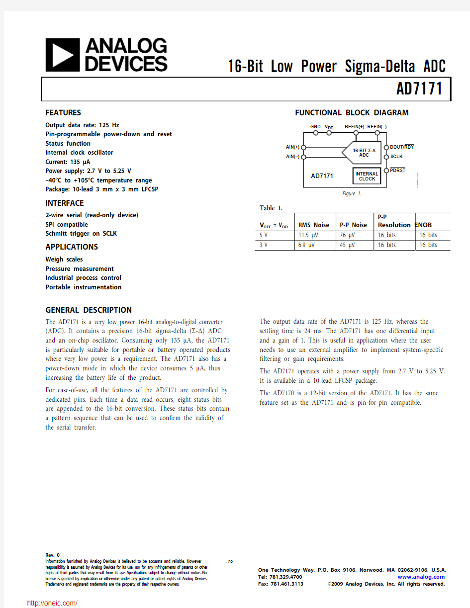
FUNCTIONAL BLOCK DIAGRAM
8
4
1
7
-
1
Figure 1.
Table 1.
V REF = V DD RMS Noise P-P Noise
P-P
Resolution ENOB 5 V 11.5 μV 76 μV 16 bits 16 bits 3 V 6.9 μV 45 μV 16 bits 16 bits
GENERAL DESCRIPTION
The AD7171 is a very low power 16-bit analog-to-digital converter (ADC). It contains a precision 16-bit sigma-delta (Σ-Δ) ADC and an on-chip oscillator. Consuming only 135 μA, the AD7171 is particularly suitable for portable or battery operated products where very low power is a requirement. The AD7171 also has a power-down mode in which the device consumes 5 μA, thus increasing the battery life of the product.
For ease-of-use, all the features of the AD7171 are controlled by dedicated pins. Each time a data read occurs, eight status bits are appended to the 16-bit conversion. These status bits contain a pattern sequence that can be used to confirm the validity of the serial transfer. The output data rate of the AD7171 is 125 Hz, whereas the settling time is 24 ms. The AD7171 has one differential input and a gain of 1. This is useful in applications where the user needs to use an external amplifier to implement system-specific filtering or gain requirements.
The AD7171 operates with a power supply from 2.7 V to 5.25 V. It is available in a 10-lead LFCSP package.
The AD7170 is a 12-bit version of the AD7171. It has the same feature set as the AD7171 and is pin-for-pin compatible.
AD7171
Rev. 0 | Page 2 of 16
TABLE OF CONTENTS
Features .............................................................................................. 1 Interface ............................................................................................. 1 Applications ....................................................................................... 1 Functional Block Diagram .............................................................. 1 General Description ......................................................................... 1 Revision History ............................................................................... 2 Specifications ..................................................................................... 3 Timing Characteristics ..................................................................... 5 Timing Diagrams .......................................................................... 5 Absolute Maximum Ratings ............................................................ 6 Thermal Resistance ...................................................................... 6 ESD Caution .................................................................................. 6 Pin Configuration and Function Descriptions ............................. 7 Typical Performance Characteristics ............................................. 8 Output Noise and Resolution Specifications ................................ 9 ADC Circuit Information .............................................................. 10 Overview ..................................................................................... 10 Filter, Data Rate, and Settling Time ......................................... 10 Gain .............................................................................................. 10 Power-Down/Reset(PDRST ) .................................................... 10 Analog Input Channel ............................................................... 10 Bipolar Configuration ................................................................ 10 Data Output Coding .................................................................. 11 Reference ..................................................................................... 11 Digital Interface .......................................................................... 11 Grounding and Layout .............................................................. 12 Applications Information .............................................................. 13 Temperature System ................................................................... 13 S S ignal C onditioning C ircuit ........................................................ 13 Outline Dimensions ....................................................................... 14 Ordering Guide .. (14)
REVISION HISTORY
10/09—Revision 0: Initial Version
AD7171
SPECIFICATIONS
V DD = 2.7 V to 5.25 V, V REF = V DD, GND = 0 V, all specifications T MIN to T MAX, unless otherwise noted.
Rev. 0 | Page 3 of 16
AD7171
1 Temperature range is –40°C to +105°C.
2 Specification is not production tested but is supported by characterization data at initial product release.
3 Digital inputs equal to V DD or GND.
Rev. 0 | Page 4 of 16
AD7171
Rev. 0 | Page 5 of 16
TIMING CHARACTERISTICS
V DD = 2.7 V to 5.25 V ,, GND = 0 V , Input Logic 0 = 0 V , Input Logic 1 = V DD , unless otherwise noted.
1 Sample tested during initial release to ensure compliance. All input signals are specified with t R = t F = 5 ns (10% to 90% of V DD ) and timed from a voltage level of 1.6 V. 2
See Figure 3. 3
These numbers are measured with the load circuit shown in Figure 2 and defined as the time required for the output to cross the V OL or V OH limits. 4
SCLK active edge is the falling edge of SCLK.
DD = 5V,DD = 3V)
DD = 5V,DD = 3V)
1.6V
08417-002
Figure 2. Load Circuit for Timing Characterization
TIMING DIAGRAMS
DOUT/RDY (O)I = INPUT, O = OUTPUT
08417-003
Figure 3. Read Cycle Timing Diagram
I = INPUT, O = OUTPUT
08417-004
Figure 4. Resetting the AD7171
AD7171
Rev. 0 | Page 6 of 16
ABSOLUTE MAXIMUM RATINGS
T A = 25°C, unless otherwise noted. Table 3.
Parameter Rating V DD to GND ?0.3 V to +7 V Analog Input Voltage to GND ?0.3 V to V DD + 0.3 V Reference Input Voltage to GND ?0.3 V to V DD + 0.3 V Digital Input Voltage to GND ?0.3 V to V DD + 0.3 V Digital Output Voltage to GND ?0.3 V to V DD + 0.3 V
V INx /Digital Input Current 10 mA Operating Temperature Range ?40°C to +105°C Storage Temperature Range ?65°C to +150°C Maximum Junction Temperature 150°C Lead Temperature, Soldering Reflow 260°C Stresses above those listed under Absolute Maximum Ratings may cause permanent damage to the device. This is a stress rating only; functional operation of the device at these or any other conditions above those indicated in the operational
section of this specification is not implied. Exposure to absolute maximum rating conditions for extended periods may affect device reliability. THERMAL RESISTANCE
θJA is specified for the worst-case conditions, that is, a device soldered in a circuit board for surface-mount packages.
Table 4. Package Type θJA θJC Unit L FCSP 48.7 2.96 °C/W ESD CAUTION
AD7171
Rev. 0 | Page 7 of 16
PIN CONFIGURATION AND FUNCTION DESCRIPTIONS
1SCLK 2DOUT/RDY
3AIN(+)4AIN(–)5
REFIN(+)
10NC
NOTES
1. NC = NO CONNECT.
2. CONNECT EXPOSED PAD TO GROUND.
9PDRST 8V DD 7GND 6
REFIN(–)
AD7171
TOP VIEW (Not to Scale)
08417-005
Figure 5. Pin Configuration
AD7171
Rev. 0 | Page 8 of 16
TYPICAL PERFORMANCE CHARACTERISTICS
10
8
6
420–40–10205080110R M S N O I S E (μV )
TEMPERATURE (°C)08417-015
Figure 6. AD7171 RMS Noise vs. Temperature
0.266–0.200
–0.133–0.0660
0.066
0.133
0.200
–3
3210–1–2I N L (L S B )
V IN
(V)
08417-006
Figure 7. Integral Nonlinearity (V REF = V DD )
180
120140
160
–40
–10205080110
O F F S E T (μV )
TEMPERATURE (°C)08417-007
Figure 8. Offset vs. Temperature 0.025
0.015
0.017
0.021
0.019
0.023
–40
–10205080110
G A I N E R R O R (%)
TEMPERATURE (°C)
08417-008
Figure 9. Gain Error vs. Temperature
140
132
124
116
108
100–40
–10205080110
I D D (μA )
TEMPERATURE (°C)
08417-016
Figure 10. Power Supply Current vs. Temperature
4.54.03.5
3.0
2.52.01.51.00.5
0–40
–10205080110
I D D (μA )
TEMPERATURE (°C)
08417-017Figure 11. Power-Down Current vs. Temperature
AD7171
Rev. 0 | Page 9 of 16
OUTPUT NOISE AND RESOLUTION SPECIFICATIONS
Table 6 shows the rms noise of the AD7171. The numbers given
are for a 5 V and a 3 V reference. These numbers are typical and are generated with a differential input voltage of 0 V . The corres-ponding p-p resolution is also listed along with the effective resolution (ENOB). It is important to note that the effective resolution is calculated using the rms noise, whereas the p-p resolution is based on the p-p noise. The p-p resolution represents the resolution for which there is no code flicker. These numbers are typical.
The effective number of bits (ENOB) is defined as
ENOB = ln (FSR /RMS noise )/ln (2)
The noise-free bits, or p-p resolution, are defined as
Noise -Free Bits = ln (FSR /Peak -to -Peak Noise )/ln (2) where FSR is the full-scale range and is equal to 2 × V REF /gain. Table 6. RMS Noise and Resolution of the AD7171
V REF = V DD RMS Noise P-P Noise P-P
Resolution ENOB 5 V 11.5 μV 76 μV 16 bits 16 bits 3 V
6.9 μV
45 μV
16 bits 16 bits
AD7171
Rev. 0 | Page 10 of 16
750
ADC CIRCUIT INFORMATION
OVERVIEW
The AD7171 is a low power ADC that incorporates a precision 16-bit Σ-Δ modulator and an on-chip digital filter intended for measuring wide dynamic range, low frequency signals. The device has an internal clock and one differential input. It
operates with an output data rate of 125 Hz and has a gain of 1. A 2-wire interface simplifies data retrieval from the AD7171.
FILTER, DATA RATE, AND SETTLING TIME
The AD7171 uses a sinc 3 filter. The output data rate is set to 125 Hz; thus, valid conversions are available every 1/125 = 8 ms. If a reset occurs, then the user must allow the complete settling time for the first conversion after the reset. The settling time is equal to 24 ms. Subsequent conversions are available at 125 Hz. When a step change occurs on the analog input, the AD7171 requires several conversion cycles to generate a valid conversion. If the step change occurs synchronous to the conversion period, then the settling time of the AD7171 must be allowed to generate a valid conversion. If the step change occurs asynchronous to the end of a conversion, then an extra conversion must be allowed to generate a valid conversion. The data register is updated with all the conversions but, for an accurate result, the user must allow the required time.
Figure 12 shows the filter response of the filter. The only external filtering required on the analog inputs is a simple R-C filter to provide rejection at multiples of the master clock. A 1 KΩ resistor in series with each analog input, a 0.01 μF capacitor from each input to GND, and a 0.1 μF capacitor from AIN(+) to AIN(?) are recommended.
0–100
–90
–80–70–60–50–40–30–20–100
625
500
375
250
125
F I L T E R
G A I N (d B )
INPUT SIGNAL FREQUENCY (Hz)
08417-011
Figure 12. Filter Response
GAIN
The AD7171 has a gain of 1. The acceptable analog input range is +V REF . Therefore, with V REF = 5 V , the input range is +5 V .
POWER-DOWN/RESET(PDRST)
The PDRST pin functions as a power-down pin and a reset pin. When PDRST is taken low, the AD7171 is powered down. The entire ADC is powered down (including the on-chip clock), and the DOUT/RDY pin is tristated. The circuitry and serial interface are also reset. This resets the logic, the digital filter, and the analog modulator. PDRST must be held low for 100 ns minimum to initiate the reset function (see ).
Figure 4When PDRST is taken high, the AD7171 is taken out of power-down mode. When the on-chip clock has powered up (1 ms, typically), the modulator then begins sampling the analog input. The DOUT/RDY pin becomes active, going high until a valid conversion is available. A reset is automatically performed on power-up.
ANALOG INPUT CHANNEL
The AD7171 has one differential analog input channel that is connected to the modulator; that is, the input is unbuffered. Note that this unbuffered input path provides a dynamic load to the driving source. Therefore, resistor/capacitor combinations on the input pins can cause dc gain errors, depending on the output impedance of the source that is driving the ADC input. Table 7 shows the allowable external resistance/capacitance values such that no gain error at the 16-bit level is introduced. Table 7. External R-C Combination for No Gain Error
C (pF) R (Ω) 50 9 k 100 6 k 500 1.5 k 1000 900 5000
200
The absolute input voltage range is restricted to a range between GND ? 30 mV and V DD + 30 mV . Care must be taken in setting up the common-mode voltage to avoid exceeding these limits. Otherwise, there is degradation in linearity and noise performance.
BIPOLAR CONFIGURATION
The AD7171 accepts a bipolar input range. A bipolar input range does not imply that the part can tolerate negative voltages with respect to system GND. Signals on the AIN(+) input are referenced to the voltage on the AIN(?) input. For example, if AIN(?) is 2.5 V , the analog input range on the AIN(+) input is 0 V to 5 V when a 2.5 V reference is used.
分销商库存信息:
ANALOG-DEVICES
AD7171BCPZ-500RL7AD7171BCPZ-REEL7EVAL-AD7171EBZ