
Near-ultraviolet photodetector based on hybrid polymer/zinc oxide nanorods by low-temperature solution processes
Yun-Yue Lin,1Chun-Wei Chen,1,a ?Wei-Che Yen,1Wei-Fang Su,1Chen-Hao Ku,2and Jih-Jen Wu 2
1Department of Materials Science and Engineering,National Taiwan University,Taipei 106,Taiwan 2
Department of Chemical Engineering,National Cheng Kung University,Tainan 701,Taiwan
?Received 2April 2008;accepted 15May 2008;published online 10June 2008?
In this article,we have proposed a nanostructured near-ultraviolet photodetector ??400nm ?based on the ZnO nanorod/poly?uorene hybrid by solution processes at low temperature.The current-voltage characteristic of the hybrid device demonstrates the typical pn -heterojunction diode behavior,consisting of p -type polymer and n -type ZnO nanorods,respectively.The relative quantum ef?ciencies of the hybrid device exhibit a nearly three order difference while illuminated under UV and visible light,respectively.The responsivity for the device can reach to 0.18A /W at 300nm by applying a bias of ?2V,which provides a route to fabricate a low-cost near-UV photodetector.?2008American Institute of Physics .?DOI:10.1063/1.2940594?
Due to its direct band gap of 3.37eV and strong exciton binding energy of 60meV,ZnO-based semiconductors are recognized as very promising photonic materials in the ultraviolet ?UV ?region.1–3It has been suggested that semi-conducting nanowires or nanorods may offer additional ad-vantages for optoelectronic device applications due to the increased junction area,enhanced polarization dependence,and improved carrier con?nement in one dimension.Poten-tial applications in many ?elds such as light emitting diodes,4?eld effect transistors,5and dye-sensitizer solar cell 6have also attracted a great attention recently.Another important application for ZnO is the UV detection due to its wide band gap and chemical and thermal stability.Until now,UV detectors based on photoconducting layers 7or metal-semiconductor Schottky barriers 8from ZnO ?lms have been commonly reported.Since p -type doping of ZnO has re-mained a challenge,9as a consequence,UV detectors based on ZnO homojunction or heterojunction structures are still very https://www.doczj.com/doc/392924438.html,pared to most of ZnO nanostructures which are usually prepared in various gas methods in vacuum and high temperature,10,11much lower temperature deposition methods have been developed recently through solution processes.12In this work,we have developed the simple solution processes to fabricate a near-UV ?NUV ?de-tector based on a pn -heterojunction consisting of p -type polymer poly?uorene ?PFO ?and n -type ZnO nanorods.The device can be fabricated by preparing the ZnO nanorods in the much lower deposition temperature regime through solu-tion and utilizing the simple spin-coating method to form the organic/inorganic hybrid thin ?lms.
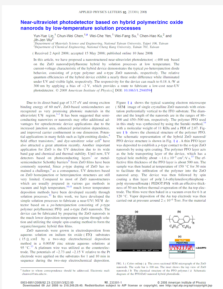
ZnO nanorods were grown in electrodeposition from aqueous solution on indium tin oxide ?ITO ?substrates ?15?/cm 2?by a two-step electrochemical deposition method in a 0.005M zinc nitrate aqueous solutions at 95°C.13A platinum wire was utilized as the counterelec-trode.The potentials of ?2.73and ?2.15V relative to the Pt electrode were applied on the substrates for 1and 10min in sequence during the two-step electrochemical deposition.
Figure 1?a ?shows the typical scanning electron microscope ?SEM ?image of single crystalline ZnO nanorods with orien-tation preferentially vertical to the ITO substrate.The diam-eter and the length of the nanorods are in the ranges of 80–100and 450–500nm,respectively.The polymer PFO used in this study was synthesized by using the Suzuki method,14with a molecular weight of 11KDa and a PDI of 2.07.Fig-ure 1?b ?shows the chemical structure of the polymer PFO.The schematic representation of the hybrid ZnO nanorod/PFO device structure is shown in Fig.1?c ?.A thin PFO layer was deposited to establish a p -type contact to the n -type ZnO nanorods by using spin coating.The polymer PFO layer acts as the hole transporting layer of the device,which has a typical hole mobility about ?1.6?10?5cm 2/V s.15The ef-fective ?lm thickness of the PFO layer is about 500nm.The sample was then heated at temperature of 150°C for 30min to facilitate the in?ltration of the polymer into the ZnO nanorod array.The device was then followed by spin coating a thin layer of poly ?3,4-ethylenedioxythiophene ?-poly ?styrenesulfonate ??PEDOT:PSS ?with an effective thick-ness of 50nm before thermal evaporation of the Au top elec-trode.The ?lms were then baked in a vacuum oven for 6h at 120°C.Vapor deposition of the Au top electrode was then carried out at pressure around 2?10?6Torr.For the material
a ?
Author to whom correspondence should be addressed.Electronic mail:
chunwei@https://www.doczj.com/doc/392924438.html,.tw.
FIG.1.?Color online ??a ?The cross-sectional SEM micrograph of the ZnO nanorods.The scale bar is 100nm.The inset shows the top view of ZnO nanorods.?b ?The chemical structure of the PFO polymer.?c ?Schematic diagram of the PFO/ZnO nanorod hybrid photodiode.
APPLIED PHYSICS LETTERS 92,233301?2008?
0003-6951/2008/92?23?/233301/3/$23.00?2008American Institute of Physics 92,233301-1Downloaded 09 Jul 2008 to 218.249.29.40. Redistribution subject to AIP license or copyright; see https://www.doczj.com/doc/392924438.html,/apl/copyright.jsp
and device characterizations,UV-visible absorption spectra were obtained using an Ocean Optics HR-4000spectrometer.The steady-state photoluminescence ?PL ?spectra were mea-sured by using a Perkin-Elmer FS-55spectro?uorometer.Time-resolved PL ?TRPL ?spectroscopy was performed with a time-correlated single photon counting spectrometer ?Pico-quant,Inc.?.A pulse laser ?375nm ?with an average power of 1mW operating at 40MHz with a duration of 70ps was used for excitation.The ?lm thickness was measured by means of the Veeco M6surface pro?ler.The current-voltage characterizations ?Keithley 2400source meter ?were per-formed under 10?3torr vacuum and under monochromatic illumination at de?ned beam size ?Newport Inc.?.
Figure 2?a ?shows the absorption and PL spectra of the ZnO nanorods and polymer PFO used in this study.For the ZnO nanorods,the fundamental absorption edge is located in the UV region ??375nm ?.The PL spectra exhibit a strong UV emission peak at about 380nm,which is related to the near-band edge emission of the wide band gap ZnO.An ad-ditional green band at ?450–500nm is also observed,which is mainly caused by the intrinsic defects or oxygen vacancies in the ZnO.For the polymer PFO,a broad absorp-tion spectrum ranged from 300–400nm with a peak at about 375nm is observed.Since PFO has an absorption edge about 3eV,it is also almost transparent in the visible region.In addition,the PL spectrum of PFO shows a broad emission range with two distinct vibronic peaks at 423and 448nm,respectively.
Figure 3?a ?shows the current-voltage characteristics of the PFO/ZnO nanorod heterojunction diode measured in the dark and under illumination at 350nm,respectively.The typical p -n junction behavior with the clearly rectifying current-voltage I -V characteristics was obtained in the dark,showing a recti?cation ratio ?current ratio measured at +1versus ?1V ?of 122.This is originated from the formation of p -n junction interfaces between p -typed conjugated polymer and the n -typed ZnO nanorods.Under illumination with a 350nm light source,a typical photovoltaic characteristic curve can be obtained,with a short circuit current density ?J sc ?of 18?A /cm 2,an open circuit voltage ?V oc ?of 335mV,a ?ll factor of 0.46,respectively.The dynamic range of the photodiode at zero bias ?the current ratio be-tween photocurrent and dark current ?is exceeding 104.One of the advantages of operating a photodiode under zero or low bias voltage is the low dark current,low noise level,and large dynamic range.The relative quantum ef?ciencies
?RQEs ?with a spectral range from 300to 700nm for the photodiode based on PFO/ZnO nanorod heterojunctions are shown in Fig.3?b ?,by taking the quantum ef?ciency as 1for the sample under the 300nm illumination.The RQEs of the PFO/ZnO nanorod hybrid device exhibit a nearly three order difference while illuminated under UV ?300nm ?and visible light ?600nm ?,respectively,indicating that the device can be used as a potentially cheap NUV photodetector fabricated from low temperature solution processes.
Figure 4?a ?shows the spectral responsivity S ???of the PFO/ZnO nanorod hybrid photodiode operated at different bias conditions.The number of photogenerated electron-hole pairs at the PFO/ZnO nanorod interface can be further en-hanced by applying a reverse bias to the junction,which may suppress the formation of excitons or decompose excitons into mobile carriers.The responsivity can reach to about 0.18A /W at 300nm for the photodiode operated at ?2V reverse bias.Due to the large overlap in the UV absorption region between PFO and ZnO nanorods,the PFO thin layer can act not only as the hole transport layer but also as the light absorbing layer.The observed signi?cant increase in S ???at the wavelengths between 370and 400nm under ?2V bias may mainly result from the enhanced charge transfer ef?ciency from PFO to ZnO nanorods.The inset in the Fig.4?b ?exhibits the corresponding electronic energy levels for ZnO and PFO obtained from literatures.16,17When the PFO/ZnO nanorod hybrid device is illuminated with a wavelength ?350nm,both PFO and ZnO nanorods can be excited.Photogenerated excitons in ZnO or PFO can be ei-ther recombined radiatively or dissociated from Coulomb at-traction at the interfaces between polymer and ZnO nano-rods,by offering an energetically favorable pathway for the electrons ?holes ?from polymer ?ZnO nanorods ?to transfer onto ZnO nanorods ?polymer ?.When the device is
illumi-
FIG.2.?Color online ?Absorption and PL spectra of ZnO nanorods ?dash line ?and polymer PFO ?solid line ?
respectively.
FIG.3.?Color online ??a ?Current-voltage characteristics of PFO/ZnO na-norod heterojunctions in the dark and under 350nm illumination respec-tively.The incident power is 0.69mW /cm 2.The inset shows the semi-log plot for the above curves.?b ?The RQEs for hybrid device.The quantum ef?ciency under 300nm illumination is taken as 1.
Downloaded 09 Jul 2008 to 218.249.29.40. Redistribution subject to AIP license or copyright; see https://www.doczj.com/doc/392924438.html,/apl/copyright.jsp
nated with a wavelength between 370and 400nm,a large number of excitons are mainly generated from polymer due to the large absorption coef?cient of PFO.Figure 4?b ?shows the TRPL decay spectroscopy for the pristine PFO and PFO/ZnO nanorod hybrid thin ?lms respectively.It is found that the PL lifetime ?hybrid ?380ps ?for the PFO/ZnO nanorod hybrid is much shorter than that of the pristine PFO thin ?lm
?PFO ?875ps ?,suggesting that charge transfer occurs from PFO to ZnO nanorods at the interfaces.This accounts for the signi?cant increase in the photoresponse at the wavelength range between 370and 400nm,resulting from the ef?cient charge transfer from PFO to ZnO nanorods.
In conclusion,we have reported a ZnO nanorod/polymer hybrid NUV photodetector using simple low temperature so-lution processes.We believe this system can be a promising alternative to fabricate the low-cost NUV photodiode since the complete processes are compatible for large area and ?exible substrate fabrications.
This work is supported by National Science Council,Taiwan ?Project Nos.96-2112-M-002-030-MY3and NSC 96-2120-M-001-001?.
1
H.J.Ko,Y .F.Chen,Z.Zhu,T.Yao,I.Kaobayyashi,and H.Uchiki,Appl.Phys.Lett.76,1905?2000?.2
W.I.Park,Y .H.Jun,S.W.Jung,and G.-C.Yi,Appl.Phys.Lett.82,964?2003?.3
M.H.Huang,S.Mao,H.Feick,H.Yan,Y .Wu,H.Kind,E.Weber,R.Russo,and P.Yang,Science 292,1897?2001?.4
A.Tsukazaki,A.Ohtomo,T.Onuma,M.Ohtani,T.Makino,M.Sumiya,K.Ohtani,S.F.Chichibu,S.Fuke,Y .Segawa,H.Ohno,H.Koinuma,and M.Kawasaki,Nat.Mater.4,42?2005?.5
W.I.Park,J.S.Kim,G.-C.Yi,M.H.Bae,and H.-J.Lee,Appl.Phys.Lett.85,5052?2003?.6
https://www.doczj.com/doc/392924438.html,w,L.E.Greene,J.C.Johnson,R.Saykally,and P.Yang,Nat.Mater.4,455?2005?.7
D.Basaka,G.Aminb,B.Mallikb,G.K.Paulc,and S.K.Senc,J.Cryst.Growth 256,73?2003?.8
S.Liang,H.Sheng,Y .Liu,Z.Huo,Y .Lu,and H.Shen,J.Cryst.Growth 225,110?2001?.9
S.Limpijumnong,S.B.Zhang,S.-H.Wei,and C.H.Park,Phys.Rev.Lett.92,155504?2004?.10
J.J.Wu,H.I.Wen,C.H.Tseng,and S.C.Liu,Adv.Funct.Mater.14,806?2004?.11
Z.W.Pan,Z.R.Dai,and Z.L.Wang,Science 291,1947?2001?.12
C.H.Ku and J.-J.Wu,J.Phys.Chem.B 110,12981?2006?.13
J.Cui and U.J.Gibson,J.Phys.Chem.B 109,22074?2005?.14
A.Suzuki and N.Miyaura,Chem.Rev.?Washington,D.C.?95,2457?1995?.15
R.Pacios,J.Nelson,D.C.Bradley,and C.J.Brabec,Appl.Phys.Lett.83,4764?2003?.16
M.Graetzel,Nature ?London ?414,338?2001?.17
G.Greczynskia,Th.Kugler,and W.R.Salaneck,J.Appl.Phys.88,7187?2000?
.
FIG.4.?Color online ??a ?Spectral response of the hybrid photodiode at different biases.The dash line shows the absorption spectra of PFO.?b ?The PL decay curves for the pristine PFO and PFO/ZnO nanorod hybrid thin ?lms,respectively.The exciting wavelength of the pulse is 375nm and the PL emission wavelength is probed at 423nm of PFO The inset shows the corresponding energy levels for the materials used in the device.
Downloaded 09 Jul 2008 to 218.249.29.40. Redistribution subject to AIP license or copyright; see https://www.doczj.com/doc/392924438.html,/apl/copyright.jsp