MAX17006AETP+中文资料
- 格式:pdf
- 大小:316.24 KB
- 文档页数:23
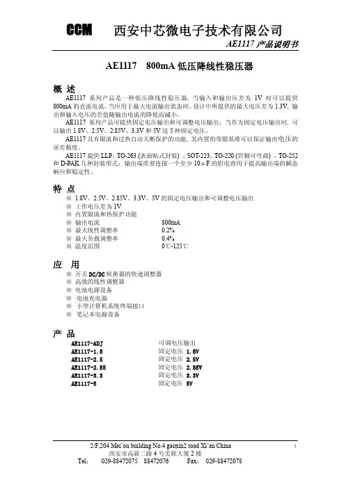
AE1117 800mA低压降线性稳压器概述AE1117系列产品是一种低压降线性稳压器, 当输入和输出压差为1V时可以提供800mA的直流电流,当应用于最大电流输出状态时,设计中所提供的最大电压差为1.3V, 输出和输入电压的差值随输出电流的降低而减小。
AE1117系列产品可提供固定电压输出和可调整电压输出;当作为固定电压输出时, 可以输出1.8V、2.5V、2.85V、3.3V和5V这5种固定电压。
AE1117具有限流和过热自动关断保护的功能, 其内置的带隙基准可以保证输出电压的误差精度。
AE1117提供LLP、TO-263 (表面贴式封装) 、SOT-223、TO-220 (管脚可弯曲) 、TO-252和D-PAK几种封装型式;输出端需要连接一个至少10μF的钽电容用于提高输出端的瞬态响应和稳定性。
特点※ 1.8V、2.5V、2.85V、3.3V、5V的固定电压输出和可调整电压输出※ 工作电压差为1V※ 内置限流和热保护功能※ 输出电流800mA※ 最大线性调整率0.2%※ 最大负载调整率0.4%※ 温度范围0℃-125℃应用※ 开关DC/DC转换器的快速调整器※ 高效的线性调整器※ 电池电源设备※ 电池充电器※ 小型计算机系统终端接口※ 笔记本电源设备产品AE1117-ADJ 可调电压输出AE1117-1.8 固定电压 1.8VAE1117-2.5 固定电压 2.5VAE1117-2.85 固定电压 2.85VAE1117-3.3 固定电压 3.3VAE1117-5 固定电压 5V2/F,204 Mei’ou building No.4 gaoxin2 road Xi’an China 12/F,204 Mei’ou building No.4 gaoxin2 road Xi’an China2功能框图管脚图2/F,204 Mei’ou building No.4 gaoxin2 road Xi’an China3管脚说明V IN AE1117的电压输入端,各个电压档次的产品可以根据不同输入要求在最小值和最大值之间变化。
MAX4616ESD中文资料19-1501;Rev0;7/99Low-Voltage,High-Speed,Quad,SPSTCMOSAnalogSwitche____________________________FeatureTheMA某4614/MA某4615/MA某4616quad,low-voltage,oFatSwitchingTimeEachwitchhandleV+toGNDanalogignallevel.Ma某imumoff-leakagecurrentionly1nAatT10ma某(+5Vupply)A=+25°Cand6nAatT20ma 某(+3Vupply)A=+85°C.________________________ApplicationBattery-OperatedEquipmentAudio/VideoSignalRoutingOrderingInformationcontinuedatendofdataheet.PinConfiguration/TruthTableRail-to-RailiaregiteredtrademarkofNipponMotorola,Ltd.____________________________________________________________ ____Ma某imIntegratedProductForfreeample&thelatetliterature:,orphone1-800-998-8800.Formallorder,phone1-800-835-8769.MA某4614/MA某4615/MA某4616Low-Voltage,High-Speed,Quad,SPSTCMOSAnalogSwitcheMA某4614/MA某4615/MA某4616ABSOLUTEMA某IMUMRATINGS(VoltagereferencedtoGND)V+,IN_...................................................... ................-0.3Vto+6VCOM_,NO_,NC_(Note1).........................-0.3Vto(V++0.03V)ContinuouCurrent(anyterminal)................... .................±75mAPeakCurrent(NO_,NC_,COM_)(puledat1m,10%dutycycle).................................±2 00mAContinuouPowerDiipation(TA=+70°C)14-PinTSSOP(derate6.3mW/°Cabove+70°C)..........500mW14-PinNarrowSO(derate8.00mW/°Cabove+70°C)..640mW14-PinPlaticDIP(derate10.00mW/°Cabove+70°C)...800mWOperatingTempe ratureRangeMA某461_C__......................................................0°Cto+70°CMA某461_E__....................................................-40°Cto+85°CStorageTemperatureRange............................ .-65°Cto+150°CLeadTemperature(oldering,10ec).................... .........+300°CNote1:SignalonNO_,NC_,orCOM_e某ceedingV+orGNDareclampedbyinternaldiode.Limitforward-diodecurrenttoma某i-mumcurrentrating.Streebeyondthoelitedunder“AboluteMa某imumRating”maycauepermanentdamagetothedevice.Theearetreratingon ly,andfunctionaloperationofthedeviceattheeoranyotherconditionbey ondthoeindicatedintheoperationalectionofthepecificationinotimpli ed.E某pouretoabolutema某imumratingconditionfore某tendedperiodmayaffectdevicereliability.ELECTRICALCHARACTERISTICS—Single+5VSupply(V+=+5V±10%,VIN_H=2.4V,VIN_L=0.8V,TA=TMINtoTMA某,unleotherwienoted.)(Note2)2___________________________________________________________ ____________________________Low-Voltage,High-Speed,Quad,SPSTCMOSAnalogSwitcheELECTRICALCHARACTERISTICS—Single+5VSupply(continued)(V+=+5V±10%,VIN_H=2.4V,VIN_L=0.8V,TA=TMINtoTMA某,unleotherwienoted.)(Note2)_______________________________________________________________ ________________________3MA某4614/MA某4615/MA某4616Low-Voltage,High-Speed,Quad,SPSTCMOSAnalogSwitcheMA某4614/MA某4615/MA某4616ELECTRICALCHARACTERISTICS—Single+3.3VSupply(V+=+3.3V±10%,VIN_H=2.4V,VIN_L=0.5V,TA=TMINtoTMA某,unleotherwienoted.)(Note2)4___________________________________________________________ ____________________________Low-Voltage,High-Speed,Quad,SPSTCMOSAnalogSwitcheELECTRICALCHARACTERISTICS—Single+2.5VSupply(V+=+2.5V,VINH=0.7VCC,VINL=0.5V,TA=TMINtoTMA某,unleotherwienoted.)(Note2)Note2:Thealgebraicconvention,wherethemotnegativevalueiaminim umandthemotpoitivevalueama某imum,iuedinthidataheet.Note3:Guaranteedbydeign.Note4:RON=RON(ma某)-RON(min).Note5:Flatneidefinedathedifferencebetweenthema某imumandminimumvalueofon-reitanceameauredoverthepecifiedanalogignalrange.Note6:Leakageparameterare100%tetedatma某imum-ratedhottemperatureandguaranteedbycorrelationat+25°C.Note7:Off-Iolation=20log10(VCOM_/VNO_),VCOM_=output,VNO_=inputtooffwitch.N ote8:Betweenanytwowitche._______________________________________________________________ ________________________5MA某4614/MA某4615/MA某4616Low-Voltage,High-Speed,Quad,SPSTCMOSAnalogSwitcheMA某4614/MA某4615/MA某4616__________________________________________TypicalOperatingCh aracteritic(V+=+5V,GND=0,TA=+25°C,unleotherwienoted.)ON-RESISTANCEv.VCOM_ANDTEMPERATUREOFF-LEAKAGEv.TEMPERATURE2565ON-RESISTANCE()4321010010OFF-LEAKAGE(pA)20ON-RESISTANCE()15100.10.015000.51.01.52.02.53.03.54.04.55.0VCOM_(V)00.51.01.52.02.53.03.54.04.55.0VCOM_(V)0.001-40-2020406080100TEMPERATURE(°C)ON-LEAKAGEv.TEMPERATURESUPPLYCURRENTv.TEMPERATUREMA某4614-16toc05CHARGEINJECTIONv.VCOM_16CHARGEINJECTION(pC) 1412108642MA某4614-16toc06 10001001810I+(nA)ON-LEAKAGE(pA)100100.11-40-2020406080100TEMPERATURE(°C)0.01-40-2020406080100TEMPERATURE(°C)00.51.01.52.02.53.03.54.04.55.0VCOM_(V)VIN_HINPUTLOGICHIGHTHRESHOLDv.V+ MA某4614-16toc070-10-20GAIN(dB)-30-40-50-60-70-80-9010k100k1M10M100M1.81018014410872360-36-72PHASE(degree)1.6VIN_H(V)1.41.2500M1.02.02.53.03.5V+(V)4.04.55.0-100FREQUENCY(Hz)6___________________________________________________________ ____________________________Low-Voltage,High-Speed,Quad,SPSTCMOSAnalogSwitche____________________________TypicalOperatingCharacteritic(co ntinued)(V+=+5V,GND=0,TA=+25°C,unleotherwienoted.)TOTALHARMONICDISTORTIONPLUSNOISEv.FREQUENCYSWITCHINGTIMEv.VOLTAGE0.05090.04580.040)70.035n()S6%E(0.030MNIT5+G0.025DNHIHT0.0204CTI0.015WS30.01020.005 004k8k12k16k20k022.533.544.555.5FREQUENCY(Hz)V+(V)PinDecription_______________________________________________________________ ________________________7MA某4614/MA某4615/MA某4616Low-Voltage,High-Speed,Quad,SPSTCMOSAnalogSwitcheMA某4614/MA某4615/MA某4616ApplicationInformationPower-SupplySequencingandOvervoltageProtectionDonote某ceedtheabolutema某imumratingbecauetreebeyondthelitedratingmaycaueperma-nentdamagetothedevice.Figure1.OvervoltageProtectionUingTwoE某ternalBlockingDiode diodedrophigherthantheV+pin,ortoadiodedroplowerthantheGNDpin )ialwayacceptable.ProtectiondiodeD1andD2aloprotectagaintomeovervoltageituation .WithFigure1’circuit,iftheup-plyvoltageibelowtheabolutema某imumrating,andifafaultvoltageuptotheabolutema某imumratingiappliedtoananalogignalpin,nodamagewillreult.______________________________________________TetCircuit/Tim ingDiagramFigure2.SwitchingTime8____________________________________________________________ ___________________________Low-Voltage,High-Speed,Quad,SPSTCMOSAnalogSwitcheFigure3.ChargeInjectionFigure4.Off-Iolation/On-ChannelBandwidthFigure5.Crotalk_______________________________________________________________ ________________________9MA某4614/MA某4615/MA某4616Low-Voltage,High-Speed,Quad,SPSTCMOSAnalogSwitcheMA某4614/MA某4615/MA某4616TetCircuit/TimingDiagramTRANSISTORCOUNT:89Figure6.ChannelOff/On-Capacitance10__________________________________________________________ ____________________________Low-Voltage,High-Speed,Quad,SPSTCMOSAnalogSwitche_______________________________________________________________ _______________________11MA某4614/MA某4615/MA某4616Low-Voltage,High-Speed,Quad,SPSTCMOSAnalogSwitcheMA某4614/MA某4615/MA某4616PackageInformation(continued)12____________________Ma某imIntegratedProduct,120SanGabrielDrive,Sunnyvale,CA94086408-737-7600©1999Ma某imIntegratedProductPrintedUSAiaregiteredtrademarkofMa某imIntegratedProduct.。
General DescriptionThe MAX3205E/MAX3207E/MAX3208E low-capaci-tance, ±15kV ESD-protection diode arrays with an inte-grated transient voltage suppressor (TVS) clamp are suitable for high-speed and general-signal ESD protec-tion. Low input capacitance makes these devices ideal for ESD protection of signals in H DTV, PC monitors (DVI™, HDMI™), PC peripherals (FireWire ®, USB 2.0),server interconnect (PCI Express™, Infiniband ®), datacom, and interchassis interconnect. Each channel consists of a pair of diodes that steer ESD current puls-es to V CC or GND.The MAX3205E/MAX3207E/MAX3208E protect against ESD pulses up to ±15kV H uman Body Model, ±8kV Contact Discharge, and ±15kV Air-Gap Discharge, as specified in IEC 61000-4-2. An integrated TVS ensures that the voltage rise seen on V CC during an ESD event is clamped to a known voltage. These devices have a 2pF input capacitance per channel, and a channel-to-channel capacitance variation of only 0.05pF, making them ideal for use on high-speed, single-ended, or dif-ferential signals.The MAX3207E is a two-channel device suitable for USB 1.1, USB 2.0 (480Mbps), and USB OTG applica-tions. The MAX3208E is a four-channel device for Ethernet and FireWire applications. The MAX3205E is a six-channel device for cell phone connectors and SVGA video connections.The MAX3205E is available in 9-bump, tiny chip-scale (UCSP™), and 16-pin, 3mm x 3mm, thin QFN pack-ages. The MAX3207E is available in a small 6-pin SOT23 package. The MAX3208E is available in 10-pin µMAX ®and 16-pin, 3mm x 3mm TQFN packages. All devices are specified for the -40°C to +125°C automo-tive operating temperature range.ApplicationsDVI Input/Output Protection Set-Top Boxes PDAs/Cell Phones Graphics Controller Cards Displays/ProjectorsHigh-Speed, Full-Speed and Low-Speed USB Port ProtectionFireWire IEEE 1394 Ports Consumer EquipmentHigh-Speed Differential Signal ProtectionFeatures♦Low Input Capacitance of 2pF Typical♦Low Channel-to-Channel Variation of 0.05pF from I/O to I/O♦High-Speed Differential or Single-Ended ESD Protection±15kV–Human Body Model±8kV–IEC 61000-4-2, Contact Discharge ±15kV–IEC 61000-4-2, Air-Gap Discharge ♦Integrated Transient Voltage Suppressor (TVS)♦Optimized Pinout for Minimized Stub Instances on Controlled-Impedance Differential-Transmission Line Routing♦-40°C to +125°C Automotive Operating Temperature Range♦UCSP Packaging AvailableMAX3205E/MAX3207E/MAX3208EDual, Quad, and Hex High-Speed Differential ESD-Protection ICsOrdering Information19-3361; Rev 2; 3/05For pricing, delivery, and ordering information,please contact Maxim/Dallas Direct!at 1-888-629-4642, or visit Maxim’s website at .*EP = Exposed pad.FireWire is a registered trademark of Apple Computer, Inc.PCI Express is a trademark of PCI-SIG Corporation.DVI is a trademark of Digital Display Working Group.HDMI is a trademark of HDMI Licensing, LCC.InfiniBand is a registered trademark of InfiniBand Trade Association.UCSP is a trademark and µMAX is a registered trademark of Maxim Integrated Products, Inc.Typical Operating Circuit and Pin Configurations appear at end of data sheet.M A X 3205E /M A X 3207E /M A X 3208EDual, Quad, and Hex High-Speed Differential ESD-Protection ICs 2_______________________________________________________________________________________ABSOLUTE MAXIMUM RATINGSELECTRICAL CHARACTERISTICSStresses beyond those listed under “Absolute Maximum Ratings” may cause permanent damage to the device. These are stress ratings only, and functional operation of the device at these or any other conditions beyond those indicated in the operational sections of the specifications is not implied. Exposure to absolute maximum rating conditions for extended periods may affect device reliability.Note 3:Guaranteed by design, not production tested.V CC to GND...........................................................-0.3V to +6.0V I/O_ to GND................................................-0.3V to (V CC + 0.3V)Continuous Power Dissipation (T A = +70°C)6-Pin SOT23 (derate 8.7mW/°C above +70°C)............696mW 9-Pin UCSP (derate 4.7mW/°C above +70°C).............379mW 10-Pin µMAX (derate 5.6mW/°C above +70°C)...........444mW 16-Pin Thin QFN (derate 20.8mW/°C above +70°C).1667mWOperating Temperature Range .........................-40°C to +125°C Storage Temperature Range.............................-65°C to +150°C Junction Temperature .....................................................+150°C Lead Temperature (soldering, 10s).................................+300°C Bump Temperature (soldering)Infrared (15s)...............................................................+220°C Vapor Phase (60s).......................................................+215°CMAX3205E/MAX3207E/MAX3208EDual, Quad, and Hex High-Speed Differential ESD-Protection ICs_______________________________________________________________________________________3CLAMP VOLTAGE vs. DC CURRENTDC CURRENT (mA)C L A M P V O L T A G E (V )130110907050300.50.70.91.11.31.50.310150LEAKAGE CURRENT vs. TEMPERATUREM A X 3205E t o c 02TEMPERATURE (°C)L E K A G E C U R R E N T (p A )804010100100010,0001-40120INPUT CAPACITANCE vs. INPUT VOLTAGEM A X 3205E t o c 03INPUT VOLTAGE (V)I N P U T C A P A C I T A N C E (p F )43211234005Typical Operating Characteristics(V CC = +5V, T A = +25°C, unless otherwise noted.)M A X 3205E /M A X 3207E /M A X 3208EDetailed DescriptionThe MAX3205E/MAX3207E/MAX3208E low-capacitance,±15kV ESD-protection diode arrays with an integrated transient voltage suppressor (TVS) clamp are suitable for high-speed and general-signal ESD protection. Low input capacitance makes these devices ideal for ESD protection of signals in HDTV, PC monitors (DVI, HDMI),PC peripherals (FireWire, USB 2.0), Server Interconnect (PCI Express, Infiniband), Datacom, and Inter-Chassis Interconnect. Each channel consists of a pair of diodes that steer ESD current pulses to V CC or GND. The MAX3205E, MAX3207E, and MAX3208E are two, four,and six channels (see the Functional Diagram ).The MAX3205E/MAX3207E/MAX3208E are designed to work in conjunction with a device’s intrinsic ESD pro-tection. The MAX3205E/MAX3207E/MAX3208E limit theexcursion of the ESD event to below ±25V peak voltage when subjected to the H uman Body Model waveform.When subjected to the IEC 61000-4-2 waveform, the peak voltage is limited to ±60V when subjected to Contact Discharge. The peak voltage is limited to ±100V when subjected to Air-Gap Discharge. The device protected by the MAX3205E/MAX3207E/MAX3208E must be able to withstand these peak volt-ages, plus any additional voltage generated by the par-asitic of the board.A TVS is integrated into the MAX3205E/MAX3207E/MAX3208E to help clamp ESD to a known voltage. This helps reduce the effects of parasitic inductance on the V CC rail by clamping V CC to a known voltage during an ESD event. For the lowest possible clamp voltage dur-ing an ESD event, placing a 0.1µF capacitor as close to V CC as possible is recommended.Dual, Quad, and Hex High-Speed Differential ESD-Protection ICs 4_______________________________________________________________________________________Functional DiagramApplications InformationDesign ConsiderationsMaximum protection against ESD damage results from proper board layout (see the Layout Recommendations section). A good layout reduces the parasitic series inductance on the ground line, supply line, and protect-ed signal lines. The MAX3205E/MAX3207E/MAX3208E ESD diodes clamp the voltage on the protected lines during an ESD event and shunt the current to GND or V CC . In an ideal circuit, the clamping voltage (V C ) is defined as the forward voltage drop (V F ) of the protec-tion diode, plus any supply voltage present on the cath-ode.For positive ESD pulses:V C = V CC + V F For negative ESD pulses:V C =-V FThe effect of the parasitic series inductance on the lines must also be considered (Figure 1).For positive ESD pulses:For negative ESD pulses:where, I ESD is the ESD current pulse.During an ESD event, the current pulse rises from zeroto peak value in nanoseconds (Figure 2). For example,in a 15kV IEC-61000 Air-Gap Discharge ESD event, the pulse current rises to approximately 45A in 1ns (di/dt =45 x 109). An inductance of only 10nH adds an addi-tional 450V to the clamp voltage, and represents approximately 0.5in of board trace. Regardless of the device’s specified diode clamp voltage, a poor layout with parasitic inductance significantly increases the effective clamp voltage at the protected signal line.Minimize the effects of parasitic inductance by placing the MAX3205E/MAX3207E/MAX3208E as close to the connector (or ESD contact point) as possible.A low-ESR 0.1µF capacitor is recommended between V CC and GND in order to get the maximum ESD protec-tion possible. This bypass capacitor absorbs the charge transferred by a positive ESD event. Ideally, the supply rail (V CC ) would absorb the charge caused by a positive ESD strike without changing its regulated value. All power supplies have an effective output impedance on their positive rails. If a power supply’s effective output impedance is 1Ω, then by using V = I x R, the clamping voltage of V C increases by the equa-tion V C = I ESD x R OUT . A +8kV IEC 61000-4-2 ESD event generates a current spike of 24A. The clamping voltage increases by V C = 24A x 1Ω, or V C = 24V.Again, a poor layout without proper bypassing increas-es the clamping voltage. A ceramic chip capacitor mounted as close as possible to the MAX3205E/MAX3207E/MAX3208E V CC pin is the best choice for this application. A bypass capacitor should also beplaced as close to the protected device as possible.MAX3205E/MAX3207E/MAX3208EDual, Quad, and Hex High-Speed Differential ESD-Protection ICs_______________________________________________________________________________________5Figure 1. Parasitic Series InductanceFigure 2. IEC 61000-4-2 ESD Generator Current WaveformM A X 3205E /M A X 3207E /M A X 3208E±15kV ESD ProtectionESD protection can be tested in various ways. The MAX3205E/MAX3207E/MAX3208E are characterized for protection to the following limits:•±15kV using the Human Body Model•±8kV using the Contact Discharge Method specified in IEC 61000-4-2•±15kV using the IEC 61000-4-2 Air-Gap Discharge MethodESD Test ConditionsESD performance depends on a number of conditions.Contact Maxim for a reliability report that documents test setup, methodology, and results.Human Body ModelFigure 3 shows the H uman Body Model, and Figure 4shows the current waveform it generates when dis-charged into a low impedance. This model consists of a 100pF capacitor charged to the ESD voltage of inter-est, which is then discharged into the device through a 1.5k Ωresistor.IEC 61000-4-2The IEC 61000-4-2 standard covers ESD testing and performance of finished equipment. The MAX3205E/MAX3207E/MAX3208E help users design equipment that meets Level 4 of IEC 61000-4-2. The main differ-ence between tests done using the Human Body Modeland IEC 61000-4-2 is higher peak current in IEC 61000-4-2. Because series resistance is lower in the IEC 61000-4-2 ESD test model (Figure 5), the ESD-withstand voltage measured to this standard is general-ly lower than that measured using the H uman Body Model. Figure 2 shows the current waveform for the ±8kV, IEC 61000-4-2 Level 4, ESD Contact Discharge test. The Air-Gap Discharge test involves approaching the device with a charged probe. The Contact Discharge method connects the probe to the device before the probe is energized.Dual, Quad, and Hex High-Speed Differential ESD-Protection ICs 6_______________________________________________________________________________________Figure 4. Human Body Model Current WaveformLayout RecommendationsProper circuit-board layout is critical to suppress ESD-induced line transients (See Figure 6). The MAX3205E/MAX3207E/MAX3208E clamp to 100V; however, with improper layout, the voltage spike at the device can be much higher. A lead inductance of 10nH with a 45A current spike results in an additional 450V spike on the protected line. It is essential that the layout of the PC board follows these guidelines:1)Minimize trace length between the connector or input terminal, I/O_, and the protected signal line.2)Use separate planes for power and ground to reduce parasitic inductance and to reduce the impedance to the power rails for shunted ESD current.3)Ensure short low-inductance ESD transient return paths to GND and V CC .4)Minimize conductive power and ground loops.5)Do not place critical signals near the edge of the PC board.6)Bypass V CC to GND with a low-ESR ceramic capaci-tor as close to V CC as possible.7)Bypass the supply of the protected device to GND with a low-ESR ceramic capacitor as close to the supply pin as possible.UCSP Applications InformationFor the latest application details on UCSP construction,dimensions, tape carrier information, printed circuit board techniques, bump-pad layout, and recommend-ed reflow temperature profile, as well as the latest infor-mation on reliability testing results, go to the Maxim website at /ucsp for the Application Note, UCSP—A Wafer-Level Chip-Scale Package .Chip InformationDIODE COUNT:MAX3205E: 7MAX3207E: 3MAX3208E: 5PROCESS: BiCMOSMAX3205E/MAX3207E/MAX3208EDual, Quad, and Hex High-Speed Differential ESD-Protection ICs_______________________________________________________________________________________7Typical Operating CircuitM A X 3205E /M A X 3207E /M A X 3208EDual, Quad, and Hex High-Speed Differential ESD-Protection ICs 8_______________________________________________________________________________________Pin ConfigurationsMAX3205E/MAX3207E/MAX3208EDual, Quad, and Hex High-Speed Differential ESD-Protection ICs_______________________________________________________________________________________9Package Information(The package drawing(s) in this data sheet may not reflect the most current specifications. For the latest package outline information,go to /packages .)M A X 3205E /M A X 3207E /M A X 3208EDual, Quad, and Hex High-Speed Differential ESD-Protection ICs 10______________________________________________________________________________________Package Information (continued)(The package drawing(s) in this data sheet may not reflect the most current specifications. For the latest package outline information,go to /packages .)MAX3205E/MAX3207E/MAX3208EDual, Quad, and Hex High-Speed Differential ESD-Protection ICs______________________________________________________________________________________11Package Information (continued)(The package drawing(s) in this data sheet may not reflect the most current specifications. For the latest package outline information,go to /packages .)M A X 3205E /M A X 3207E /M A X 3208EDual, Quad, and Hex High-Speed Differential ESD-Protection ICs 12______________________________________________________________________________________Package Information (continued)(The package drawing(s) in this data sheet may not reflect the most current specifications. For the latest package outline information,go to /packages .)Dual, Quad, and Hex High-SpeedDifferential ESD-Protection ICs Maxim cannot assume responsibility for use of any circuitry other than circuitry entirely embodied in a Maxim product. No circuit patent licenses areimplied. Maxim reserves the right to change the circuitry and specifications without notice at any time.Maxim Integrated Products, 120 San Gabriel Drive, Sunnyvale, CA 94086 408-737-7600 ____________________13©2005 Maxim Integrated Products Printed USAis a registered trademark of Maxim Integrated Products, Inc. Package Information (continued)(The package drawing(s) in this data sheet may not reflect the most current specifications. For the latest package outline information,go to /packages.)MAX3205E/MAX3207E/MAX3208E。
_______________General DescriptionThe MAX4545/MAX4546/MAX4547 are low-voltage T-switches designed for switching RF and video signals from DC to 300MHz in 50Ωand 75Ωsystems. The MAX4545 contains four normally open single-pole/single-throw (SPST) switches. The MAX4546 contains two dual SPST switches (one normally open, one normally closed.)The MAX4547 contains two single-pole/double-throw (SPDT) switches.Each switch is constructed in a “T” configuration, ensuring excellent high-frequency off isolation and crosstalk of -80dB at 10MHz. They can handle Rail-to-Rail ®analog sig-nals in either direction. On-resistance (20Ωmax) is matched between switches to 1Ωmax and is flat (0.5Ωmax) over the specified signal range, using ±5V supplies.The off leakage current is less than 5nA at +25°C and 50nA at +85°C.These CMOS switches can operate with dual power sup-plies ranging from ±2.7V to ±6V or a single supply between +2.7V and +12V. All digital inputs have 0.8V/2.4V logic thresholds, ensuring both TTL- and CMOS-logic com-patibility when using ±5V or a single +5V supply.________________________ApplicationsRF SwitchingVideo Signal RoutingHigh-Speed Data Acquisition Test Equipment ATE Equipment Networking____________________________Featureso Low 50ΩInsertion Loss: -1dB at 100MHz o High 50ΩOff Isolation: -80dB at 10MHz o Low 50ΩCrosstalk: -80dB at 10MHz o DC to 300MHz -3dB Signal Bandwidth o 20ΩSignal Paths with ±5V Supplies o 1ΩSignal-Path Matching with ±5V Supplies o 0.5ΩSignal-Path Flatness with ±5V Supplies o ±2.7V to ±6V Dual Supplies +2.7V to +12V Single Supply o Low Power Consumption: <1µW o Rail-to-Rail Bidirectional Signal Handling o Pin Compatible with Industry-Standard DG540, DG542, DG643o >2kV ESD Protection per Method 3015.7o TTL/CMOS-Compatible Inputs with Single +5V or ±5VMAX4545/MAX4546/MAX4547Quad/Dual, Low-Voltage,Bidirectional RF/Video Switches________________________________________________________________Maxim Integrated Products1_____________________Pin Configurations/Functional Diagrams/Truth Tables19-1232; Rev 0; 6/97Ordering Information continued at end of data sheet.For free samples & the latest literature: , or phone 1-800-998-8800Rail-to-Rail is a registered trademark of Nippon Motorola Ltd.M A X 4545/M A X 4546/M A X 4547Quad/Dual, Low-Voltage,Bidirectional RF/Video Switches 2_______________________________________________________________________________________ABSOLUTE MAXIMUM RATINGSELECTRICAL CHARACTERISTICS—Dual Supplies(V+ = +4.5V to +5.5V, V- = -4.5V to -5.5V, V INL = 0.8V, V INH = 2.4V, V GND_= 0V, T A = T MIN to T MAX , unless otherwise noted. Typical values are at T A = +25°C.)Stresses beyond those listed under “Absolute Maximum Ratings” may cause permanent damage to the device. These are stress ratings only, and functional operation of the device at these or any other conditions beyond those indicated in the operational sections of the specifications is not implied. Exposure to absolute maximum rating conditions for extended periods may affect device reliability.(Voltages Referenced to GND)V+...........................................................................-0.3V, +13.0V V-............................................................................-13.0V, +0.3V V+ to V-...................................................................-0.3V, +13.0V All Other Pins (Note 1)..........................(V- - 0.3V) to (V+ + 0.3V)Continuous Current into Any Terminal..............................±25mA Peak Current into Any Terminal(pulsed at 1ms, 10% duty cycle)..................................±50mA ESD per Method 3015.7..................................................>2000V Continuous Power Dissipation (T A = +70°C) (Note 2)16-Pin Plastic DIP(derate 10.53mW/°C above +70°C)..........................842mW16-Pin Narrow SO(derate 8.70mW/°C above +70°C)............................696mW 16-Pin QSOP (derate 8.3mW/°C above +70°C)..........667mW 20-Pin Plastic DIP (derate 8.0mW/°C above +70°C)...640mW 20-Pin Wide SO (derate 10.00mW/°C above +70°C)..800mW 20-Pin SSOP (derate 8.0mW/°C above +70°C)..........640mW Operating Temperature RangesMAX454_C_ E.....................................................0°C to +70°C MAX454_E_ E..................................................-40°C to +85°C Storage Temperature Range.............................-65°C to +150°C Lead Temperature (soldering, 10sec).............................+300°CNote 1:Voltages on all other pins exceeding V+ or V- are clamped by internal diodes. Limit forward diode current to maximum cur-rent rating.MAX4545/MAX4546/MAX4547Quad/Dual, Low-Voltage,Bidirectional RF/Video Switches_______________________________________________________________________________________3ELECTRICAL CHARACTERISTICS—Dual Supplies (continued)(V+ = +4.5V to +5.5V, V- = -4.5V to -5.5V, V INL = 0.8V, V INH = 2.4V, V GND_= 0V, T A = T MIN to T MAX , unless otherwise noted. Typical values are at T A = +25°C.)M A X 4545/M A X 4546/M A X 4547Quad/Dual, Low-Voltage,Bidirectional RF/Video Switches 4_______________________________________________________________________________________ELECTRICAL CHARACTERISTICS—Single +5V Supply(V+ = +4.5V to +5.5V, V- = 0V, V INL = 0.8V, V INH = 2.4V, V GND_= 0V, T A = T MIN to T MAX , unless otherwise noted. Typical values are at T A = +25°C.)MAX4545/MAX4546/MAX4547Quad/Dual, Low-Voltage,Bidirectional RF/Video Switches_______________________________________________________________________________________5ELECTRICAL CHARACTERISTICS—Single +3V Supply(V+ = +2.7V to +3.6V, V- = 0V, V INL = 0.8V, V INH = 2.4V, V GND_ = 0V, T A = T MIN to T MAX , unless otherwise noted. Typical values are at T A = +25°C.)Note 2:The algebraic convention is used in this data sheet; the most negative value is shown in the minimum column.Note 3:Guaranteed by design.Note 4:∆R ON = ∆R ON(MAX)- ∆R ON(MIN).Note 5:Resistance flatness is defined as the difference between the maximum and the minimum value of on-resistance as mea-sured over the specified analog signal range.Note 6:Leakage parameters are 100% tested at the maximum rated hot temperature and guaranteed by correlation at +25°C.Note 7:Off isolation = 20log 10[V COM / (V NC or V NO )], V COM = output, V NC or V NO = input to off switch.Note 8:Between any two switches.Note 9:Leakage testing for single-supply operation is guaranteed by testing with dual supplies.M A X 4545/M A X 4546/M A X 4547Quad/Dual, Low-Voltage,Bidirectional RF/Video Switches 6_________________________________________________________________________________________________________________________________Typical Operating Characteristics(V+ = +5V, V- = -5V, T A = +25°C, GND = 0V, packages are surface mount, unless otherwise noted.)10010-51234-4-3-2-15ON-RESISTANCE vs. V COM(DUAL SUPPLIES)V COM (V)R O N (Ω)5111315971723192125-5-3-2-4-1012345ON-RESISTANCE vs. V COM AND TEMPERATURE (DUAL SUPPLIES)V COM (V)R O N (Ω)10001010012345678910ON-RESISTANCE vs. V COM(SINGLE SUPPLY)V COM (V)R O N (Ω)102025153040354501.0 1.50.52.0 2.53.0 3.54.0 4.55.0ON-RESISTANCE vs. V COM AND TEMPERATURE (SINGLE SUPPLY)V COM (V)R O N (Ω)050100150200250±2±3±4±5±6±8ON/OFF TIME vs.SUPPLY VOLTAGEM A X 4545 T O C 07V+, V- (V)t O N , t O F F (n s )t ONt OFF0.00010.0010.010.1110-75-50-25257550100125ON/OFF-LEAKAGE CURRENT vs.TEMPERATURETEMPERATURE (°C)L E A K A G E (n A)-20204006010080120-5-3-2-4-1012345CHARGE INJECTION vs. V COMV COM (V)Q j (p C )103050709011020406080100-75-2575125-502550100ON/OFF TIME vs.TEMPERATUREM A X 4545 T O C 08TEMPERATURE (°C)t O N , t O F F (n s )t ONt OFF0.000010.00010.001I-I+0.010.11-75-2575125-502550100POWER-SUPPLY CURRENT vs. TEMPERATUREM A X 4545 T O C 09TEMPERATURE (°C)I +, I - (µA )MAX4545/MAX4546/MAX4547Quad/Dual, Low-Voltage,Bidirectional RF/Video Switches_______________________________________________________________________________________70.40.20.61.21.41.00.81.601.0 1.52.0 2.50.53.0 3.54.0 4.55.0LOGIC-LEVEL THRESHOLD vs. POSITIVE SUPPLY VOLTAGEM A X 4545 T O C 10V+ (V)L O G I C -L E V E L T H R E S H O L D (V )-1200.11010001001MAX4545FREQUENCY RESPONSE-100-110FREQUENCY (MHz)L O S S (d B )-80-90-60-50-70-40-20-10-30-1001101001000MAX4546FREQUENCY RESPONSE-60-70-80-90-30-40-50-20-10FREQUENCY (MHz)L O S S (d B )100-20-10-1001101000FREQUENCY RESPONSE-70-80-90-30-40-50-601006080-100-40-60-8040200-20FREQUENCY (MHz)S W I T C H L O S S (d B )O N P H A S E (D E G R E E S )1001000.0001101k 100k10k100MAX4547TOTAL HARMONIC DISTORTIONvs. FREQUENCY0.001FREQUENCY (Hz)T H D (%)0.010.1110____________________________Typical Operating Characteristics (continued)(V+ = +5V, V- = -5V, T A = +25°C, GND = 0V, packages are surface mount, unless otherwise noted.)_______________Theory of OperationLogic-Level TranslatorsThe MAX4545/MAX4546/MAX4547 are constructed as high-frequency “T” switches, as shown in Figure 1. The logic-level input, IN_, is translated by amplifier A1 into a V+ to V- logic signal that drives amplifier A2. (Amplifier A2 is an inverter for normally closed switches.)Amplifier A2 drives the gates of N-channel MOSFETs N1 and N2 from V+ to V-, turning them fully on or off.The same signal drives inverter A3 (which drives the P-channel MOSFETs P1 and P2) from V+ to V-, turning them fully on or off, and drives the N-channel MOSFET N3 off and on.The logic-level threshold is determined by V+ and GND_. The voltage on GND_ is usually at ground potential, but it may be set to any voltage between (V+ - 2V) and V-. When the voltage between V+ and GND_ is less than 2V, the level translators become very slow and unreliable. Since individual switches in each package have individual GND_ pins, they may be set to different voltages. Normally, however, they should all be connected to the ground plane.Switch On ConditionWhen the switch is on, MOSFETs N1, N2, P1, and P2are on and MOSFET N3 is off. The signal path is COM_to NO_, and because both N-channel and P-channel MOSFETs act as pure resistances, it is symmetrical(i.e., signals may pass in either direction). The off MOSFET, N3, has no DC conduction, but has a small amount of capacitance to GND_. The four on MOSFETs also have capacitance to ground that,together with the series resistance, forms a lowpass fil-ter. All of these capacitances are distributed evenly along the series resistance, so they act as a transmis-sion line rather than a simple R-C filter. This helps to explain the exceptional 300MHz bandwidth when the switches are on.M A X 4545/M A X 4546/M A X 4547Quad/Dual, Low-Voltage,Bidirectional RF/Video Switches 8_____________________________________________________________________________________________________________________________________________________Pin Description*All pins have ESD diodes to V- and V+.**NO_ (or NC_) and COM_ pins are identical and interchangeable. Either may be considered as an input or output; signals passequally well in either direction.Figure 1. T-Switch ConstructionTypical attenuation in 50Ωsystems is -1dB and is rea-sonably flat up to 100MHz. Higher-impedance circuits show even lower attenuation (and vice versa), but slightly lower bandwidth due to the increased effect of the internal and external capacitance and the switch’s internal resistance.The MAX4545/MAX4546/MAX4547 are optimized for ±5V operation. Using lower supply voltages or a single supply increases switching time, increases on-resis-tance (and therefore on-state attenuation), and increas-es nonlinearity.Switch Off Condition When the switch is off, MOSFETs N1, N2, P1, and P2 are off and MOSFET N3 is on. The signal path is through the off-capacitances of the series MOSFETs, but it is shunted to ground by N3. This forms a high-pass filter whose exact characteristics are dependent on the source and load impedances. In 50Ωsystems, and below 10MHz, the attenuation can exceed 80dB. This value decreases with increasing frequency and increasing circuit impedances. External capacitance and board layout have a major role in determining over-all performance.__________Applications InformationPower-Supply ConsiderationsOverview The MAX4545/MAX4546/MAX4547 construction is typi-cal of most CMOS analog switches. It has three supply pins: V+, V-, and GND. V+ and V- are used to drive the internal CMOS switches and set the limits of the analog voltage on any switch. Reverse ESD protection diodes are internally connected between each analog signal pin and both V+ and V-. If the voltage on any pin exceeds V+ or V-, one of these diodes will conduct. During normal operation these reverse-biased ESD diodes leak, forming the only current drawn from V-. Virtually all the analog leakage current is through the ESD diodes. Although the ESD diodes on a given sig-nal pin are identical, and therefore fairly well balanced, they are reverse biased differently. Each is biased by either V+ or V- and the analog signal. This means their leakages vary as the signal varies. The difference in the two diode leakages from the signal path to the V+ and V- pins constitutes the analog signal-path leakage cur-rent. All analog leakage current flows to the supply ter-minals, not to the other switch terminal. This explains how both sides of a given switch can show leakage currents of either the same or opposite polarity.There is no connection between the analog signal paths and GND. The analog signal paths consist of an N-channel and P-channel MOSFET with their sources and drains paralleled and their gates driven out of phase with V+ and V- by the logic-level translators.V+ and GND power the internal logic and logic-level translators, and set the input logic thresholds. The logic-level translators convert the logic levels to switched V+ and V- signals to drive the gates of the analog switches. This drive signal is the only connec-tion between the logic supplies and the analog sup-plies. All pins have ESD protection to V+ and to V-. Increasing V- has no effect on the logic-level thresh-olds, but it does increase the drive to the P-channel switches, reducing their on-resistance. V- also sets the negative limit of the analog signal voltage.The logic-level thresholds are CMOS and TTL compati-ble when V+ is +5V. As V+ is raised, the threshold increases slightly; when V+ reaches +12V, the level threshold is about 3.1V, which is above the TTL output high-level minimum of 2.8V, but still compatible with CMOS outputs.Bipolar-Supply Operation The MAX4545/MAX4546/MAX4547 operate with bipolar supplies between ±2.7V and ±6V. The V+ and V- sup-plies need not be symmetrical, but their sum cannot exceed the absolute maximum rating of 13.0V. Do not connect the MAX4545/MAX4546/MAX4547 V+ pin to +3V and connect the logic-level input pins to TTL logic-level signals. TTL logic-level outputs can exceed the absolute maximum ratings, causing damage to the part and/or external circuits.CAUTION:The absolute maximum V+ to V- differential voltage is 13.0V. Typical “±6-Volt” or “12-Volt”supplies with ±10% tolerances can be as high as 13.2V. This voltage can damage the MAX4545/MAX4546/MAX4547. Even ±5% toler-ance supplies may have overshoot or noise spikes that exceed 13.0V.Single-Supply Operation The MAX4545/MAX4546/MAX4547 operate from a sin-gle supply between +2.7V and +12V when V- is con-nected to GND. All of the bipolar precautions must be observed. Note, however, that these parts are opti-mized for ±5V operation, and most AC and DC charac-teristics are degraded significantly when departing from ±5V. As the overall supply voltage (V+ to V-) is lowered, switching speed, on-resistance, off isolation, and distortion are degraded. (See Typical Operating Characteristics.) MAX4545/MAX4546/MAX4547Quad/Dual, Low-Voltage,Bidirectional RF/Video Switches _______________________________________________________________________________________9M A X 4545/M A X 4546/M A X 4547Single-supply operation also limits signal levels and interferes with grounded signals. When V- = 0V, AC sig-nals are limited to -0.3V. Voltages below -0.3V can be clipped by the internal ESD-protection diodes, and the parts can be damaged if excessive current flows.Power OffWhen power to the MAX4545/MAX4546/MAX4547 is off (i.e., V+ = 0V and V- = 0V), the Absolute Maximum Ratings still apply. This means that neither logic-level inputs on IN_ nor signals on COM_, NO_, or NC_ can exceed ±0.3V. Voltages beyond ±0.3V cause the inter-nal ESD-protection diodes to conduct, and the parts can be damaged if excessive current flows.GroundingDC Ground ConsiderationsSatisfactory high-frequency operation requires that careful consideration be given to grounding. For most applications, a ground plane is strongly recom-mended, and all GND_ pins should be connected to it with solid copper.While the V+ and V- power-supply pins are common to all switches in a given package,each switch has separate ground pins that are not internally connected to each other. This contributes to the overall high-frequency performance and provides added flexibility in some applications, but it can cause problems if it is overlooked. All the GND_ pins have ESD diodes to V+ and V-.In systems that have separate digital and analog (sig-nal) grounds, connect these switch GND_ pins to ana-log ground. Preserving a good signal ground is much more important than preserving a digital ground.Ground current is only a few nanoamps.The logic-level inputs, IN_, have voltage thresholds determined by V+ and GND_. (V- does not influence the logic-level threshold.) With +5V and 0V applied to V+ and GND_, the threshold is about 1.6V, ensuring compatibility with TTL- and CMOS-logic drivers.The various GND_ pins can be connected to separate voltage potentials if any or all of the logic-level inputs is not a normal logic signal. (The GND_ voltages cannot exceed (V+ - 2V) or V-.) Elevating GND_ reduces off isolation. For example, using the MAX4545, if GND2–GND6 are connected to 0V and GND1 is connected to V-, then switches 2, 3, and 4 would be TTL/CMOS com-patible, but switch 1 (IN1) could be driven with the rail-to-rail output of an op amp operating from V+ and V-.Note, however, that IN_ can be driven more negative than GND_, as far as V-. GND_ does not have to be removed from 0V when IN_ is driven from bipolar sources, but the voltage on IN_ should never exceed V-.GND_ should be separated from 0V only if the logic-level threshold has to be changed.Any GND_ pin not connected to 0V should be bypassed to the ground plane with a surface-mount 10nF capacitor to maintain good RF grounding. DC current in the IN_ and GND_ pins is less than 1nA, but increases with switching frequency.On the MAX4545 only, two extra ground pins—GND5and GND6—are provided to improve isolation and crosstalk. They are not connected to the logic-level cir-cuit. These pins should always be connected to the ground plane with solid copper.AC Ground and BypassingA ground plane is mandatory for satisfactory high-frequency operation.(Prototyping using hand wiring or wire-wrap boards is strongly discouraged.) Connect all 0V GND_ pins to the ground plane with solid copper.(The GND_ pins extend the high-frequency ground through the package wire-frame, into the silicon itself,thus improving isolation.) The ground plane should be solid metal underneath the device, without interruptions.There should be no traces under the device itself. For DIP packages, this applies to both sides of a two-sided board. Failure to observe this will have a minimal effect on the “on” characteristics of the switch at high frequen-cies, but it will degrade the off isolation and crosstalk.All V+ and V- pins should be bypassed to the ground plane with surface-mount 10nF capacitors. For DIP packages, they should be mounted as close as possi-ble to the pins on the same side of the board as the device. Do not use feedthroughs or vias for bypass capacitors. For surface-mount packages, the pins are so close to each other that the bypass capacitors should be mounted on the opposite side of the board from the device. In this case, use short feedthroughs or vias, directly under the V+ and V- pins. Any GND_ pin not connected to 0V should be similarly bypassed. If V-is 0V, connect it directly to the ground plane with solid copper. Keep all leads short.The MAX4547 has two V+ and V- pins. Make DC con-nections to only one of each to minimize crosstalk. Do not route DC current into one of the V+ or V- pins and out the other V+ or V- pin to other devices. The second set of V+ and V- pins is for AC bypassing only.For dual-supply operation, the MAX4547 should have four 10nF bypass capacitors connected to each V+and V- pin, as close to the package as possible. For single-supply operation, the MAX4547 should have two 10nF bypass capacitors connected (one to each V+pin), as close to the package as possible.Quad/Dual, Low-Voltage,Bidirectional RF/Video Switches 10______________________________________________________________________________________MAX4545/MAX4546/MAX4547Bidirectional RF/Video Switches______________________________________________________________________________________11On the MAX4545, GND5 and GND6 should always be connected to the ground plane with solid copper to improve isolation and crosstalk.Signal RoutingKeep all signal leads as short as possible. Separate all signal leads from each other and other traces with the ground plane on both sides of the board. Where possi-ble, use coaxial cable instead of printed circuit board traces.Board LayoutIC sockets degrade high-frequency performance and should not be used if signal bandwidth exceeds 5MHz.Surface-mount parts, having shorter internal lead frames, provide the best high-frequency performance.Keep all bypass capacitors close to the device, and separate all signal leads with ground planes. Such grounds tend to be wedge-shaped as they get closer to the device. Use vias to connect the ground planes on each side of the board, and place the vias in the apex of the wedge-shaped grounds that separate signal leads.Logic-level signal lead placement is not critical.Impedance MatchingThe typical on-resistances of the switches in the MAX4545/MAX4546/MAX4547 are 14Ω, but the off-state impedances are approximately equal to a 6pF capacitor. In coaxial systems, therefore, it is impossible to match any impedance for both the on and off state. If impedance matching is critical, the MAX4546 is best suited, since its two sections can be configured as a single on/off switch, as shown in Figure 2. This circuit “wastes” switches and has higher losses, but has bet-ter off isolation and maintains good impedance match-ing in both the on and off states. The resistance values shown in Figure 3 are optimized with ±5V supplies for both 50Ωand 75Ωsystems at room temperature.MultiplexerWith its excellent off isolation, the MAX4545 is ideal for use in high-frequency video multiplexers. Figure 3shows such an application for switching any one of four video inputs to a single output. The same circuit may be used as a demultiplexer by simply reversing the sig-nal direction.Stray capacitance of traces and the output capacitance of switches placed in parallel reduces bandwidth, so the outputs of no more than four individual switches should be placed in parallel if high bandwidth is to be main-tained. If more than four mux channels are needed, the 4-channel circuit should be duplicated and cascaded.Figure 2. Impedance Matching On/Off SwitchM A X 4545/M A X 4546/M A X 4547Bidirectional RF/Video Switches 12______________________________________________________________________________________Figure 3. 4-Channel MultiplexerMAX4545/MAX4546/MAX4547Bidirectional RF/Video Switches______________________________________________________________________________________13Figure 4. Switching Time______________________________________________Test Circuits/Timing DiagramsFigure 5. Break-Before-Make Interval (MAX4546/MAX4547 only)M A X 4545/M A X 4546/M A X 4547Bidirectional RF/Video Switches 14______________________________________________________________________________________Figure 6. Charge InjectionFigure 7. On Loss, Off Isolation, and Crosstalk_________________________________Test Circuits/Timing Diagrams (continued)MAX4545/MAX4546/MAX4547Bidirectional RF/Video Switches______________________________________________________________________________________15N.C. = NO INTERNAL CONNECTIONTRANSISTOR COUNT: 253SUBSTRATE INTERNALLY CONNECTED TO V-GND2GND5GND4NO4V-NO1COM30.101"(2.565mm)0.085"(2.159mm)COM4IN4IN3GND6V+NO2N.C.NO3GND3COM1IN1IN2COM2GND1N.C.MAX4545GND2GND4N.C.COM1N.C.N.C.NC20.101"(2.565mm)0.085"(2.159mm)V+NC1IN2COM2N.C.N.C.V-N.C.GND3GND1V-MAX4547GND2N.C.N.C.NC4V-NO1GND30.101"(2.565mm)MAX4546GND4COM4COM3N.C.V+NO2N.C.NC30.085"(2.159mm)GND1N.C.Figure 8. NO_, NC_, COM_ Capacitance_________________Chip TopographiesMaxim cannot assume responsibility for use of any circuitry other than circuitry entirely embodied in a Maxim product. No circuit patent licenses are implied. Maxim reserves the right to change the circuitry and specifications without notice at any time.16__________________Maxim Integrated Products, 120 San Gabriel Drive, Sunnyvale, CA 94086 (408) 737-7600©1997 Maxim Integrated ProductsPrinted USAis a registered trademark of Maxim Integrated Products.M A X 4545/M A X 4546/M A X 4547Bidirectional RF/Video Switches___________________________________________Ordering Information (continued)*Contact factory for dice specifications.。
For free samples & the latest literature: , or phone 1-800-998-8800.For small orders, phone 408-737-7600 ext. 3468.General DescriptionThe MAX6305–MAX6313 CMOS microprocessor (µP)supervisory circuits are designed to monitor more than one power supply. Ideal for monitoring both 5V and 3.3V in personal computer systems, these devicesFeatureso Small 5-Pin SOT23 Packageo Precision Factory-Set V CC Reset Thresholds;Available in 0.1V Increments from 2.5V to 5V o Immune to Short V TransientsMAX6305–MAX63135-Pin, Multiple-Input,Programmable Reset ICs________________________________________________________________Maxim Integrated Products 119-1145; Rev 1; 8/98M A X 6305–M A X 63135-Pin, Multiple-Input, Programmable Reset ICs 2_______________________________________________________________________________________ABSOLUTE MAXIMUM RATINGSELECTRICAL CHARACTERISTICSV CC = +2.5V to +5.5V for the MAX6305/MAX6308/MAX6311, V CC = (V TH + 2.5%) to +5.5V for the MAX6306/MAX6307/MAX6309/MAX6310/MAX6312/MAX6313; T A = 0°C to +70°C; unless otherwise noted. Typical values are at T A = +25°C.)Stresses beyond those listed under “Absolute Maximum Ratings” may cause permanent damage to the device. These are stress ratings only, and functional operation of the device at these or any other conditions beyond those indicated in the operational sections of the specifications is not implied. Exposure to absolute maximum rating conditions for extended periods may affect device reliability.V CC ...........................................................................-0.3V to +6V All Other Pins..............................................-0.3V to (V CC + 0.3V)Input/Output Current, All Pins.............................................20mA Rate of Rise, V CC ............................................................100V/µsContinuous Power Dissipation (T A = +70°C)SOT23-5 (derate 7.1mW/°C above +70°C).................571mW Operating Temperature Range...............................0°C to +70°C Storage Temperature Range.............................-65°C to +160°C Lead Temperature (soldering, 10sec).............................+300°CMAX6305–MAX63135-Pin, Multiple-Input, Programmable Reset ICs_______________________________________________________________________________________3ELECTRICAL CHARACTERISTICS (continued)(V CC = +2.5V to +5.5V for the MAX6305/MAX6308/MAX6311, V CC = (V TH + 2.5%) to +5.5V for the MAX6306/MAX6307/MAX6309/MAX6310/MAX6312/MAX6313; T A = 0°C to +70°C; unless otherwise noted. Typical values are at T A = +25°C.)Note 1: The MAX6305/MAX6308/MAX6311 switch from undervoltage reset to normal operation between 1.5V < V CC < 2.5V.Note 2: The MAX6306/MAX6307/MAX6309/MAX6310/MAX6312/MAX6313 monitor V CC through an internal factory-trimmed voltagedivider, which programs the nominal reset threshold. Factory-trimmed reset thresholds are available in approximately 100mV increments from 2.5V to 5V (Table 1).M A X 6305–M A X 63135-Pin, Multiple-Input, Programmable Reset ICs 4_________________________________________________________________________________________________________________________________Typical Operating Characteristics(V CC = +5V, T A = +25°C, unless otherwise noted.)5.05.56.06.57.07.58.08.59.09.5-60-40-2020406080100SUPPLY CURRENT vs. TEMPERATURETEMPERATURE (°C)S U P P L Y C U R R E N T (µA )01020304050607080-60-40-2020406080100V CC FALLING PROPAGATION DELAYvs. TEMPERATURETEMPERATURE (°C)P R O P A G A T I O N D E L A Y (n s )010203040506070-60-40-20020406080100OVRST IN RISING PROPAGATION DELAY vs. TEMPERATURE (OVERVOLTAGE RESET INPUT)TEMPERATURE (°C)P R O P A G A T I O N D E L A Y (n s )020406080100120-60-40-2020406080100RST IN_ FALLING PROPAGATION DELAY vs. TEMPERATURETEMPERATURE (°C)R S T I N _ P R O P A G A T I O N D E L A Y (n s )104001200800MAXIMUM TRANSIENT DURATION vs.V CC RESET THRESHOLD OVERDRIVE10OVERDRIVE, V TH - V CC (mV)T R A N S I E N T D U R A T I O N (µs )100100010,0000.900.920.940.960.981.001.021.041.061.081.10-60-40-20020406080100RESET TIMEOUT vs. TEMPERATURE6305 T O C 05TEMPERATURE (°C)N O R M A L I Z E D R E S E T T I M E O U T0.9900.9920.9940.9960.9981.0001.0021.0041.0061.0081.010-60-40-2020406080100RESET THRESHOLD vs. TEMPERATURE6305 T O C 06TEMPERATURE (°C)N O R M A L I Z E D R E S E T T H R E S H O L D (V /V )104001200800MAXIMUM TRANSIENT DURATION vs.OVRST IN THRESHOLD OVERDRIVE10OVERDRIVE, V OVRST IN - V REF (mV)T R A N S I E N T D U R A T I O N (µs )100100010,000104001200800MAXIMUM TRANSIENT DURATION vs.RST IN_ THRESHOLD OVERDRIVE10OVERDRIVE, V REF - V RST IN (mV)T R A N S I E N T D U R A T I O N (µs )100100010,000_______________Detailed DescriptionThe MAX6305–MAX6313 CMOS microprocessor (µP)supervisory circuits are designed to monitor more than one power supply and issue a system reset when any monitored supply falls out of regulation. The MAX6305/MAX6308/MAX6311 have two adjustable undervoltage reset inputs (RST IN1 and RST IN2). The MAX6306/MAX6307/MAX6309/MAX6310/MAX6312/MAX6313 mon-itor V CC through an internal, factory-trimmed voltage divider. The MAX6306/MAX6309/MAX6312 have, in addition, an adjustable undervoltage reset input and a manual-reset input. The internal voltage divider sets the reset threshold as specified in the device part number (Table 1). The MAX6307/MAX6310/ MAX6313 feature an adjustable undervoltage reset input (RST IN) and an adjustable overvoltage reset input (OVRST IN) in addition to the factory-trimmed reset threshold on the V CC moni-tor. Program the adjustable reset inputs with an external resistor divider (see Adjustable Reset Inputs section).Reset OutputsA µP’s reset input starts the µP in a known state. These µP supervisory circuits assert reset to prevent code-execution errors during power-up, power-down, or brownout conditions.RESET (MAX6305–MAX6310) and RESET (MAX6311/MAX6312/MAX6313) are guaranteed to be asserted at a valid logic level for V CC > 1V (see Electrical Characteristics ). Once all monitored voltages exceed their programmed reset thresholds, an internal timer keeps reset asserted for the reset timeout period (t RP );after this interval, reset deasserts.If a brownout condition occurs (any or all monitored volt-ages dip outside their programmed reset threshold),reset asserts (RESET goes high; RESET goes low). Any time any of the monitored voltages dip below their reset threshold, the internal timer resets to zero and reset asserts. The internal timer starts when all of the moni-tored voltages return above their reset thresholds, and reset remains asserted for a reset timeout period. The MAX6305/MAX6306/MAX6307 feature an active-low,MAX6305–MAX63135-Pin, Multiple-Input, Programmable Reset ICs_______________________________________________________________________________________5______________________________________________________________Pin DescriptionM A X 6305–M A X 6313open-drain, N-channel output. The MAX6308/MAX6309/MAX6310 feature an active-low, complementary output structure that both sinks and sources current, and the MAX6311/MAX6312/MAX6313 have an active-high com-plementary reset output.The MAX6305/MAX6308/MAX6311 switch from under-voltage lockout operation to normal operation between 1.5V < V CC < 2.5V. Below 1.5V, V CC undervoltage-lockout mode asserts RESET . Above 2.5V, V CC normal-operation mode asserts reset if RST IN_ falls below the RST IN_ threshold.Manual-Reset Input(MAX6306/MAX6309/MAX6312)Many µP-based products require manual-reset capability,allowing an operator or external logic circuitry to initiate a reset. A logic low on MR asserts reset. Reset remains asserted while MR is low, and for a reset active timeout period (t RP ) after MR returns high. This input has an inter-nal 63.5k Ωpull-up resistor, so it can be left open if it is not used. MR can be driven with TTL-logic levels in 5V sys-tems, with CMOS-logic levels in 3V systems, or with open-drain/collector output devices. Connect a normally open momentary switch from MR to GND to create a manual-reset function; external debounce circuitry is not required.If MR is driven from long cables or if the device is used in a noisy environment, connecting a 0.1µF capacitor from MR to ground provides additional noise immunity.The MR pin has internal ESD-protection circuitry that may be forward biased under certain conditions, drawing excessive current. For example, assume the circuitry driv-ing MR uses a +5V supply other than V CC . If V CC drops or browns out lower than +4.7V, MR ’s absolute maximum rat-ing is violated (-0.3V to (V CC + 0.3V)), and undesirable current flows through the ESD structure from MR to V CC .To avoid this, it is recommended that the supply for the MR pin be the same as the supply monitored by V CC . In this way, the voltage at MR will not exceed V CC .Adjustable Reset InputsThe MAX6305–MAX6313 each have one or more reset inputs (RST IN_ /OVRST IN). These inputs are com-pared to the internal reference voltage (Figure 1).Connect a resistor voltage divider to RST IN_ such that V RST IN_falls below V RSTH (1.23V) when the monitored voltage (V IN ) falls below the desired reset threshold (V TH ) (Figure 2). Calculate the desired reset voltage with the following formula:R1 + R2V TH = ________x V RSTHR25-Pin, Multiple-Input, Programmable Reset ICs 6_______________________________________________________________________________________Figure 1. Functional DiagramMAX6305–MAX63135-Pin, Multiple-Input, Programmable Reset ICs_______________________________________________________________________________________7The ±25nA max input leakage current allows resistors on the order of megohms. Choose the pull-up resistor in the divider to minimize the error due to the input leakage cur-rent. The error term in the calculated threshold is simply:±25nA x R1If you choose R1 to be 1M Ω, the resulting error is ±25 x 10-9x 1 x 106= ±25mV.Like the V CC voltage monitors on the MAX6306/MAX6307/MAX6309/MAX6310/MAX6312/MAX6313, the RST IN_inputs (when used with a voltage divider) are designed to ignore fast voltage transients. Increase the noise immunity by connecting a capacitor on the order of 0.1µF between RST IN and GND (Figure 2). This creates a single-pole lowpass filter with a corner frequency given by:f = (1/2π) / (R1 + R2)(R1 x R2 x C)For example, if R1 = 1M Ωand R2 = 1.6M Ω, adding a 0.1µF capacitor from RST IN_ to ground results in a lowpass corner frequency of f = 2.59Hz. Note that adding capacitance to RST IN slows the circuit’s overall response time.__________Applications InformationInterfacing to µPs with Bidirectional Reset PinsSince the RESET output on the MAX6305/MAX6306/MAX6307 is open drain, these devices interface easily with µPs that have bidirectional reset pins, such as the Motorola 68HC11. Connecting the µP supervisor’s RESET output directly to the microcontroller’s RESET pin with a single pull-up resistor allows either device to assert reset (Figure 3).Negative-Going V CC TransientsIn addition to issuing a reset to the µP during power-up,power-down, and brownout conditions, these devices are relatively immune to short-duration, negative-going V CC transients (glitches).The Typical Operating Characteristics show the Maximum Transient Duration vs. V CC Reset Threshold Overdrive, for which reset pulses are not generated.The graph was produced using negative-going pulses,starting at V TH max, and ending below the pro-grammed reset threshold by the magnitude indicated (reset threshold overdrive). The graph shows the maxi-mum pulse width that a negative-going V CC transient may typically have without causing a reset pulse to be issued. As the amplitude of the transient increases (i.e.,goes farther below the reset threshold), the maximum allowable pulse width decreases.RST IN_/OVRST IN are also immune to negative/positive-going transients (see Typical Operating Characteristics ).A 0.1µF bypass capacitor mounted close to the RST IN_,OVRST IN, and/or the V CC pin provides additional tran-sient immunity.Ensuring a Valid RESET /RESETOutput Down to V CC = 0VWhen V CC falls below 1V, push/pull structured RESET /RESET current sinking (or sourcing) capabilities decrease drastically. High-impedance CMOS-logic inputs connected to RESET can drift to undetermined voltages. This presents no problem in most applica-tions, since most µPs and other circuitry do not operate with V CC below 1V. In those applications where RESET must be valid down to 0V, adding a pull-down resistor between RESET and ground sinks any stray leakageFigure 2. Increasing Noise ImmunityFigure 3. Interfacing to µPs with Bidirectional Reset I/Ocurrents, holding RESET low (Figure 4). The pull-down resistor’s value is not critical; 100k Ωis large enough not to load RESET and small enough to pull RESET to ground. For applications where RESET must be valid to V CC , a 100k Ωpull-up resistor between RESET and V CC will hold RESET high when V CC falls below 1V (Figure 5).Since the MAX6305/MAX6306/MAX6307 have open-drain, active-low outputs, they typically use a pull-up resistor. With these devices and under these conditions (V CC < 1V), RESET will most likely not maintain an active condition, but will drift toward a nonactive level due to the pull-up resistor and the RESET output’s reduction in sinking capability. These devices are not recommended for applications that require a valid RESET output below 1V.* Factory-trimmed reset thresholds are available in approximately 100mV increments with a ±1.5% room-temperature variance.M A X 6305–M A X 63135-Pin, Multiple-Input, Programmable Reset ICs 8_______________________________________________________________________________________Figure 4. Ensuring RESET Valid to V CC = 0VFigure 5. Ensuring RESET Valid to V CC = 0VTable 1. Factory-Trimmed Reset Thresholds *MAX6305UK00D1-T ABAK MAX6306UK41D3-T ABCA MAX6306UK30D1-T ABDQ MAX6307UK46D3-T ABFG MAX6305UK00D2-T ABAL MAX6306UK41D4-T ABCB MAX6306UK30D2-T ABDR MAX6307UK46D4-T ABFH MAX6305UK00D3-T ABAM MAX6306UK40D1-T ABCC MAX6306UK30D3-T ABDS MAX6307UK45D1-T ABFI MAX6305UK00D4-T ABAN MAX6306UK40D2-T ABCD MAX6306UK30D4-T ABDT MAX6307UK45D2-T ABFJ MAX6306UK50D1-T ABAO MAX6306UK40D3-T ABCE MAX6306UK29D1-T ABDU MAX6307UK45D3-T ABFK MAX6306UK50D2-T ABAP MAX6306UK40D4-T ABCF MAX6306UK29D2-T ABDV MAX6307UK45D4-T ABFL MAX6306UK50D3-T ABAQ MAX6306UK39D1-T ABCG MAX6306UK29D3-T ABDW MAX6307UK44D1-T ABFM MAX6306UK50D4-T ABAR MAX6306UK39D2-T ABCH MAX6306UK29D4-T ABDX MAX6307UK44D2-T ABFN MAX6306UK49D1-T ABAS MAX6306UK39D3-T ABCI MAX6306UK28D1-T ABDY MAX6307UK44D3-T ABFO MAX6306UK49D2-T ABAT MAX6306UK39D4-T ABCJ MAX6306UK28D2-T ABDZ MAX6307UK44D4-T ABFP MAX6306UK49D3-T ABAU MAX6306UK38D1-T ABCK MAX6306UK28D3-T ABEA MAX6307UK43D1-T ABFQ MAX6306UK49D4-T ABAV MAX6306UK38D2-T ABCL MAX6306UK28D4-T ABEB MAX6307UK43D2-T ABFR MAX6306UK48D1-T ABAW MAX6306UK38D3-T ABCM MAX6306UK27D1-T ABEC MAX6307UK43D3-T ABFS MAX6306UK48D2-T ABAX MAX6306UK38D4-T ABCN MAX6306UK27D2-T ABED MAX6307UK43D4-T ABFT MAX6306UK48D3-T ABAY MAX6306UK37D1-T ABCO MAX6306UK27D3-T ABEE MAX6307UK42D1-T ABFU MAX6306UK48D4-T ABAZ MAX6306UK37D2-T ABCP MAX6306UK27D4-T ABEF MAX6307UK42D2-T ABFV MAX6306UK47D1-T ABBA MAX6306UK37D3-T ABCQ MAX6306UK26D1-T ABEG MAX6307UK42D3-T ABFW MAX6306UK47D2-T ABBB MAX6306UK37D4-T ABCR MAX6306UK26D2-T ABEH MAX6307UK42D4-T ABFX MAX6306UK47D3-T ABBC MAX6306UK36D1-T ABCS MAX6306UK26D3-T ABEI MAX6307UK41D1-T ABFY MAX6306UK47D4-T ABBD MAX6306UK36D2-T ABCT MAX6306UK26D4-T ABEJ MAX6307UK41D2-T ABFZ MAX6306UK46D1-T ABBE MAX6306UK36D3-T ABCU MAX6306UK25D1-T ABEK MAX6307UK41D3-T ABGA MAX6306UK46D2-T ABBF MAX6306UK36D4-T ABCV MAX6306UK25D2-T ABEL MAX6307UK41D4-T ABGB MAX6306UK46D3-T ABBG MAX6306UK35D1-T ABCW MAX6306UK25D3-T ABEM MAX6307UK40D1-T ABGC MAX6306UK46D4-T ABBH MAX6306UK35D2-T ABCX MAX6306UK25D4-T ABEN MAX6307UK40D2-T ABGD MAX6306UK45D1-T ABBI MAX6306UK35D3-T ABCY MAX6307UK50D1-T ABEO MAX6307UK40D3-T ABGE MAX6306UK45D2-T ABBJ MAX6306UK35D4-T ABCZ MAX6307UK50D2-T ABEP MAX6307UK40D4-T ABGF MAX6306UK45D3-T ABBK MAX6306UK34D1-T ABDA MAX6307UK50D3-T ABEQ MAX6307UK39D1-T ABGG MAX6306UK45D4-T ABBL MAX6306UK34D2-T ABDB MAX6307UK50D4-T ABER MAX6307UK39D2-T ABGH MAX6306UK44D1-T ABBM MAX6306UK34D3-T ABDC MAX6307UK49D1-T ABES MAX6307UK39D3-T ABGI MAX6306UK44D2-T ABBN MAX6306UK34D4-T ABDD MAX6307UK49D2-T ABET MAX6307UK39D4-T ABGJ MAX6306UK44D3-T ABBO MAX6306UK33D1-T ABDE MAX6307UK49D3-T ABEU MAX6307UK38D1-T ABGK MAX6306UK44D4-T ABBP MAX6306UK33D2-T ABDF MAX6307UK49D4-T ABEV MAX6307UK38D2-T ABGL MAX6306UK43D1-T ABBQ MAX6306UK33D3-T ABDG MAX6307UK48D1-T ABEW MAX6307UK38D3-T ABGM MAX6306UK43D2-T ABBR MAX6306UK33D4-T ABDH MAX6307UK48D2-T ABEX MAX6307UK38D4-T ABGN MAX6306UK43D3-T ABBS MAX6306UK32D1-T ABDI MAX6307UK48D3-T ABEY MAX6307UK37D1-T ABGO MAX6306UK43D4-T ABBT MAX6306UK32D2-T ABDJ MAX6307UK48D4-T ABEZ MAX6307UK37D2-T ABGP MAX6306UK42D1-T ABBU MAX6306UK32D3-T ABDK MAX6307UK47D1-T ABFA MAX6307UK37D3-T ABGQ MAX6306UK42D2-T ABBV MAX6306UK32D4-T ABDL MAX6307UK47D2-T ABFB MAX6307UK37D4-T ABGR MAX6306UK42D3-T ABBW MAX6306UK31D1-T ABDM MAX6307UK47D3-T ABFC MAX6307UK36D1-T ABGS MAX6306UK42D4-T ABBX MAX6306UK31D2-T ABDN MAX6307UK47D4-T ABFD MAX6307UK36D2-T ABGT MAX6306UK41D1-T ABBY MAX6306UK31D3-T ABDO MAX6307UK46D1-T ABFE MAX6307UK36D3-T ABGU MAX6306UK41D2-TABBZMAX6306UK31D4-TABDPMAX6307UK46D2-TABFFMAX6307UK36D4-TABGVMAX6305–MAX63135-Pin, Multiple-Input, Programmable Reset ICs_______________________________________________________________________________________9Table 2. Device Marking CodesDEVICECODE DEVICECODE DEVICECODE DEVICECODEM A X 6305–M A X 63135-Pin, Multiple-Input, Programmable Reset ICs 10______________________________________________________________________________________Table 2. Device Marking Codes (continued)MAX6307UK35D1-T ABGW MAX6307UK25D3-T ABIM MAX6309UK41D1-T ABKC MAX6309UK31D3-T ABLS MAX6307UK35D2-T ABGX MAX6307UK25D4-T ABIN MAX6309UK41D2-T ABKD MAX6309UK31D4-T ABLT MAX6307UK35D3-T ABGY MAX6308UK00D1-T ABIO MAX6309UK41D3-T ABKE MAX6309UK30D1-T ABLU MAX6307UK35D4-T ABGZ MAX6308UK00D2-T ABIP MAX6309UK41D4-T ABKF MAX6309UK30D2-T ABLV MAX6307UK34D1-T ABHA MAX6308UK00D3-T ABIQ MAX6309UK40D1-T ABKG MAX6309UK30D3-T ABLW MAX6307UK34D2-T ABHB MAX6308UK00D4-T ABIR MAX6309UK40D2-T ABKH MAX6309UK30D4-T ABLX MAX6307UK34D3-T ABHC MAX6309UK50D1-T ABIS MAX6309UK40D3-T ABKI MAX6309UK29D1-T ABLY MAX6307UK34D4-T ABHD MAX6309UK50D2-T ABIT MAX6309UK40D4-T ABKJ MAX6309UK29D2-T ABLZ MAX6307UK33D1-T ABHE MAX6309UK50D3-T ABIU MAX6309UK39D1-T ABKK MAX6309UK29D3-T ABMA MAX6307UK33D2-T ABHF MAX6309UK50D4-T ABIV MAX6309UK39D2-T ABKL MAX6309UK29D4-T ABMB MAX6307UK33D3-T ABHG MAX6309UK49D1-T ABIW MAX6309UK39D3-T ABKM MAX6309UK28D1-T ABMC MAX6307UK33D4-T ABHH MAX6309UK49D2-T ABIX MAX6309UK39D4-T ABKN MAX6309UK28D2-T ABMD MAX6307UK32D1-T ABHI MAX6309UK49D3-T ABIY MAX6309UK38D1-T ABKO MAX6309UK28D3-T ABME MAX6307UK32D2-T ABHJ MAX6309UK49D4-T ABIZ MAX6309UK38D2-T ABKP MAX6309UK28D4-T ABMF MAX6307UK32D3-T ABHK MAX6309UK48D1-T ABJA MAX6309UK38D3-T ABKQ MAX6309UK27D1-T ABMG MAX6307UK32D4-T ABHL MAX6309UK48D2-T ABJB MAX6309UK38D4-T ABKR MAX6309UK27D2-T ABMH MAX6307UK31D1-T ABHM MAX6309UK48D3-T ABJC MAX6309UK37D1-T ABKS MAX6309UK27D3-T ABMI MAX6307UK31D2-T ABHN MAX6309UK48D4-T ABJD MAX6309UK37D2-T ABKT MAX6309UK27D4-T ABMJ MAX6307UK31D3-T ABHO MAX6309UK47D1-T ABJE MAX6309UK37D3-T ABKU MAX6309UK26D1-T ABMK MAX6307UK31D4-T ABHP MAX6309UK47D2-T ABJF MAX6309UK37D4-T ABKV MAX6309UK26D2-T ABML MAX6307UK30D1-T ABHQ MAX6309UK47D3-T ABJG MAX6309UK36D1-T ABKW MAX6309UK26D3-T ABMM MAX6307UK30D2-T ABHR MAX6309UK47D4-T ABJH MAX6309UK36D2-T ABKX MAX6309UK26D4-T ABMN MAX6307UK30D3-T ABHS MAX6309UK46D1-T ABJI MAX6309UK36D3-T ABKY MAX6309UK25D1-T ABMO MAX6307UK30D4-T ABHT MAX6309UK46D2-T ABJJ MAX6309UK36D4-T ABKZ MAX6309UK25D2-T ABMP MAX6307UK29D1-T ABHU MAX6309UK46D3-T ABJK MAX6309UK35D1-T ABLA MAX6309UK25D3-T ABMQ MAX6307UK29D2-T ABHV MAX6309UK46D4-T ABJL MAX6309UK35D2-T ABLB MAX6309UK25D4-T ABMR MAX6307UK29D3-T ABHW MAX6309UK45D1-T ABJM MAX6309UK35D3-T ABLC MAX6310UK50D1-T ABMS MAX6307UK29D4-T ABHX MAX6309UK45D2-T ABJN MAX6309UK35D4-T ABLD MAX6310UK50D2-T ABMT MAX6307UK28D1-T ABHY MAX6309UK45D3-T ABJO MAX6309UK34D1-T ABLE MAX6310UK50D3-T ABMU MAX6307UK28D2-T ABHZ MAX6309UK45D4-T ABJP MAX6309UK34D2-T ABLF MAX6310UK50D4-T ABMV MAX6307UK28D3-T ABIA MAX6309UK44D1-T ABJQ MAX6309UK34D3-T ABLG MAX6310UK49D1-T ABMW MAX6307UK28D4-T ABIB MAX6309UK44D2-T ABJR MAX6309UK34D4-T ABLH MAX6310UK49D2-T ABMX MAX6307UK27D1-T ABIC MAX6309UK44D3-T ABJS MAX6309UK33D1-T ABLI MAX6310UK49D3-T ABMY MAX6307UK27D2-T ABID MAX6309UK44D4-T ABJT MAX6309UK33D2-T ABLJ MAX6310UK49D4-T ABMZ MAX6307UK27D3-T ABIE MAX6309UK43D1-T ABJU MAX6309UK33D3-T ABLK MAX6310UK48D1-T ABNA MAX6307UK27D4-T ABIF MAX6309UK43D2-T ABJV MAX6309UK33D4-T ABLL MAX6310UK48D2-T ABNB MAX6307UK26D1-T ABIG MAX6309UK43D3-T ABJW MAX6309UK32D1-T ABLM MAX6310UK48D3-T ABNC MAX6307UK26D2-T ABIH MAX6309UK43D4-T ABJX MAX6309UK32D2-T ABLN MAX6310UK48D4-T ABND MAX6307UK26D3-T ABII MAX6309UK42D1-T ABJY MAX6309UK32D3-T ABLO MAX6310UK47D1-T ABNE MAX6307UK26D4-T ABIJ MAX6309UK42D2-T ABJZ MAX6309UK32D4-T ABLP MAX6310UK47D2-T ABNF MAX6307UK25D1-T ABIK MAX6309UK42D3-T ABKA MAX6309UK31D1-T ABLQ MAX6310UK47D3-T ABNG MAX6307UK25D2-TABILMAX6309UK42D4-TABKBMAX6309UK31D2-TABLRMAX6310UK47D4-TABNHDEVICECODE DEVICECODE DEVICECODE DEVICECODEMAX6305–MAX6313Programmable Reset ICs______________________________________________________________________________________11Table 2. Device Marking Codes (continued)MAX6310UK46D1-T ABNI MAX6310UK36D3-T ABOY MAX6310UK25D1-T ABQO MAX6312UK42D3-T ABSE MAX6310UK46D2-T ABNJ MAX6310UK36D4-T ABOZ MAX6310UK25D2-T ABQP MAX6312UK42D4-T ABSF MAX6310UK46D3-T ABNK MAX6310UK35D1-T ABPA MAX6310UK25D3-T ABQQ MAX6312UK41D1-T ABSG MAX6310UK46D4-T ABNL MAX6310UK35D2-T ABPB MAX6310UK25D4-T ABQR MAX6312UK41D2-T ABSH MAX6310UK45D1-T ABNM MAX6310UK35D3-T ABPC MAX6311UK00D1-T ABQS MAX6312UK41D3-T ABSI MAX6310UK45D2-T ABNN MAX6310UK35D4-T ABPD MAX6311UK00D2-T ABQT MAX6312UK41D4-T ABSJ MAX6310UK45D3-T ABNO MAX6310UK34D1-T ABPE MAX6311UK00D3-T ABQU MAX6312UK40D1-T ABSK MAX6310UK45D4-T ABNP MAX6310UK34D2-T ABPF MAX6311UK00D4-T ABQV MAX6312UK40D2-T ABSL MAX6310UK44D1-T ABNQ MAX6310UK34D3-T ABPG MAX6311UK50D1-T ABQW MAX6312UK40D3-T ABSM MAX6310UK44D2-T ABNR MAX6310UK34D4-T ABPH MAX6312UK50D2-T ABQX MAX6312UK40D4-T ABSN MAX6310UK44D3-T ABNS MAX6310UK33D1-T ABPI MAX6312UK50D3-T ABQY MAX6312UK39D1-T ABSO MAX6310UK44D4-T ABNT MAX6310UK33D2-T ABPJ MAX6312UK50D4-T ABQZ MAX6312UK39D2-T ABSP MAX6310UK43D1-T ABNU MAX6310UK33D3-T ABPK MAX6312UK49D1-T ABRA MAX6312UK39D3-T ABSQ MAX6310UK43D2-T ABNV MAX6310UK33D4-T ABPL MAX6312UK49D2-T ABRB MAX6312UK39D4-T ABSR MAX6310UK43D3-T ABNW MAX6310UK32D1-T ABPM MAX6312UK49D3-T ABRC MAX6312UK38D1-T ABSS MAX6310UK43D4-T ABNX MAX6310UK32D2-T ABPN MAX6312UK49D4-T ABRD MAX6312UK38D2-T ABST MAX6310UK42D1-T ABNY MAX6310UK32D3-T ABPO MAX6312UK48D1-T ABRE MAX6312UK38D3-T ABSU MAX6310UK42D2-T ABNZ MAX6310UK32D4-T ABPP MAX6312UK48D2-T ABRF MAX6312UK38D4-T ABSV MAX6310UK42D3-T ABOA MAX6310UK31D1-T ABPQ MAX6312UK48D3-T ABRG MAX6312UK37D1-T ABSW MAX6310UK42D4-T ABOB MAX6310UK31D2-T ABPR MAX6312UK48D4-T ABRH MAX6312UK37D2-T ABSX MAX6310UK41D1-T ABOC MAX6310UK31D3-T ABPS MAX6312UK47D1-T ABRI MAX6312UK37D3-T ABSY MAX6310UK41D2-T ABOD MAX6310UK31D4-T ABPT MAX6312UK47D2-T ABRJ MAX6312UK37D4-T ABSZ MAX6310UK41D3-T ABOE MAX6310UK30D1-T ABPU MAX6312UK47D3-T ABRK MAX6312UK36D1-T ABTA MAX6310UK41D4-T ABOF MAX6310UK30D2-T ABPV MAX6312UK47D4-T ABRL MAX6312UK36D2-T ABTB MAX6310UK40D1-T ABOG MAX6310UK30D3-T ABPW MAX6312UK46D1-T ABRM MAX6312UK36D3-T ABTC MAX6310UK40D2-T ABOH MAX6310UK30D4-T ABPX MAX6312UK46D2-T ABRN MAX6312UK36D4-T ABTD MAX6310UK40D3-T ABOI MAX6310UK29D1-T ABPY MAX6312UK46D3-T ABRO MAX6312UK35D1-T ABTE MAX6310UK40D4-T ABOJ MAX6310UK29D2-T ABPZ MAX6312UK46D4-T ABRP MAX6312UK35D2-T ABTF MAX6310UK39D1-T ABOK MAX6310UK29D3-T ABQA MAX6312UK45D1-T ABRQ MAX6312UK35D3-T ABTG MAX6310UK39D2-T ABOL MAX6310UK29D4-T ABQB MAX6312UK45D2-T ABRR MAX6312UK35D4-T ABTH MAX6310UK39D3-T ABOM MAX6310UK28D1-T ABQC MAX6312UK45D3-T ABRS MAX6312UK34D1-T ABTI MAX6310UK39D4-T ABON MAX6310UK28D2-T ABQD MAX6312UK45D4-T ABRT MAX6312UK34D2-T ABTJ MAX6310UK38D1-T ABOO MAX6310UK28D3-T ABQE MAX6312UK44D1-T ABRU MAX6312UK34D3-T ABTK MAX6310UK38D2-T ABOP MAX6310UK28D4-T ABQF MAX6312UK44D2-T ABRV MAX6312UK34D4-T ABTL MAX6310UK38D3-T ABOQ MAX6310UK27D1-T ABQG MAX6312UK44D3-T ABRW MAX6312UK33D1-T ABTM MAX6310UK38D4-T ABOR MAX6310UK27D2-T ABQH MAX6312UK44D4-T ABRX MAX6312UK33D2-T ABTN MAX6310UK37D1-T ABOS MAX6310UK27D3-T ABQI MAX6312UK43D1-T ABRY MAX6312UK33D3-T ABTO MAX6310UK37D2-T ABOT MAX6310UK27D4-T ABQJ MAX6312UK43D2-T ABRZ MAX6312UK33D4-T ABTP MAX6310UK37D3-T ABOU MAX6310UK26D1-T ABQK MAX6312UK43D3-T ABSA MAX6312UK32D1-T ABTQ MAX6310UK37D4-T ABOV MAX6310UK26D2-T ABQL MAX6312UK43D4-T ABSB MAX6312UK32D2-T ABTR MAX6310UK36D1-T ABOW MAX6310UK26D3-T ABQM MAX6312UK42D1-T ABSC MAX6312UK32D3-T ABTS MAX6310UK36D2-TABOXMAX6310UK26D4-TABQNMAX6312UK42D2-TABSDMAX6312UK32D4-TABTTDEVICECODE DEVICECODE DEVICECODE DEVICECODEM A X 6305–M A X 6313Programmable Reset ICs 12______________________________________________________________________________________Table 2. Device Marking Codes (continued)MAX6313UK49D2-T ABVB MAX6313UK49D3-T ABVC MAX6313UK49D4-T ABVD MAX6313UK48D1-T ABVE MAX6313UK48D2-T ABVF MAX6313UK48D3-T ABVG MAX6313UK48D4-T ABVH MAX6313UK47D1-T ABVI MAX6313UK47D2-T ABVJ MAX6313UK47D3-T ABVK MAX6313UK47D4-T ABVL MAX6313UK46D1-T ABVM MAX6313UK46D2-T ABVN MAX6313UK46D3-T ABVO MAX6313UK46D4-T ABVP MAX6313UK45D1-T ABVQ MAX6313UK45D2-T ABVR MAX6313UK45D3-T ABVS MAX6313UK45D4-T ABVT MAX6313UK44D1-T ABVU MAX6313UK44D2-T ABVV MAX6313UK44D3-T ABVW MAX6313UK44D4-T ABVX MAX6313UK43D1-T ABVY MAX6313UK43D2-T ABVZ MAX6313UK43D3-T ABWA MAX6313UK43D4-T ABWB MAX6313UK42D1-T ABWC MAX6313UK42D2-T ABWD MAX6313UK42D3-T ABWE MAX6313UK42D4-T ABWF MAX6313UK41D1-T ABWG MAX6313UK41D2-TABWHDEVICECODE DEVICECODE DEVICECODE DEVICECODE MAX6313UK33D4-T ABXP MAX6313UK32D1-T ABXQ MAX6313UK32D2-T ABXR MAX6313UK32D3-T ABXS MAX6313UK32D4-T ABXT MAX6313UK31D1-T ABXU MAX6313UK31D2-T ABXV MAX6313UK31D3-T ABXW MAX6313UK31D4-T ABXX MAX6313UK30D1-T ABXY MAX6313UK30D2-T ABXZ MAX6313UK30D3-T ABYA MAX6313UK30D4-T ABYB MAX6313UK29D1-T ABYC MAX6313UK29D2-T ABYD MAX6313UK29D3-T ABYE MAX6313UK29D4-T ABYF MAX6313UK28D1-T ABYG MAX6313UK28D2-T ABYH MAX6313UK28D3-T ABYI MAX6313UK28D4-T ABYJ MAX6313UK27D1-T ABYK MAX6313UK27D2-T ABYL MAX6313UK27D3-T ABYM MAX6313UK27D4-T ABYN MAX6313UK26D1-T ABYO MAX6313UK26D2-T ABYP MAX6313UK26D3-T ABYQ MAX6313UK26D4-T ABYR MAX6313UK25D1-T ABYS MAX6313UK25D2-T ABYT MAX6313UK25D3-T ABYU MAX6313UK25D4-TABYVMAX6313UK41D3-T ABWI MAX6313UK41D4-T ABWJ MAX6313UK40D1-T ABWK MAX6313UK40D2-T ABWL MAX6313UK40D3-T ABWM MAX6313UK40D4-T ABWN MAX6313UK39D1-T ABWO MAX6313UK39D2-T ABWP MAX6313UK39D3-T ABWQ MAX6313UK39D4-T ABWR MAX6313UK38D1-T ABWS MAX6313UK38D2-T ABWT MAX6313UK38D3-T ABWU MAX6313UK38D4-T ABWV MAX6313UK37D1-T ABWW MAX6313UK37D2-T ABWX MAX6313UK37D3-T ABWY MAX6313UK37D4-T ABWZ MAX6313UK36D1-T ABXA MAX6313UK36D2-T ABXB MAX6313UK36D3-T ABXC MAX6313UK36D4-T ABXD MAX6313UK35D1-T ABXE MAX6313UK35D2-T ABXF MAX6313UK35D3-T ABXG MAX6313UK35D4-T ABXH MAX6313UK34D1-T ABXI MAX6313UK34D2-T ABXJ MAX6313UK34D3-T ABXK MAX6313UK34D4-T ABXL MAX6313UK33D1-T ABXM MAX6313UK33D2-T ABXN MAX6313UK33D3-TABXOMAX6312UK31D1-T ABTU MAX6312UK31D2-T ABTV MAX6312UK31D3-T ABTW MAX6312UK31D4-T ABTX MAX6312UK30D1-T ABTY MAX6312UK30D2-T ABTZ MAX6312UK30D3-T ABUA MAX6312UK30D4-T ABUB MAX6312UK29D1-T ABUC MAX6312UK29D2-T ABUD MAX6312UK29D3-T ABUE MAX6312UK29D4-T ABUF MAX6312UK28D1-T ABUG MAX6312UK28D2-T ABUH MAX6312UK28D3-T ABUI MAX6312UK28D4-T ABUJ MAX6312UK27D1-T ABUK MAX6312UK27D2-T ABUL MAX6312UK27D3-T ABUM MAX6312UK27D4-T ABUN MAX6312UK26D1-T ABUO MAX6312UK26D2-T ABUP MAX6312UK26D3-T ABUQ MAX6312UK26D4-T ABUR MAX6312UK25D1-T ABUS MAX6312UK25D2-T ABUT MAX6312UK25D3-T ABUU MAX6312UK25D4-T ABUV MAX6313UK50D1-T ABUW MAX6313UK50D2-T ABUX MAX6313UK50D3-T ABUY MAX6313UK50D4-T ABUZ MAX6313UK49D1-TABVA。
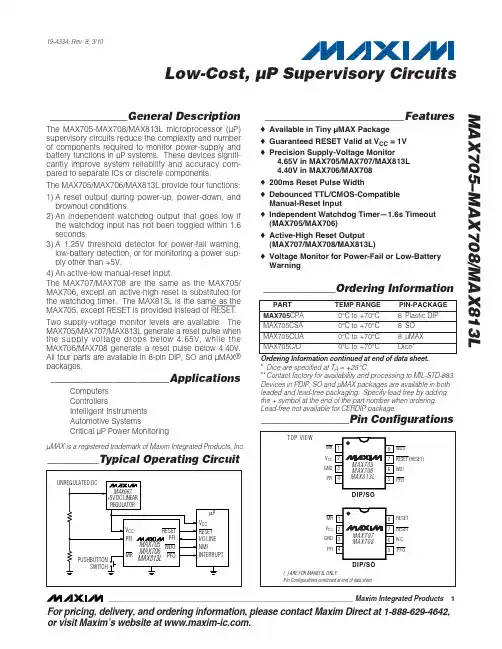
功能监控器MAX705/706/813中文资料。
概述MAX705/706/813L是一组CMOS监控电路,能够监控电源电压、电池故障和微处理器(MPU或mP)或微控制器(MCU或mC)的工作状态。
将常用的多项功能集成到一片8脚封装的小芯片内,与采用分立元件或单一功能芯片组合的电路相比,大大减小了系统电路的复杂性和元器件的数量,显著提高了系统可靠性和精确度。
该系列产品采用3种不同的8脚封装形式:DIP、SO和mMAX。
主要应用于:微处理器和微控制器系统;嵌入式控制器系统;电池供电系统;智能仪器仪表;通信系统;寻呼机;蜂窝移动电话机;手持设备;个人数字助理(PDA);电脑电话机和无绳电话机等等。
功能说明RESET/RESET操作复位信号用于启动或者重新启动MPU/MCU,令其进入或者返回到预知的循环程序并顺序执行。
一旦MPU/MCU处于未知状态,比如程序“跑飞”或进入死循环,就需要将系统复位。
对于MAX705和MAX706而言,在上电期间只要Vcc大于,就能保证输出电压不高于的低电平。
在Vcc上升期间RESET维持低电平直到电源电压升至复位门限或以上。
在超过此门限后,内部定时器大约再维持200ms后释放RESET,使其返回高电平。
无论何时只要电源电压降低到复位门限以下(即电源跌落),RESET引脚就会变低。
如果在已经开始的复位脉冲期间出现电源跌落,复位脉冲至少再维持140ms。
在掉电期间,一旦电源电压Vcc降到复位门限以下,只要Vcc不比还低,就能使RESET维持电压不高于的低电平。
MAX705和MAX706提供的复位信号为低电平RESET,而MAX813L提供的复位信号为高电平RESET,三者其它功能完全相同。
有些单片机,如INTEL的80C51系列,需要高电平有效的复位信号。
看门狗定时器MAX705/706/813L片内看门狗定时器用于监控MPU/MCU的活动。
如果在内WDI端没有收到来自MPU/MCU 的触发信号,并且WDI处于非高阻态,则WDO输出变低。
General DescriptionThe MAX17005A/MAX17006A/MAX17015A are high-fre-quency multichemistry battery chargers. These circuits feature a new high-frequency current-mode architecture that significantly reduces component size and cost*.The charger uses a high-side MOSF ET with n-channel synchronous rectifier. Widely adjustable charge current,charge voltage, and input current limit simplify the con-struction of highly accurate and efficient chargers.The charge voltage and charge current are set with analog control inputs. The charge current setting can also be adjusted with a PWM input. High-accuracy cur-rent-sense amplifiers provide fast cycle-by-cycle cur-rent-mode control to protect against short circuits to the battery and respond quickly to system load transients.In addition, the charger provides a high-accuracy ana-log output that is proportional to the adapter current. In the MAX17015A, this current monitor remains active when the adapter is absent to monitor battery dis-charge current.The MAX17005A charges three or four Li+ series cells,and the MAX17006A charges two or three Li+ series cells. The MAX17015A adjusts the charge voltage set-ting and the number of cells through a feedback resis-tor-divider from the output. All variants of the charger can provide at least 4A of charge current with a 10m Ωsense resistor.The charger utilizes a charge pump to control an n-channel adapter selection switch. The charge pump remains active even when the charger is off. When the adapter is absent, a p-channel MOSFET selects the battery.The MAX17005A/MAX17006A/MAX17015A are avail-able in a small, 4mm x 4mm x 0.8mm 20-pin, lead-free TQFN package. An evaluation kit is available to reduce design time.ApplicationsNotebook Computers Tablet PCsPortable Equipment with Rechargeable BatteriesFeatureso High Switching Frequency (1.2MHz)o Controlled Inductor Current-Ripple ArchitectureReduced BOM CostSmall Inductor and Output Capacitors o ±0.4% Accurate Charge Voltage o ±2.5% Accurate Input-Current Limiting o ±3% Accurate Charge Current o Single-Point Compensationo Monitor Outputs for±2.5% Accurate Input Current Limit ±2.5% Battery Discharge Current (MAX17015A Only)AC Adapter Detectiono Analog/PWM Adjustable Charge-Current Setting o Battery Voltage Adjustable for 3 and 4 Cells(MAX17005A) or 2 and 3 Cells (MAX17006A)o Adjustable Battery Voltage (4.2V to 4.4V/Cell)o Cycle-by-Cycle Current LimitBattery Short-Circuit Protection Fast Response for Pulse ChargingFast System-Load-Transient Response o Programmable Charge Current < 5Ao Automatic System Power Source Selection withn-Channel MOSFET o Internal Boost Diodeo +8V to +26V Input-Voltage RangeMAX17005A/MAX17006A/MAX17015A1.2MHz, Low-Cost,High-Performance Chargers________________________________________________________________Maxim Integrated Products1Ordering Information19-4355; Rev 0; 10/08For pricing, delivery, and ordering information,please contact Maxim Direct at 1-888-629-4642,or visit Maxim’s website at .*Future product—contact factory for availability.**EP = Exposed pad.Pin Configuration and Minimal Operating Circuit appear at end of data sheet.*Patent pending.M A X 17005A /M A X 17006A /M A X 17015A1.2MHz, Low-Cost,High-Performance ChargersABSOLUTE MAXIMUM RATINGSELECTRICAL CHARACTERISTICSStresses beyond those listed under “Absolute Maximum Ratings” may cause permanent damage to the device. These are stress ratings only, and functional operation of the device at these or any other conditions beyond those indicated in the operational sections of the specifications is not implied. Exposure to absolute maximum rating conditions for extended periods may affect device reliability.DCIN, CSSP, CSSN, BATT, CSIN, CSIP, ACOK,LX to AGND.......................................................-0.3V to +30V BST to LDO.............................................................-0.3V to +30V CSIP to CSIN, CSSP to CSSN ..............................-0.3V to +0.3V IINP, FB, ACIN to AGND.............................-0.3V to (V AA + 0.3V)V AA , LDO, ISET, VCTL, CC to AGND.......................-0.3V to +6V DHI to LX....................................................-0.3V to (BST + 0.3V)BST to LX..................................................................-0.3V to +6VDLO to PGND............................................-0.3V to (LDO + 0.3V)PGND to AGND....................................................-0.3V to +0.3V Continuous Power Dissipation (T A = +70°C)16-Pin TQFN (derate 16.9mW/°C above +70°C)....1349.1mW Operating Temperature Range ...........................-40°C to +85°C Junction Temperature......................................................+150°C Storage Temperature Range.............................-60°C to +150°C Lead Temperature (soldering, 10s).................................+300°CIIIELECTRICAL CHARACTERISTICS (continued)MAX17005A/MAX17006A/MAX17015A1.2MHz, Low-Cost,High-Performance Chargers(Circuit of Figure 1, V DCIN= V CSSP= V CSSN= 19V, V BATT= V CSIP= V CSIN= 16.8V, V VCTL= V AA, V ISET= 1V, T A= 0°C to +85°C, Array_______________________________________________________________________________________3M A X 17005A /M A X 17006A /M A X 17015A1.2MHz, Low-Cost,High-Performance Chargers 4_______________________________________________________________________________________ELECTRICAL CHARACTERISTICS (continued)(Circuit of Figure 1, V DCIN = V CSSP = V CSSN = 19V, V BATT = V CSIP = V CSIN = 16.8V, V VCTL = V AA , V ISET = 1V, T A = 0°C to +85°C ,ELECTRICAL CHARACTERISTICS(Circuit of Figure 1, V = V = V = 19V, V = V = V = 16.8V, V = V , V = 1V, T = -40°C to +85°C ,ELECTRICAL CHARACTERISTICS (continued)MAX17005A/MAX17006A/MAX17015A1.2MHz, Low-Cost,High-Performance Chargers(Circuit of Figure 1, V DCIN= V CSSP= V CSSN= 19V, V BATT= V CSIP= V CSIN= 16.8V, V VCTL= V AA, V ISET= 1V, T A= -40°C to +85°C,M A X 17005A /M A X 17006A /M A X 17015A1.2MHz, Low-Cost,High-Performance Chargers 6_______________________________________________________________________________________ELECTRICAL CHARACTERISTICS (continued)(Circuit of Figure 1, V DCIN = V CSSP = V CSSN = 19V, V BATT = V CSIP = V CSIN = 16.8V, V VCTL = V AA , V ISET = 1V, T A = -40°C to +85°C ,DCIN BATT V DCIN = 16V, V BATT = 16.8V.MAX17005A/MAX17006A/MAX17015A1.2MHz, Low-Cost,High-Performance Chargers_______________________________________________________________________________________7Typical Operating Characteristics(Circuit of Figure 1, adapter = 19V, battery = 10V, ISET = 1.05V, V CTL = GND, T A = +25°C, unless otherwise noted.)IINP DC ERROR vs. SYSTEM CURRENTSYSTEM CURRENT (A)I I N P E R R O R (%)4312-8-6-4-20246810-105IINP ERRORvs. SYSTEM CURRENTSYSTEM CURRENT (A)I I N P E R R O R (%)4.03.52.5 3.01.0 1.5 2.00.5-8-6-4-20246810-100 4.5ISET PWM DUTY-CYCLE CHANGEDUTY CYCLEC H A R G E -C U R R E N T E R R O R (%)0.80.90.10.20.30.40.50.60.70.51.01.52.02.53.0001.0ISET PWM DUTY-CYCLE CHANGEDUTY CYCLEC H A R G E C U R R E N T (A )8090102030405060700.51.01.52.02.53.03.500100ISET PWM FREQUENCY SWEEPFREQUENCY (kHz)C H A R G E -C U R R E N T E R R O R (%)6007001002003004005000.51.01.52.02.53.00800BATTERY VOLTAGE-SETTING ERRORVCTL (V)B A T T E R Y V O L T A G E E R R O R (%)3.03.54.00.5 1.0 1.5 2.0 2.5-0.5-0.4-0.3-0.2-0.10-0.60 4.5SYSTEM LOAD TRANSIENTMAX17005A toc07200μs/divSYSTEM CURRENT 5A/divCHARGING CURRENT 5A/div INDUCTOR CURRENT5A/divEFFICIENCYvs. CHARGE CURRENTCHARGE CURRENT (A)E F F I C I E N C Y (%)2.53.0 3.50.5 1.0 1.5 2.070657580859590100600 4.0V AA LOAD REGULATIONLOAD CURRENT (mA)V A A V O L T A G E (V )0.80.20.40.64.1974.1964.1984.2004.1994.2014.2034.2024.2054.2044.1951.0M A X 17005A /M A X 17006A /M A X 17015A1.2MHz, Low-Cost,High-Performance Chargers 8_______________________________________________________________________________________LDO LOAD REGULATIONLDO CURRENT (mA)L D O V O L T A G E (V )35510152025305.355.405.455.505.3040LDO LINE REGULATIONINPUT VOLTAGE (V)L D O V O L T A G E (V )24221012141618205.355.405.455.505.30826V AA vs. TEMPERATURETEMPERATURE (°C)V A A (V )6080-40-2020404.19704.19804.19754.19854.19954.19904.20054.20004.1965-60100HIGH-SIDE MOSFET OFF-TIME ANDSWITCHING FREQUENCY vs. BATTERY VOLTAGEBATTERY VOLTAGE (V)S W I T C H I N G F R E Q U E N C Y (M H z )H I G H -S I D E M O S F T E O F F -T I M E (μs )1614101246820.20.40.60.81.01.21.41.6018ADAPTER REMOVALMAX17005A toc16200ms/div5.00V 5.00V 5.00VADAPTER CURRENT vs. ADAPTER VOLTAGEADAPTER VOLTAGE (V)A D A P T E R C U R R E N T (m A )155100.20.40.60.81.01.21.41.60020BATTERY LEAKAGEBATTERY VOLTAGE (V)B A T T E R Y L E A K A G EC U R R E N T (μA )14161868241012501001502002503003504000020Typical Operating Characteristics (continued)(Circuit of Figure 1, adapter = 19V, battery = 10V, ISET = 1.05V, V CTL = GND, T A = +25°C, unless otherwise noted.)MAX17005A/MAX17006A/MAX17015A1.2MHz, Low-Cost,High-Performance Chargers_______________________________________________________________________________________9M A X 17005A /M A X 17006A /M A X 17015A1.2MHz, Low-Cost,High-Performance Chargers 10______________________________________________________________________________________Figure 1. Typical Operating CircuitDetailed DescriptionThe MAX17005A/MAX17006A/MAX17015A include all the functions necessary to charge Li+, NiMH, and NiCd batteries. An all n-channel synchronous-rectified step-down DC-DC converter is used to implement a preci-sion constant-current, constant-voltage charger. The charge current and input current-limit sense amplifiers have low-input offset errors (250μV typ), allowing the use of small-valued sense resistors.The MAX17005A/MAX17006A/MAX17015A use a new thermally optimized high-frequency architecture. With this new architecture, the switching frequency is adjusted to control the power dissipation in the high-side MOSF ET. Benefits of the new architecture include:reduced output capacitance and inductance, resulting in smaller printed-circuit board (PCB) area and lower cost.Figure 2. Functional DiagramThe MAX17005A/MAX17006A/MAX17015A feature a voltage-regulation loop (CCV) and two current-regula-tion loops (CCI and CCS). The loops operate indepen-dently of each other. The CCV voltage-regulation loop monitors BATT to ensure that its voltage never exceeds the voltage set by VCTL. The CCI battery charge cur-rent-regulation loop monitors current delivered to BATT to ensure that it never exceeds the current limit set by ISET. The charge current-regulation loop is in control as long as the battery voltage is below the set point. When the battery voltage reaches its set point, the voltage-regulation loop takes control and maintains the battery voltage at the set point. A third loop (CCS) takes control and reduces the charge current when the adapter cur-rent exceeds the input current limit.The MAX17005A/MAX17006A/MAX17015A have single-point compensation. The two current loops are internal-ly compensated while the voltage loop is compensated with a series RC network at CC pin. See the CC Loop Compensation section for the resistor and capacitor selection. A functional diagram is shown in Figure 2.MAX17005A/MAX17006A/MAX17015A1.2MHz, Low-Cost,High-Performance ChargersM A X 17005A /M A X 17006A /M A X 17015A1.2MHz, Low-Cost,High-Performance Chargers Setting Charge VoltageThe VCTL input adjusts the battery-output voltage,V BATT , and determines the number of cells. For 3- and 4-cell applications, use the MAX17005A; for 2- and 3-cell applications, use the MAX17006A. Use the MAX17015A to adjust the cell number and set the cell voltage with a resistive voltage-divider from the output.Based on the version of the part, the number of cells and the level of VCTL should be set as in Table 1:The MAX17005A/MAX17006A support from 4.2V/cell to4.4V/cell, whereas the MAX17015A supports minimum 2.1V. The maximum voltage is determined with the dropout performance of IC. When the required voltage falls outside the range available with the MAX17005A or MAX17006A, the MAX17015A should be used.The charge-voltage regulation for the MAX17005A and MAX17006A is calculated with the following equations:for 3-cell selection of MAX17005A and MAX17006A,4.2V > VCTL > 2.4V:for 2- or 4-cell selection of MAX17006A or MAX17005A,respectively, 0 < VCTL < 1.8V. Connect VCTL to GND or to V AA for default 4.2V/cell battery-voltage setting.For the MAX17015A, connect VCTL to GND to set the FB regulation point to 2.1V. The charge-voltage regulation is calculated with the following equation:There are two constraints in choosing R7 and R8. The resistors cannot be too small since they discharge the battery, and they cannot be too large because FB pin consumes less than 1μA of input bias current. Pick R8to be approximately 10k Ωand then calculate R7.FB regulation error (±0.5% max) and the tolerance of R7and R8 both contribute to the error on the battery volt-age. Use 0.1% feedback resistors for best accuracy.Setting Charge CurrentThe voltage at ISET determines the voltage across cur-rent-sense resistor RS2. ISET can accept either analog or digital inputs. The full-scale differential voltage between CSIP and CSIN is 80mV (8A for RS2 = 10m Ω)for the analog input, and 60mV (6A for RS2 = 10m Ω) for the digital PWM input.When the MAX17005A/MAX17006A/MAX17015A power up and the charger is ready, if there is no clock edge within 20ms, the circuit assumes ISET is an analog input, and disables the PWM filter block. To configure the charge current, force the voltage on ISET according to the following equation:The input range for ISET is from 0 to V AA /2. To shut down the charger, pull ISET below 26mV.If there is a clock edge on ISET within 20ms, the PWM filter is enabled and ISET accepts digital PWM input.The PWM filter has a DAC with 8-bit resolution that cor-responds to equivalent V CSIP-CSINsteps.Figure 3. The MAX17015A Charge-Voltage Regulation Feedback NetworkMAX17005A/MAX17006A/MAX17015A1.2MHz, Low-Cost,High-Performance ChargersThe PWM filter accepts the digital signal with a frequency from 128Hz to 500kHz. Zero duty cycle shuts down the MAX17005A/MAX17006A/MAX17015A, and 99.5% duty cycle corresponds to full scale (60mV) across CSIP and CSIN.Choose a current-sense resistor (RS2) to have a suffi-cient power-dissipation rating to handle the full-charge current. The current-sense voltage can be reduced to minimize the power-dissipation period. However, this can degrade accuracy due to the current-sense amplifier’s input offset (0.25mV typ). See Typical Operating Characteristics to estimate the charge-current accuracy at various set points.Setting Input-Current LimitThe total input current, from a wall adapter or other DC source, is the sum of the system supply current and the current required by the charger. When the input current exceeds the set input-current limit, the controller decreases the charge current to provide priority to sys-tem load current. System current normally fluctuates as portions of the system are powered up or down. The input-current-limit circuit reduces the power require-ment of the AC wall adapter, which reduces adapter cost. As the system supply rises, the available charge current drops linearly to zero. Thereafter, the total input current can increase without limit.The total input current is the sum of the device supply cur-rent, the charger input current, and the system load cur-rent. The total input current can be estimated as follows:where ηis the efficiency of the DC-to-DC converter (typically 85% to 95%).In the MAX17005A/MAX17006A/MAX17015A, the volt-age across CSSP and CSSN is constant at 60mV.Choose the current-sense resistor, RS1, to set the input current limit. F or example, for 4A input current limit,choose RS1 = 15m Ω. F or the input current-limit set-tings, which cannot be achievable with standard sense resistor values, use a resistive voltage-divider between CSSP and CSSN to tune the setting (Figure 4).To minimize power dissipation, first choose RS1according to the closest available value. F or conve-nience, choose Ra = 6k Ωand calculate Rb from the above equation.Choose a current-sense resistor (RS1) to have a suffi-cient power rating to handle the full system current. The current-sense resistor can be reduced to improve effi-ciency, but this degrades accuracy due to the current-sense amplifier’s input offset (0.15mV typ). See Typical Operating Characteristics to estimate the input current-limit accuracy at various set points.Automatic Power-Source SelectionThe MAX17005A/MAX17006A/MAX17015A use an external charge pump to drive the gate of an n-channel adapter selection switch (N3 and Q1a). In F igure 1,when the adapter is present, BST is biased 5V above V ADAPTER so that N3 and Q1a are on, and Q1b is off.As long as the adapter is present, even though the charger is off, the power stage forces a refresh pulse to the BST charge pump every 5ms.When the adapter voltage is removed, the charger stops generating BST refresh pulses and N4 forces N2off, Q1b turns on and supplies power to the system from the battery.In Figure 1, D1 must have low forward-voltage drop and low reverse-leakage current to ensure sufficient gate drive at N3 and Q1a. A 100mA, low reverse-leakage Schottky diode is the right choice.Analog Input Current-Monitor OutputUse IINP to monitor the system-input current, which issensed across CSSP and CSSN. The voltage at IINP is proportional to the input current:where I INPUT is the DC current supplied by the AC adapter, G IINP is the transconductance of the sense amplifier (2.8mA/V typ), and R IINP is the resistor con-nected between IINP and ground. Typically, IINP has a 0 to 3.5V output-voltage range. Leave IINP unconnectedwhen not used.Figure 4. Input Current-Limit Fine-TuningM A X 17005A /M A X 17006A /M A X 17015A1.2MHz, Low-Cost,High-Performance Chargers IINP can also be used to monitor battery discharge cur-rent (see Figure 5). In the MAX17015A, when the adapter is absent, drive ISET above 1V to enable IINP during bat-tery discharge. When the adapter is reinserted, ISET must be released to the correct control level within 300ms.AC Adapter DetectionThe MAX17005A/MAX17006A/MAX17015A include a hysteretic comparator that detects the presence of an AC power adapter. When ACIN is lower than 2.1V, the open-drain ACOK output becomes high impedance.Connect a 10k Ωpullup resistance between LDO and ACOK . Use a resistive voltage-divider from the adapter’s output to the ACIN pin to set the appropriate detection threshold. Select the resistive voltage-divider so that the voltage on ACIN does not to exceed its absolute maximum rating (6V).LDO Regulator and V AAAn integrated low-dropout (LDO) linear regulator pro-vides a 5.4V supply derived from DCIN, and delivers over 40mA of load current. Do not use the LDO to external loads greater than 10mA. The LDO powers the gate drivers of the n-channel MOSF ETs. See the MOSFET Drivers section. Bypass LDO to PGND with a 4.7μF ceramic capacitor. V AA is 4.2V reference sup-plied by DCIN. V AA biases most of the control circuitry,and should be bypassed to GND with a 1μF or greater ceramic capacitor.Operating ConditionsThe MAX17005A/MAX17006A/MAX17015A have the fol-lowing operating states:•Adapter Present:When DCIN is greater than 8.7V,the controller detects the adapter. In this condition,both the LDO and V AA turn on and battery charging is allowed:a) Charging:The total MAX17005A/MAX17006A/MAX17015A quiescent current when charging is 3mA (max) plus the current required to drive the MOSFETs.b) Not Charging:To disable charging drive ISET below 26mV. When the adapter is present and charging is disabled, the total adapter quiescent current is less than 1.5mA and the total battery quiescent current is less than 60μA. The charge pump still operates.•Adapter Absent (Power Fail):When V DCIN is less than V CSIN + 120mV, the DC-DC converter is in dropout. The charger detects the dropout condition and shuts down.The MAX17005A/MAX17006A/MAX17015A allow charging under the following conditions:•DCIN > 7.5V, LDO > 4V, V AA > 3.1V •V DCIN > V CSIN + 420mV (300mV falling hysteresis)•V ISET > 45mV or PWM detected____________________DC-DC ConverterThe MAX17005A/MAX17006A/MAX17015A employ a synchronous step-down DC-DC converter with an n-channel high-side MOSF ET switch and an n-channel low-side synchronous rectifier. The charger features a controlled inductor current-ripple architecture, current-mode control scheme with cycle-by-cycle current limit.The controller’s off-time (t OFF ) is adjusted to keep the high-side MOSF ET junction temperature constant. In this way, the controller switches faster when the high-side MOSF ET has available thermal capacity. This allows the inductor current ripple and the output-volt-age ripple to decrease so that smaller and cheaper components can be used. The controller can also oper-ate in discontinuous conduction mode for improved light-load efficiency.Figure 5. Current-Monitoring Design Battery DischargeThe operation of the DC-to-DC controller is determined by the following five comparators as shown in the func-tional diagram in Figures 2 and 6:•The IMIN comparator triggers a pulse in discontinu-ous mode when the accumulated error is too high.IMIN compares the control signal (LVC) against 10mV (referred at V CSIP - V CSIN). When LVC is less than this threshold, DHI and DLO are both forced low. Indirectly, IMIN sets the peak inductor current in discontinuous mode.•The CCMP comparator is used for current-mode regulation in continuous-conduction mode. CCMP compares LVC against the inductor current. The high-side MOSF ET on-time is terminated when the CSI voltage is higher than LVC.•The IMAX comparator provides a secondary cycle-by-cycle current limit. IMAX compares CSI to 110mV (corresponding to 11A when RS2 = 10mΩ).The high-side MOSFET on-time is terminated when the current-sense signal exceeds 11A. A new cycle cannot start until the IMAX comparator’s output goes low.•The ZCMP comparator provides zero-crossing detec-tion during discontinuous conduction. ZCMP com-pares the current-sense feedback signal to 1A (RS2 = 10mΩ). When the inductor current is lower than the 1A threshold, the comparator output is high, and DLO is turned off.•The OVP comparator is used to prevent overvoltage at the output due to battery removal. OVP com-pares BATT against the VCTL. When BATT is 100mV/cell above the set value, the OVP compara-tor output goes high, and the high-side MOSF ET on-time is terminated. DHI and DLO remain off until the OVP condition is removed.Figure 6. DC-DC Converter Functional DiagramMAX17005A/MAX17006A/MAX17015A1.2MHz, Low-Cost,High-Performance ChargersM A X 17005A /M A X 17006A /M A X 17015A1.2MHz, Low-Cost,High-Performance Chargers CC, CCI, CCS, and LVC Control BlocksThe MAX17005A/MAX17006A/MAX17015A control input current (CCS control loop), charge current (CCI control loop), or charge voltage (CC control loop),depending on the operating condition. The three con-trol loops, CC, CCI, and CCS are brought together internally at the lowest voltage clamp (LVC) amplifier.The output of the LVC amplifier is the feedback control signal for the DC-DC controller. The minimum voltage at the CC, CCI, or CCS appears at the output of the LVC amplifier and clamps the other control loops to within 0.3V above the control point. Clamping the other two control loops close to the lowest control loop ensures fast transition with minimal overshoot when switching between different control loops (see the Compensation section). The CCS and CCI loops are compensated internally, and the CC loop is compen-sated externally.Continuous-Conduction ModeWith sufficiently large charge current, the MAX17005A/MAX17006A/MAX17015s’ inductor current never cross-es zero, which is defined as continuous-conduction mode. The controller starts a new cycle by turning on the high-side MOSF ET and turning off the low-side MOSF ET. When the charge-current feedback signal (CSI) is greater than the control point (LVC), the CCMP comparator output goes high and the controller initiates the off-time by turning off the high-side MOSF ET and turning on the low-side MOSF ET. The operating fre-quency is governed by the off-time and is dependent upon V CSIN and V DCIN .The on-time can be determined using the following equation:where:The switching frequency can then be calculated:At the end of the computed off-time, the controller initi-ates a new cycle if the control point (LVC) is greater than 10mV (V CSIP - V CSIN referred), and the charge current is less than the cycle-by-cycle current limit.Restated another way, IMIN must be high, IMAX must be low, and OVP must be low for the controller to initi-ate a new cycle. If the peak inductor current exceeds IMAX comparator threshold or the output voltage exceeds the OVP threshold, then the on-time is termi-nated. The cycle-by-cycle current limit effectively pro-tects against overcurrent and short-circuit faults.If during the off-time the inductor current goes to zero,the ZCMP comparator output pulls high, turning off the low-side MOSF ET. Both the high- and low-side MOSFETs are turned off until another cycle is ready to begin. ZCOMP causes the MAX17005A/MAX17006A/MAX17015A to enter into the discontinuous conduction mode (see the Discontinuous Conduction section).Discontinuous ConductionThe MAX17005A/MAX17006A/MAX17015A can also operate in discontinuous conduction mode to ensure that the inductor current is always positive. The MAX17005A/MAX17006A/MAX17015A enter discontinuous conduction mode when the output of the LVC control point falls below 10mV (referred at V CSIP - V CSIN ). For RS2 = 10m Ω, this corresponds to a peak inductor current of 1A.In discontinuous mode, a new cycle is not started until the LVC voltage rises above IMIN. Discontinuous mode operation can occur during conditioning charge of overdischarged battery packs, when the charge cur-rent has been reduced sufficiently by the CCS control loop, or when the charger is in constant-voltage mode with a nearly full battery pack.CompensationThe charge voltage, charge current, and input current-limit regulation loops are compensated separately. The charge current and input current-limit loops, CCI and CCS, are compensated internally, whereas the chargevoltage loop is compensated externally at CC.MAX17005A/MAX17006A/MAX17015A1.2MHz, Low-Cost,High-Performance ChargersCC Loop CompensationThe simplified schematic in F igure 7 is sufficient to describe the operation of the controller’s voltage loop,CC. The required compensation network is a pole-zero pair formed with C CC and R CC . The zero is necessary to compensate the pole formed by the output capacitor and the load. R ESR is the equivalent series resistance (ESR) of the charger output capacitor (C OUT ). R L is the equivalent charger output load, where R L = ΔV BATT /ΔI CHG . The equivalent output impedance of the GMV amplifier, R OGMV , is greater than 10M Ω. The voltage-amplifier transconductance, GMV = 0.125μA/mV. The DC-DC converter transconductance is dependent upon charge current-sense resistor RS2:where A CSI = 20, and RS2 = 10m Ωin the typical appli-cation circuits, so GM OUT = 5A/V.The loop transfer function is given by:The poles and zeros of the voltage-loop transfer function are listed from lowest frequency to highest frequency in Table 2.Near crossover, C CC is much lower impedance than R OGMV . Since C CC is in parallel with R OGMV, C CC domi-nates the parallel impedance near crossover. Additionally,R CC is much higher impedance than C CC and dominates the series combination of R CC and C CC , so:C OUT is also much lower impedance than R L near crossover so the parallel impedance is mostly capaci-tive and:Figure 7. CC Loop Diagram。