The infrared conductivity of Na$_x$CoO$_2$ evidence of gapped states
- 格式:pdf
- 大小:523.37 KB
- 文档页数:11
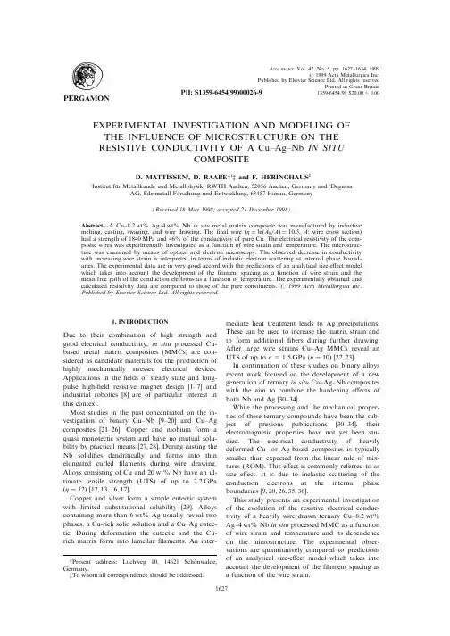
EXPERIMENTAL INVESTIGATION AND MODELING OFTHE INFLUENCE OF MICROSTRUCTURE ON THERESISTIVE CONDUCTIVITY OF A Cu±Ag±Nb IN SITUCOMPOSITED.MATTISSEN1,D.RAABE{1{and F.HERINGHAUS21Institut fu r Metallkunde und Metallphysik,RWTH Aachen,52056Aachen,Germany and2Degussa AG,Edelmetall Forschung und Entwicklung,63457Hanau,Germany(Received18May1998;accepted21December1998)AbstractÐA Cu±8.2wt%Ag±4wt%Nb in situ metal matrix composite was manufactured by inductive melting,casting,swaging,and wire drawing.The®nal wire( ln A0a A 10X5,A:wire cross section) had a strength of1840MPa and46%of the conductivity of pure Cu.The electrical resistivity of the com-posite wires was experimentally investigated as a function of wire strain and temperature.The microstruc-ture was examined by means of optical and electron microscopy.The observed decrease in conductivity with increasing wire strain is interpreted in terms of inelastic electron scattering at internal phase bound-aries.The experimental data are in very good accord with the predictions of an analytical size-e ect model which takes into account the development of the®lament spacing as a function of wire strain and the mean free path of the conduction electrons as a function of temperature.The experimentally obtained and calculated resistivity data are compared to those of the pure constituents.#1999Acta Metallurgica Inc. Published by Elsevier Science Ltd.All rights reserved.1.INTRODUCTIONDue to their combination of high strength and good electrical conductivity,in situ processed Cu-based metal matrix composites(MMCs)are con-sidered as candidate materials for the production of highly mechanically stressed electrical devices. Applications in the®elds of steady state and long-pulse high-®eld resistive magnet design[1±7]and industrial robotics[8]are of particular interest in this context.Most studies in the past concentrated on the in-vestigation of binary Cu±Nb[9±20]and Cu±Ag composites[21±26].Copper and niobium form a quasi monotectic system and have no mutual solu-bility by practical means[27,28].During casting the Nb solidi®es dendritically and forms into thin elongated curled®laments during wire drawing. Alloys consisting of Cu and20wt%Nb have an ul-timate tensile strength(UTS)of up to 2.2GPa (Z 12)[12,13,16,17].Copper and silver form a simple eutectic system with limited substitutional solubility[29].Alloys containing more than6wt%Ag usually reveal two phases,a Cu-rich solid solution and a Cu±Ag eutec-tic.During deformation the eutectic and the Cu-rich matrix form into lamellar®laments.An inter-mediate heat treatment leads to Ag precipitations. These can be used to increase the matrix strain and to form additional®bers during further drawing. After large wire strains Cu±Ag MMCs reveal an UTS of up to s=1.5GPa(Z 10)[22,23].In continuation of these studies on binary alloys recent work focused on the development of a new generation of ternary in situ Cu±Ag±Nb composites with the aim to combine the hardening e ects of both Nb and Ag[30±34].While the processing and the mechanical proper-ties of these ternary compounds have been the sub-ject of previous publications[30±34],their electromagnetic properties have not yet been stu-died.The electrical conductivity of heavily deformed Cu-or Ag-based composites is typically smaller than expected from the linear rule of mix-tures(ROM).This e ect is commonly referred to as size e ect.It is due to inelastic scattering of the conduction electrons at the internal phase boundaries[9,20,26,35,36].This study presents an experimental investigation of the evolution of the resistive electrical conduc-tivity of a heavily wire drawn ternary Cu±8.2wt% Ag±4wt%Nb in situ processed MMC as a function of wire strain and temperature and its dependence on the microstructure.The experimental obser-vations are quantitatively compared to predictions of an analytical size-e ect model which takes into account the development of the®lament spacing as a function of the wire strain.Acta mater.Vol.47,No.5,pp.1627±1634,1999#1999Acta Metallurgica Inc.Published by Elsevier Science Ltd.All rights reservedPrinted in Great Britain1359-6454/99$20.00+0.00PII:S1359-6454(99)00026-9{Present address:Luchweg10,14621Scho nwalde,Germany.{To whom all correspondence should be addressed.16272.SAMPLE PREPARATIONA Cu±8.2wt%Ag±4wt%Nb alloy was prepared by inductive melting using a frequency of 10kHz and a power of 50kW [33].All constituents had an initial purity of at least 99.995%.Ingots of 18mm diameter were cast under an argon atmosphere at a pressure of 0.6Â105Pa.A crucible and a mould of high purity graphite were used.The mould was pre-heated to about 6008C to ensure good ¯uidity and ®lling.From the cast cylindrical ingots wires were produced by rotary swaging and drawing through hard metal drawing bench dies.A maximum true wire strain above Z 10(Z ln A 0a A ,A :wire cross section)was attained without intermediate annealing.Further processing details are reported elsewhere [33,37].3.EXPERIMENTAL PROCEDURE3.1.Experimental investigation of the microstructure Optical and scanning electron microscopy (SEM)were used to determine the morphology and top-ology both of the Cu matrix and of the Ag and Nb ®laments.Due to insu cient contrast,an unam-biguous optical identi®cation of the various phases was sometimes not possible.The samples were thus additionally analyzed using energy-disperse X-rayspectrometry (EDX).The morphology of the iso-lated Nb ®bers was also investigated by use of a selective etching technique,where the Cu and Ag were dissolved by dilute nitric acid.Details about the experimental procedure were reported previously [32].3.2.Experimental investigation of the resistive elec-trical conductivitySystematic measurements of the resistive conduc-tivity at 298and 77K as a function of the wire strain were carried out for Cu±8.2wt%Ag±4wt%Nb by means of the direct current (d.c.)four-probe technique using a sample current of 100mA.For a number of Cu±8.2wt%Ag±4wt%Nb,pure Cu,pure Ag,and pure Nb wires of identical total wire strain;the in¯uence of the temperature on the resis-tive conductivity was studied within the temperature range 3±350K.4.EXPERIMENTAL RESULTS4.1.Microstructure evolution as a function of wire strainFigure 1shows the development of the diameters of the Cu matrix phase (d Cu ),the Nb ®laments (d Nb ),and the Ag ®laments (d Ag )in thecompositeFig.1.Development of the diameters of the Nb ®laments,the Ag ®laments,and the Cu matrix phasein the Cu±8.2wt%Ag±4wt%Nb composite as investigated by quantitative SEM.MATTISSEN et al.:Cu±Ag±Nb IN SITU COMPOSITE1628as a function of the true wire strain Z .At low strains the Ag ®laments were thicker and shorter than the Nb ®laments.With increasing strain their average thickness became more similar to that of the Nb ®laments.At a wire strain of Z 3X 6the average Ag ®lament diameter amounted to d Ag I 676nm and at Z 6to d Ag I 260nm.At a wire strain of Z 2X 6the average Nb ®lament diameter amounted to d Nb I 529nm and at Z 9X 5to d Nb I 66nm.For including the evolution of the ®lament morphology in an analytical size-e ect model the average phase diameters were exponentially ®tted from the metallographic data according to d Cu =31767nm Âexp(À0.6415Z ),d Ag =2630nm Âexp(À0.3861Z ),and d Nb =1386.6nm Âexp(À0.413Z ).4.2.Resistive conductivity as a function of wire strain and temperatureFigure 2shows the dependence of the electrical resistivity of Cu±8.2wt%Ag±4wt%Nb on the strain at 298and 77K.At true wire strains above Z 8X 5the conductivity decreases drastically.The increase in the resistivity with increasing strain is more pronounced at 77K (from H 10n O m at Z 3X 5to H 20n O m at Z I 10)than at 298K (from H 27n O m at Z 3X 5to H 38n O m at Z I 10).Consequently,the resistivity ratio of Cu±8.2wt%Ag±4wt%Nb,r 298K a r 77K ,drops as a func-tion of the true wire strain (Fig.3).At temperatures below the transition temperature of pure Nb the wire drawn Cu±8.2wt%Ag±4wt%Fig.2.Electrical resistivity of the ternary Cu±8.2wt%Ag±4wt%Nb composite as a function of thetrue (logarithmic)wire strain Z (Z ln A 0a A ,A :wire cross section)at T 298and 77K.Fig.3.Electrical resistivity ratio r 298K a r 77K of the ternary Cu±8.2wt%Ag±4wt%Nb compositeas a function of the true (logarithmic)wire strain Z (Z ln A 0a A ,A :wire cross section).MATTISSEN et al.:Cu±Ag±Nb IN SITU COMPOSITE 1629Nb reveals superconducting properties.Figure 4shows for the composite the transition to the super-conducting state as a function of strain.The data reveal that an increasing wire strain leads to a shift of the transition temperature to lower values.A detailed analysis of the superconducting properties of the ternary composite is given in Ref.[38]based on Ginzburg±Landau theory.The electrical resistivity of pure Cu wires and pure Ag wires was practically independent of the degree of deformation and was always lower than for the composite (Fig.5).The e ect of defor-mation on the resistivity temperature coe cient of pure Cu,pure Ag,pure Nb,and Cu±8.2wt%Ag±4wt%Nb is given in Fig.6.While the temperature coe cient of the pure wires is practically indepen-dent on wire strain,that of the composite drops with increasing wire strain.5.MODELING OF THE ELECTRICAL RESISTIVITYOF THE Cu±Ag±Nb COMPOSITE5.1.Fundamentals of the modelAny analytical calculation of absolute values ofthe electrical resistivity of MMCs requires very detailed data both on the impurity content and dis-tribution and on the density and distribution of the lattice defects (e.g.dislocation density,grain size,etc.).Since these data are usually not known with su cient reliablility,analytical models of the resis-tivity of composites are commonly exclusively based on the size e ect,which typically provides by far the most dominant contribution to inelastic internalscattering of the conduction electrons in such materials [9,20,26,35,36].The predictions of such models can then be compared to the relative changes observed experimentally.Analytical predictions of the electrical resistivity of composites on the basis of the size e ect require the volume fractions and the topologies of each phase in the composite and some intrinsic con-stants.The model starts with the calculation of the elec-trical resistivity of each phase according to the phe-nomenological expression for surface and phase boundary scattering given by Sondheimer [39]r d r 0 1 34 1Àpl 0 Td1 where r (d )is the resistivity as a function of the ®la-ment thickness,r 0the resistivity for a sample with-out scattering at phase boundaries (in®nite sampleor phase size),p the scattering factor,l 0the mean free path of the conduction electrons in that par-ticular phase and d the thickness of the ®lament.According to Dingle [35]the scattering factor p rep-resents the probability of elastic scattering and (1Àp )that of inelastic scattering at the phase boundary.The mean free paths of the conduction electrons in the various phases (as a function of temperature)were determined from the temperature dependent resistivities of the bulk phases usings T l 0 T e 2N el "h V 3p 2N elVÀ1a 32Fig.4.Transition of the electrical resistivity of the ternary Cu±8.2wt%Ag±4wt%Nb composite from the normal resistive state to the superconducting state as a function of temperature for two di erent degrees of the true (logarithmic)wire strain (Z 8,Z 5X 96)(Z ln A 0a A ,A :wire cross section).MATTISSEN et al.:Cu±Ag±Nb IN SITU COMPOSITE1630where s (T )is the conductivity and N el /V the elec-tron density.The right-hand side of equation (2)was calculated using a value of N el a V 5X 57Â1029a m 3under the assumption of mono-valence for Ag and Cu and a value of N el a V 5X 325Â1029a m 3for Nb.Finally,the individual resistivities r i of the phases were topologically combined to give the overall res-istivity of the composite r MMC .The model treats all phases as resistors that are arranged parallelr MMCni 1f i r iÀ13where the f i are the volume fractions of the phases i 1,F F F ,n ,and r i the electrical resistivities of the phases i 1,F F F ,n .5.2.Application of the modelThe prediction of the electrical resistivity of the Cu±8.2wt%Ag±4wt%Nb composite on the basis of equations (1)±(3)requires some topologicalcon-Fig.5.Electrical resistivity of pure Cu and pure Ag as a function oftemperature.Fig.6.Temperature coe cient of the electrical resistivity of Cu,Ag,Nb,and the ternary Cu±8.2wt%Ag±4wt%Nb composite between 273and 373K as a function of the true (logarithmic)wire strain Z(Z ln A 0a A ,A :wire cross section).MATTISSEN et al.:Cu±Ag±Nb IN SITU COMPOSITE 1631siderations about the incorporation of the topology of the Ag®laments.In the as-cast sample the Ag had a lamellar shape and formed a Ag±Cu eutectic whilst the Nb was precipitated in the form of iso-lated Wul polyhedra and dendrites[32,33]. Therefore,the composite was treated as a material consisting of two primary phases,namely, 95.82vol.%Cu±Ag and4.18vol.%Nb,in which the former consists of two sub-phases,namely, 91.92vol.%Cu and8.08vol.%Ag.The weight fractions of the primary phases and of the sub-phases were calculated from the weight composition of Cu±8.2wt%Ag±4wt%Nb as(90.66wt%Cu±9.34wt%Ag)±4wt%Nb and the volume fractions correspondingly as(91.92vol.%Cu±8.08vol.% Ag)±4.18vol.%Nb.Equation(3)was®rst applied to the two sub-phases Cu and Ag which then in turn were combined parallel with Nb to form the overall composite.Values for the interface scattering factors p as-sociated with the Cu±Ag interfaces were taken from previous investigations and simulations on this binary system[27].These were for Cu±Ag:p 0X81 at T 298K and p 0X84at T 77K.The size-e ect approach as outlined in equation(1)can be derived from the Boltzmann transport equation for cases where d b l0.This condition holds for the Cu (d Cu a l0Cu I3),the Ag(d Ag a l0Ag I3),and the Nb phase(d Nb a l0Nb I20)corresponding to the current data for Z 10and T 293K.5.3.Predictions of the modelThe predictions of the size-e ect model for the composite,Cu±8.2wt%Ag±4wt%Nb,and for the various phases,Cu,Ag,Cu±Ag,and Nb,are given in Fig.7as a function of the wire strain at T 77K[Fig.7(a)and(b)]and at T 298K[Fig.7(c) and(d)].A strong e ect can be found in the Cu and Ag phases and thus also in Cu±Ag,whereas Nb reveals only weak changes with deformation. Figure7(b)(T 77K)and(d)(T 298K)show that a very good agreement between the model and the experimental data is found at low and elevated strains,particularly for T 298K,while the model slightly underpredicts the resistivity at intermediate strains between Z 6and8.6.DISCUSSIONThe resistivity of Cu±8.2wt%Ag±4wt%Nb increases considerably with the degree of defor-mation.The strong dependence may be chie¯y attributed to the scattering of conduction electrons at the various internal phase boundaries.This e ect becomes particularly pronounced when the average ®lament spacing is,after heavy deformation,of the same order of magnitude as the mean free path of the conduction electrons in the Cu and the Ag phase(Figs2and7)[9,36].Since the mean free electron path linearly decreases as a function of temperature in the regime above the Debye tem-perature,due to the increase of phonon scattering, the contribution of interface scattering to the over-all resistivity is more pronounced at low tempera-tures[Fig.7(b),increase by H100%]than at elevated temperatures[Fig.7(d),increase by H40%].Since the Cu±Ag interfaces have a low,and the Cu±Nb and Ag±Nb interfaces a very high e ect on inelastic scattering,the latter are assumed to be primarily responsible for the observed increase in resistivity.The density of deformation induced lattice dislo-cations is of minor importance for the dependence of the resistivity on wire strain since only their cores add to the electrical resistivity,but contribute only a very small resistivity change per unit length of a dislocation[36,40,41].Here the applied d.c. four-probe technique is not accurate enough to exactly account for such a change.The composite(Cu±8.08vol.%Ag)±4.18vol.% Nb can be described as consisting of two®rst-order phases,95.82vol.%Cu±Ag and4.18vol.%Nb,the former of which consists of two second-order phases,91.8vol.%Cu and8.08vol.%Ag(see Fig.7).Using this approach enables one to make an analytical topological prediction of the size e ect due to interface scattering.A determination of the absolute values of the electrical resistivity is not feasible due to the e ects of impurities and mutual solution.The latter,although of particular import-ance in the Cu±Ag phase,cannot be incorporated owing to the unavailability of appropriate exper-imental data.In this context the slight discrepancy found at in-termediate degrees of deformation between model and experiment[see Fig.7(b)and(d)]may be quali-tatively attributed to deformation-induced changes in the solubility or in the state of precipitation. While changes in the solubility can be explained in terms of the Gibbs±Thomson equation,which relates solubility to interface curvature,changes in the precipitation state can only be attributed to fric-tional heating of the sample during wire drawing. However,both e ects may either not be as domi-nant anymore at high degrees of deformation[i.e. at strain above Z 8,see Fig.7(b)and(d)]due to the dominance of strong interface scattering,or be reverted owing to the presence of a high density of internal interfaces.The latter argument,however,is not covered by experimental evidence and thus is of speculative character.Regarding the e ect of the microstructure of the individual phases on inelastic scattering[Fig.7(a) and(c)],it may be concluded that the size e ects in the Cu phase and in the Ag phase are chie¯y re-sponsible for the observed increase in the electrical resistivity of the Cu±Ag phase and thus ultimately of the ternary composite.In comparison to the Cu phase and the Cu±Ag phase,the size e ect in Ag, particularly at large strains,is much stronger atMATTISSEN et al.:Cu±Ag±Nb IN SITU COMPOSITE 1632F i g .7.M o d e l e d a n d e x p e r i m e n t a l l y o b s e r v e d r e l a t i v e c h a n g e s o f t h e e l e c t r i c a l r e s i s t i v i t y o f C u ,N b ,A g ,a n d t h e t e r n a r y C u ±8.2w t %A g ±4w t %N b c o m p o s i t e a t T 298a n d 77K a s a f u n c t i o n o f t h e t r u e (l o g a r i t h m i c )w i r e s t r a i n Z (Z l n A 0a A ,A :w i r e c r o s s s e c t i o n ).(a )T 77K ,s i z e e e c t m o d e l f o r t h e v a r i o u s p h a s e s a n d f o r t h e c o m p o -s i t e .(b )T 77K ,c o m p a r i s o n b e t w e e n s i z e -e e c t m o d e l a n d e x p e r i m e n t a l d a t a .(c )T 298K ,s i z e -e e c t m o d e l f o r t h e v a r i o u s p h a s e s a n d f o r t h e c o m p o s i t e .(d )T 298K ,c o m p a r i s o n b e t w e e n s i z e -e e c t m o d e l a n d e x p e r i m e n t a l d a t a .MATTISSEN et al.:Cu±Ag±Nb IN SITU COMPOSITE1633T 298K[Fig.7(a)]than at T 77K[Fig.7(c)]. This e ect is due to the stronger temperature-dependence of the mean free electron path in Cu as compared to Ag.7.CONCLUSIONSA ternary in situ Cu±8.2wt%Ag±4wt%Nb MMC was manufactured by melting,casting,swa-ging,and wire drawing.The microstructure was investigated using electron microscopy and EDX. The resistive conductiving properties were examined using four-probe d.c.tests at various temperatures. The main results are:.The ternary MMC was very ductile.A maximum wire strain of Z 10X5was reached without inter-mediate annealing..Wires of the ternary MMC of maximum strain (Z max 10X5)had an UTS of1840MPa and46% of the conductivity of pure Cu(IACS)..The electrical resistivity of the ternary MMC at large strains drastically increased with increasing strain.This was attributed to the size e ect,i.e. to the inelastic scattering of the conduction elec-trons at the internal interfaces..The in¯uence of the size e ect on the course of the electrical resistivity of the ternary MMC was modeled using an analytical solution of the Boltzmann transport equation.At low and very large strains the model was in very good accord with the experimental data.At intermediate strains between Z 6and8the model underpre-dicted the resistivity.This deviation was inter-preted in terms of changes in the solubility and probably in the precipitation state.AcknowledgementsÐThe authors are indebted to G. Gottstein,H.-J.Scheider-Muntau,and J.D.Embury for helpful discussions.One of the authors(D.R.)gratefully acknowledges the®nancial support by the Deutsche Forschungsgemeinschaft through the Heisenberg program and by the National High Magnetic Field Laboratory in Tallahassee,Florida.REFERENCES1.Foner,S.and Bobrov,E.,I.E.E.E.Magn.,1987,24,1059.2.Asano,T.,Sakai,Y.,Inoue,K.,Oshikiri,M.andMaeda,H.,I.E.E.E.Magn.,1992,28,888.3.Heringhaus,F.,Eyssa,Y.M.,Pernambuco-Wise,P.,Bird,M.D.,Gottstein,G.and Schneider-Muntau,H.-J.,Metall.,1996,50,272.4.Embury,J.D.,Hill,M.A.,Spitzig,W.A.and Sakai,Y.,MRS Bull.,1993,8,57.5.Heringhaus, F.,Le ers,R.,Gottstein,G.andSchneider-Muntau,H.-J.,Processing,Properties,and Application of Cast Metal Matrix Composites,TMS Fall Meeting,Vol.1,1996,p.127.6.Schneider-Muntau,H.-J.,I.E.E.E.Trans.Magn.,1982,18,32.7.Wood,J.T.,Embury,J.D.and Ashby,M.F.,Actamater.,1997,45,1099.8.Raabe,D.,Matissen,K.,Miyake,K.,Takahara,H.and Heringhans,F.,in Proc.Int.Conf.``Dialogues at Lake Louise''1997,CompositesÐDesign for Performance,ed.P.S.Nicholson.Eagle Press, Burington,Ontario,Canada,pp.146±154.9.Bevk,J.,Harbison,J.P.and Bell,J.L.,J.appl.Phys.,1978,49,6031.10.Karasek,K.R.and Bevk,J.,J.appl.Phys.,1981,52,1370.11.Funkenbusch,P. D.and Courtney,T.H.,Actametall.,1985,33,913.12.Spitzig,W.A.,Pelton,A.R.and Laabs,F.C.,Actametall.,1987,35,2427.13.Funkenbusch,P.D.,Lee,J.K.and Courtney,T.H.,Metall.Trans.A,1987,18,1249.14.Chumbley,L.S.,Downing,H.L.,Spitzig,W.A.andVerhoeven,J.D.,Mater.Sci.Engng,1989,A117,59.15.Hong,S.I.,Hill,M.A.and Embury,J.D.,Actametall.,1995,43,3313.16.Spitzig,W.A.,Acta metall.,1991,39,1085.17.Spitzig,W.A.,Downing,H.L.,Laabs,F.C.,Gibson,E.D.and Verhoeven,J.D.,Metall.Trans.A,1993,24,7.18.Hangen,U.and Raabe,D.,Acta metall.,1995,43,4075.19.Heringhaus,F.,Raabe,D.and Gottstein,G.,Actametall.,1995,43,1467.20.Raabe,D.,Heringhaus,F.,Hangen,U.and Gottstein,G.,Z.Metallk.,1995,86,405.21.Cline,H.E.and Lee,D.,Acta metall.,1970,18,315.22.Frommeyer,G.and Wassermann,G.,Physica statussolidi(a),1975,27,99.23.Frommeyer,G.and Wassermann,G.,Acta metall.,1975,23,1353.24.Sakai,Y.,Inoue,K.and Maeda,H.,Acta metall.,1995,43,1517.25.Sakai,Y.and Schneider-Muntau,H.-J.,Acta mater.,1997,45,1017.26.Heringhaus,F.,Ph.D.thesis,Institut fu r Metallkundeund Metallphysik,RWTH Aachen,Germany and National High Magnetic Field Laboratory, Tallahassee,U.S.A.,1998.27.Sohn,K.Y.,Ph.D.thesis,Department for MaterialsScience and Engineering,University of Florida, Gainesville,U.S.A.,1997.28.Chakrabati,D.J.and Laughlin,D.E.,Bull.AlloyPhase Diagrams,1982,2,936.29.Terekhov,G.I.and Aleksandrova,L.N.,Izv.Akad.Nauk SSR.Metally,1984,4,210.30.Murray,J.L.,Metall.Trans.A,1984,15,261.31.Spitzig,W.A.,Unpublished data.32.Raabe,D.and Mattissen,D.,Acta mater.,1998,46,5973.33.Raabe,D.and Mattissen,D.,Metall.,1997,51,464.34.Raabe,D.,Mattissen,D.,Miyake,K.,Takahara,H.and Heringhaus,F.,in:Proceedings of an International Conference``Dialogues at Lake Louise,CompositesÐDesign for Performance'',ed.P.S.Nicholson.Eagle Press,Burlington,Ontario,Canada,1997,p.146.35.Dingle,R.B.,Proc.Soc.Lond.Ser.,1950,201,545.36.Raabe,D.,Comput.Mater.Sci.,1995,3,402.37.Mattissen,D.,Diplomarbeit,Institut fu r Metallkundeund Metallphysik,RWTH Aachen,Germany,1997.38.Raabe,D.and Mattissen,D.,Acta mater.,1999,47,769.39.Sondheimer,E.H.,Adv.Phys.,1952,1,1.40.Blewit,T.H.,Coltmann,R.R.and Rebstock,J.K.,Phil.Mag.,1957,2,323.41.Buck,O.,Physica status solidi,1962,2,535.MATTISSEN et al.:Cu±Ag±Nb IN SITU COMPOSITE 1634。
Material Sciences 材料科学, 2021, 11(4), 453-461Published Online April 2021 in Hans. /journal/mshttps:///10.12677/ms.2021.114053二元层状钴掺杂锰氧化物的制备及电催化性能研究龙霞中南大学材料科学与工程学院,湖南长沙收稿日期:2021年3月26日;录用日期:2021年4月21日;发布日期:2021年4月28日摘要锰在地球上的储量丰富、毒性低,且其层状结构具有强可调性,具备巨大的应用潜力。
然而不恰当的电子结构和较低的导带水平阻碍了其在电催化水裂解中的应用,缺陷工程是提高MnO2电子电导率和电化学性能的重要策略。
本文以层状二氧化锰为基体,通过固相烧结掺杂不同比例钴元素制备了一系列二元锰钴氧化物,作为非贵金属OER催化剂。
其中Na-Mn0.5Co0.5O2二元层状锰钴氧化物材料在10 mA∙cm−2处表现出最佳性能,过电势降低至380 mV,Tafel斜率低至55 mV∙dec−1,优于锰钴单金属氧化物催化剂以及其他二元层状锰钴氧化物。
外源元素掺杂提高了本征电子电导率,增加氧化还原活性中心浓度,加速离子扩散和电荷存储转移,从而达到降低过电位的目的。
关键词二元锰钴氧化物层状材料,纳米片,电催化,OERPreparation and ElectrocatalyticPerformance of Binary LayeredCobalt-Doped ManganeseOxideXia LongSchool of Materials Science and Engineering, Central South University, Changsha HunanReceived: Mar. 26th, 2021; accepted: Apr. 21st, 2021; published: Apr. 28th, 2021龙霞Abstract Manganese is abundant on the earth, because of its low toxicity and strong adjustable layer struc-ture; it has huge application potential. However, improper electronic structure and low conduc-tion band level hinder its application in electrocatalytic water splitting. Defect engineering is an important strategy to improve the electronic conductivity and electrochemical performance of MnO 2. In this paper, a series of binary manganese cobalt oxides were prepared by solid-phase sin-tering doped with different proportion of cobalt on layered manganese dioxide as non-noble metal OER catalyst. The Na-Mn 0.5Co 0.5O 2 binary layered manganese cobalt oxide material shows the best performance at 10 mA ∙cm −2, with overpotential reduced to 380 mV and Tafel slope as low as 55 mV ∙dec −1, which is better than the single metal oxide catalyst and other binary layered oxides. Ex-ogenous element doping improves the intrinsic electronic conductivity, increases the concentra-tion of redox active centers, accelerates ion diffusion and charge transfer, and thus achieves low overpotential. KeywordsBinary Manganese Cobalt Oxide Layered Material, Nanosheet, Electrocatalysis, OERCopyright © 2021 by author(s) and Hans Publishers Inc. This work is licensed under the Creative Commons Attribution International License (CC BY 4.0). /licenses/by/4.0/1. 引言随着石油危机的爆发,能源问题引起了广泛关注。
a rXiv:c ond-ma t/97390v11Mar1997The crossover between Aslamazov-Larkin and short wavelength fluctuation regimes in HTS conductivity experiments M.R.Cimberle,C.Ferdeghini,E.Giannini,D.Marr´e ,M.Putti,A.Siri INFM /CNR,Dipartimento di Fisica,Universit`a di Genova,via Dodecaneso 33,Genova 16146,Italy F.Federici,A.Varlamov Laboratorio “Forum”dell’INFM,Dipartimento di Fisica Universit`a di Firenze,Largo E.Fermi 2,50125Firenze,Italy (February 1,2008)We present paraconductivity (AL)measurements in three different high temperature supercon-ductors:a melt textured Y Ba 2Cu 3O 7sample,a Bi 2Sr 2CaCu 2O 8epitaxial thin film and a highly textured Bi 2Sr 2Ca 2Cu 3O 10tape.The crossovers between different temperature regimes in excess conductivity have been analysed.The Lawrence-Doniach (LD)crossover,which separates the 2D and 3D regimes,shifts from lower to higher temperatures as the compound anisotropy decreases.Once the LD crossover is overcome,the fluctuation conductivity of the three compounds shows the same universal behaviour:for ǫ=ln T /T c >0.23all the curves bend down according to the 1/ǫ3law.This asymptotic behaviour was theoretically predicted previously for the high temperature region where the short wavelength fluctuations (SWF)become important.PACS:74.25.-q;74.25.Fy;74.40.+k It is well known that,owing to strong anisotropy,high critical temperature and low charge carrier concentration,thermodynamic fluctuations play an important role in the explanation of the normal state properties of high tempera-ture superconductors (HTS).Just after the realization of high quality epitaxial single crystal samples,the in-plane fluc-tuation conductivity was investigated in detail and the Lawrence-Doniach (LD)crossover between three-dimensional (3D)and two-dimensional (2D)regimes (or at least a tendency to it)was observed in the vicinity of T c in the majority of HTS compounds.Analogous phenomena were observed in magnetic susceptibility,thermoconductivity 1and other properties of HTS.Let us recall that LD crossover takes place in the temperature dependence of in-plane conductivity and it is related to the fact that fluctuative Cooper pairs motions change from 2D to 3D rotations.It takes place at the temperature T LD which is defined by the condition ξc (T LD )≈s ,where ξc is the coherence length and s is the interlayer distance.Nevertheless,the LD crossover in the temperature dependencies of different characteristics does not exhaust all possibilities:additional crossovers can be observed in HTS compounds.For instance,another kind of crossover (0D →3D)can take place in c -axis paraconductivity temperature dependence,at the same temperature T LD .It is due to the fact that the pair propagation along c-axis has a zero-dimensional character relatively far from T c and it changes into a three-dimensional rotation in the immediate vicinity of the transition.This effect was predicted 2and observed 3in fully oxygenated YBCO samples while in BSCCO samples it is masked by the increase of resistivity due to fluctution density of states renormalization.Below we will remind the reader of the possible kinds of crossover phenomena taking place in layered superconductors and finally we will present the experimental evidences of the crossover related to the breakdown of Ginzburg Landau (GL)approximation,due to the importance of short wavelength fluctuations.How the LD crossover appears in the framework of the GL theory can be shown explicitly considering the model of an open electron Fermi surface which,for instance,can be chosen in the form of a “corrugated cylinder”4.In this case the energy spectrum has the formξ(p )=ǫ0(p )+J cos(p ⊥s )−E F ,(1)where ǫ0(p )=p 2/(2m ),p ≡(p ,p ⊥),p ≡(p x ,p y )is a two-dimensional,intralayer wavevector,and J is an effective hopping energy.The Fermi surface is defined by the condition ξ(p F )=0and E F is the Fermi energy.This spectrum is the most appropriate for strongly anisotropic layered materials where J/E F≪1.In the framework of the Ginzburg-Landau theory for an isotropic spectrum,the fluctuation contribution to the free energy of a superconductor above the critical temperature can be presented as the sum over long wavelength fluctuations 5:F =−T qln πTsome dimensional coefficient)and in the case of anisotropic spectrum(1)must be substituted by the more sofisticated expression including the additional dependence on q⊥:(v·q)2 = [ξ(p)−ξ(q−p)]2 =1f(ǫ).(4)16¯h sIn the GL region of temperature,whereǫ≪1,f(ǫ)=1/ǫand the result coincides with the well known AL one.In the opposite caseǫ≫1,for clean2D superconductors,f(ǫ)∼1/ǫ3=1/ln3(T/T c)was carried out.In the theoretical consideration it was natural to assume formally the very rigid restrictionǫ≫1for the validity of the latter asymptotic behaviour.Nevertheless,as it will be seen below,in experiments the crossover to this asymptotic behaviour takes place universally for all the samples investigated atǫ∼0.23and this can be attributed to some particularly fast convergence of the integrals in the expression of f(ǫ).The long tails in the in-planefluctuation conductivity of HTS materials have been observed frequently.One of the efforts tofit the high temperature paraconductivity with the extended AL theory results was undertaken in13where the deviation of the excess conductivity from AL behaviour was analysed for three Bi2Sr2CaCu2O8epitaxialfilms. Very goodfit with the formula(4)was found in the region of temperatures0.02<∼ǫ<∼0.14.We show here that the careful analysis of the higher temperature region(just above the edge of the region investigated in13)allows to observe the surprisingly early approaching to the SWF asymptotic regime(at the reduced teperatureǫ∗∼ln(T∗/T c)∼0.23). We have performed resistivity measurement of three different HTS compounds:a melt textured YBa2Cu3O7sample (Y123),a Bi2Sr2CaCu2O8(Bi2212)thickfilm and a highly textured Bi2Sr2Ca2Cu3O10(Bi2223)tape.The Y123was obtained by melting14;the sample was cut in a nearly regular parallelepipedal shape with a cross section of about 4mm2and a length of7mm.The resistivity measurements were performed from85to330K.The critical temperature,defined as the point where the temperature derivative is maximal,is92K;ρN(100K)=120µΩcm, whereρN is the resistivity in the normal state extrapolated from the high temperature region whereρis linear.The Bi2212film was prepared by a liquid phase epitaxy technique15.Thefilm has a thickness of about1µm.The resistivity measurements were performed from80to170K.The critical temperature was estimated to be84.2K andρN(100K)=150µΩcm.The Bi2223tape was obtained by means of the power in tube procedure,as described elsewhere16.The thickness of the oxidefilament inside the tape was about30µm;thefilament turned out to bestrongly textured(rocking angle≈8◦)with the c-axis oriented perpendicular to the tape plane.The resistivity measurements were performed in the range from100to250K,after removing the silver sheathing chemically.The critical temperature was estimated to be108K andρN(100K)=300µΩcm.We ascribe this high value ofρN to different causes:first,the grain boundaries may determine a resistance in series with the grain resistance;second,the chemical treatment may have damaged the surface of the sample and the effective cross section of the superconductor can be decreased.The excess conductivity was estimated by subtracting the background of the normal state conductivityσN= 1/ρN.The evaluation ofρN was made with particular accuracy;in fact,starting the interpolation at a certain temperature corresponds to forcingσfl to vanish artificially at such temperature.Therefore,we need to estimateρN at a temperature as large as possible and to verify thatρN does not depend on the temperature range where the interpolation is performed.In the case of Y123sample the resistivity shows a linear behavior from160to330K.In this range we have verified thatρN does not change by shifting the interpolation temperature region. Therefore,for the Y123sample,the upper limit ofǫat which the excess conductivity may be analysed isǫup≈ln(160/92)=0.55.In an analogous way we obtainǫup≈0.46and0.51for Bi2212and Bi2223,respectively.In Fig.1,in a log-log scale,we plotσfl 16hsǫ.The interlayer distance s is considered as a free parameterand it has been adjusted so that the experimental data can follow the1/ǫbehaviour in theǫregion where the AL behavior is expected.We can see that all the curves exhibit the same general behaviour.The region where the2D1/ǫbehaviour is followed,has different extension for each compound,depending on its anisotropy,and atǫ≈0.23all the curves bend downward and follow the same asymptotic1/ǫ3behaviour.We discuss now some features in detail:1)The interlayer distance values wefind are the following:for Y123we obtain s≈13˚A which must be comparedwith the YBCO interlayer distance that is about12˚A;for Bi2212we obtain s≈11˚A to be compared with 15˚A,and for Bi2223we obtain s≈25˚A to be compared with18˚A.The differences in the interlayer distance evaluation are all compatible with the uncertainty on the geometrical factors.We point out that the smallest error is for Y123(about10%)that is a bulk sample with a well defined rger errors are found for the Bi2212thickfilm(about30%),for which the evaluation of the thickness is rough,and for the Bi2223tape (about40%)for which an overestimation of the cross section of the tape is possible,as we mentioned above.We conclude that the AL behaviour is well followed.2)On the lowǫvalue side(ǫ<0.2)the three compounds show different behaviours due to the different extensionof the AL region.The least anisotropic compound,Y123,forǫ<0.1bends going asymptotically to the3D behaviour(1/ǫ0.5)showing the LD crossover atǫ≈0.09;the Bi2223sample starts to bend forǫ<0.03while the most anisotropic Bi2212in the overallǫrange considered shows the2D behaviour.3)On the highǫvalue side,starting from the AL behaviour,the curves show a crossover at aboutǫ=0.23and thenbend downward following the asymptotic1/ǫ3behaviour.At the valueǫ≈0.45all the curves drop indicating the end of the observablefluctuation regime.This value is lower than the above reportedǫup values,at which thefluctuation conductivity comes out to be zero.To conclude:we have observed in three different HTS compounds the universal high temperature behaviour of the in-plane conductivity that manifests itself in the2D regime,once the LD crossover is passed.Beyond the AL regime all the curves reach soon the SWF1/ǫ3regime.For all the compounds the crossover occurs at the same point ǫ≈0.23,which corresponds to T≈1.3T c and,therefore,is experimentally well observable.The universality of the paraconductivity behaviour is much more surprising if we consider that it has been observed in three compounds with different crystallografic structure and anisotropy,and moreover prepared by means of very different techniques.We gratefully acknowledge the fruitful discussions with Giuseppe Balestrino.4In principle it is possible to start from ellipsoidal Fermi surface,but the crossover in this case can be observed when the increase of anisotropy results in the intersection of the Fermi surface with the Brillouin zone boundary only.This fact implies actually the return to the open Fermi surface.5A.A.Abrikosov,The Fundamentals of the Theory of Metals,North-Holland,Amsterdam,(1988).6A.Varlamov,L.Reggiani,Phys.Rev.B45,1060(1992).7K.Maki,“Gapless Superconductivity”in Superconductivity vol.2edited by R.Parks,N.Y.(1969).8H.Schmidt,Ann.Phys.Lpz216,336(1968).9L.Aslamazov,A.Varlamov,Jour.of Low Temp.Phys.38,223(1980).10F.Federici,A.Varlamov,JETP Letters,64,497-501(1996).11A.Varlamov and L.Yu,Phys.Rev.B44,7078(1991).12L.Reggiani,R.Vaglio,A.Varlamov,Phys.Rev.B44,9541(1991).13G.Balestrino,M.Marineli,ani,L.Reggiani,R.Vaglio,A.Varlamov,Phys.Rev.B46,14919(1992).14M.Marella,G.Dinelli,B.Burtet Fabris,B.Molinas J.Alloy and Compounds189,L23(1992).15G.Balestrino,M.Marinelli,ani,A.Paoletti and P.Paroli J.Appl.Phys.68,361(1990).16B.Hensen,G.Grasso and R.Fl¨u kiger,Phys.Rev.B51,15456(1995).FIG.1.σfl 16hsǫ。
摘要新型可再生能源如风能、太阳能、潮汐能等都具有间歇性和随机性的特点,往往不能满足实时、有效、稳定的能量供给需求,因此,发展高效便捷的储能技术已经成为各个国家的研究热点。
目前,锂离子电池占据了便携式移动电子设备的主要市场,而且在电动汽车、电力储能系统方面也有重要的应用。
随着锂离子电池的大规模应用,锂元素的需求量会越来越多,而地球上有限的锂资源无法满足我们日益增长的需求。
钠和锂位于同一主族,具有相似的物理和化学性质,而且钠元素在地壳中的储量丰富,提炼简单(海洋中含有大量的钠),因此,钠离子电池在未来化学电源应用中具有极大的优势。
本论文以Na3V2(PO4)3和Na2.4Fe1.8(SO4)3两种钠离子电池正极材料为研究对象,采用固相法制备了以壳聚糖为碳源包覆的Na3V2(PO4)3/C正极材料,并对其电化学性能进行了研究。
结果表明壳聚糖碳源能够在活性材料中形成一种导电网络,大大增加了Na3V2(PO4)3/C的导电性。
其中,理论碳源添加量30%的样品具有相对优越的电化学性能。
在1 C电流密度下,首圈放电比容量115.01 mAh g-1,循环200圈后,比容量仍有107.21 mAh g-1,容量保持率为93.2%;2 C电流密度下,首圈放电比容量92.74 mAh g-1,循环200圈后,比容量为79.02 mAh g-1,容量保持率为85.2%,循环性能稳定。
采用固相法合成了Na2.4Fe1.8(SO4)3正极材料,并利用导电聚合物PEDOT与Na2.4Fe1.8(SO4)3复合,合成了Na2.4Fe1.8(SO4)3/PEDOT复合材料,探索了导电聚合物(PEDOT)添加量对Na2.4Fe1.8(SO4)3/PEDOT电化学性能的影响。
结果表明:导电聚合物添加量40%的Na2.4Fe1.8(SO4)3/PEDOT正极材料,在0.05 C电流密度下放电比容量最高,达到118.1 mAh g-1。
大学英语六级模拟试卷555(题后含答案及解析)题型有:1. Writing 2. Reading Comprehension (Skimming and Scanning) 3. Listening Comprehension 4. Reading Comprehension (Reading in Depth) 5. Cloze 8. TranslationPart I Writing (30 minutes)1.For this part, you are allowed 30 minutes to write a short essay entitled Should We Abandon Nuclear Power? You should write at least 150 words according to the outline given below.1.有人认为应该放弃核能2.有人则认为应该坚持发展核能3.我的看法Should We Abandon Nuclear Power?正确答案:Should We Abandon Nuclear Power? (1) There is an ongoing debate about whether nuclear power should be abandoned. (2) Proponents believe that nuclear power poses many threats to people and the environment, (3) such as the problem of storage of radioactive nuclear waste, as well as health risks and environmental damage from uranium mining. (2) They also contend that there have been serious nuclear accidents, (3) e.g. Japan’s 2011 nuclear disaster. (4) Opponents, however, claim that nuclear power is a sustainable energy source that reduces carbon emissions and increases energy security by (5) decreasing dependence on imported energy sources. (4) They argue that problems like the risks of storing waste are small and can be further reduced by using the latest technology in newer reactors. (4) Besides, the operational safety record of nuclear power plants has been excellent compared to the other major kinds of power plants. (6) In my opinion, nuclear power remains a perfect alternative of fossil fuel and shouldn’t be abandoned due to some minor problems. After all, nuclear power has caused far fewer accidental deaths. Energy production from coal, natural gas, and hydropower has caused far more deaths due to accidents.解析:(1)开篇点题(2)说明支持放弃核能者的两个理由(3)举例更有说服力(4)说明反对放弃核能者的三个理由,有针对性(5)亮点表达:“减少对进口能源的依赖”(6)给出自己的看法。
上海市各高中名校2019届高三英语题型分类专题汇编--阅读理解C篇学校:___________姓名:___________班级:___________考号:___________一、阅读选择Public distrust of scientists stems in part from the blurring of boundaries between science and technology, between discovery and manufacture. Most governments, perhaps all governments, justify public expenditure on scientific research in terms of the economic benefits the scientific enterprise has brought in the past and will bring in the future. Politicians remind their voters of the splendid machin es “our scientists” have invented, the new drugs to relieve old disorders, and the new surgical equipment and techniques by which previously unmanageable conditions may now be treated and lives saved. At the same time, the politicians demand of scientists that they tailor their research to “economics needs”, and that they award a higher priority to research proposals that are “near the market” and can be translated into the greatest return on investment in the shortest time. Dependent, as they are, on politicians for much of their funding, scientists have little choice but to comply. Like the rest of us, they are members of a society that rates the creation of wealth as the greatest possible good. Many have reservations, but keep them to themselves in what they perceive as a climate hostile to the pursuit of understanding for its own sake and the idea of an inquiring, creative spirit.In such circumstances no one should be too hard on people who are suspicious of conflicts of interest. When we learn that the distinguished professor assuring us of the safety of a particular product holds a consultancy with the company making it, we cannot be blamed for wondering whether his fee might conceivably cloud his professional judgment. Even if the professor holds no consultancy with any firm, some people may still distrust him because of his association with those who do, or at least wonder about the source of some of his research funding.This attitude can have damaging effects. It questions the integrity of individuals working in a profession that prizes intellectual honesty as the supreme virtue, and plays into the hands of those who would like to discredit scientists by representing them as corruptible. This makes it easier to dismiss all scientific pronouncements, but especially those made by the scientists who present themselves as “experts”. The scientist most likely to understand the safety of a nuclear reactor, for example, is a nuclear engineer, and a nuclear engineer is most likely to be employedby the nuclear industry. If a nuclear engineer declares that a reactor is unsafe, we believe him, because clearly it is not to his advantage to lie about it. If he tells us it is safe, on the other hand, we distrust him, because he may well be protecting the employer who pays his salary. 1.What is the chief concern of most governments when it comes to scientific research? A.The reduction of public expenditure. B.Quick economic returns.C.The budget for a research project. D.Support from the voters.2.Why won’t scientists complain about the government’s policy concerning scientific research?A.They know it takes patience to win support from the public.B.They realize they work in an environment hostile to the free pursuit of knowledge. C.They think compliance with government policy is in the interests of the public. D.They are accustomed to keeping their opinions to themselves.3.According to the author, people are suspicious of the professional judgment of scientists because ______.A.some of them do not give priority to intellectual honestyB.sometimes they hide the source of their research fundingC.they could be influenced by their association with the project concernedD.their pronouncements often turn out to be wrong4.Why does the author say that public distrust of scientists can have damaging effects? A.Scientists themselves may doubt the value of their research findings.B.People will not believe scientists even when they tell the truth.C.It makes things difficult for scientists to seek research funds.D.It may wear out the enthusiasm of scientists for independent research.What is the single most effective way to reduce greenhouse-gas emissions? Go vegetarian? Replant the Amazon? Cycle to work? None of the above. The answer is: makeair-conditioners radically better. On one calculation, replacing refrigerants(制冷剂) that damage the atmosphere would reduce total greenhouse gases by the equivalent of 90bn tonnes of CO2 by 2050. Making the units more energy-efficient could double that.Air-conditioning is one of the world’s great overlooked industries. Automobiles andair-conditioners were invented at roughly the same time, and both have had a huge impact on where people live and work. Unlike cars, though, air-conditioners have drawn little criticismfor their social impact, emissions or energy efficiency. Most hot countries do not have rules to govern their energy use.Yet air-conditioning has done quite a lot things to benefit humankind. It has transformed productivity in the tropics and helped turn southern China into the workshop of the world. In Europe, its spread has pushed down heat-related deaths ten times less than what it was in 2003, when 70,000 people, most of them elderly, died in a heatwave. For children, air-conditioned classrooms and dormitories are associated with better grades at school.Environmentalists who call air-conditioning “a luxury we cannot afford” have half a point, however. In the next ten years, as many air-conditioners will be installed around the world as were put in between 1902 (when air-conditioning was invented) and 2005. Until energy can be produced without carbon emissions, these extra machines will warm the world. At the moment, therefore, air-conditioners create a vicious cycle. The more the earth warms, the more people need them. But the more there are, the warmer the world will be.Cutting the impact of cooling requires three things (beyond turning up the thermostat(温度调节器) to make rooms less Arctic). First, air-conditioners must become much more efficient. The most energy-efficient models on the market today consume only about one-third as much electricity as average ones. Minimum energy-performance standards need to be raised, or introduced in countries that lack them altogether, to push the average unit’s performance closer to the standard of the best.Next, manufacturers should stop using damaging refrigerants. One category of these, hydrofluorocarbons, is over 1,000 times worse than carbon dioxide when it comes to trapping heat in the atmosphere. An international deal to phase out these pollutants, called the Kigali amendment, will come into force in 2019. Foot-draggers should approve and implement it; America is one country that has not done so.Last, more could be done to design offices, malls and even cities so they do not need as many air-conditioners in the first place. More buildings should be built with overhanging roofs or balconies for shade, or with natural air-circulation. Simply painting roofs white can help keep temperatures down.Better machines are necessary. But cooling as an overall system needs to be improved if air-conditioning is to fulfil its promise to make people healthier, wealthier and wiser, without too high an environmental cost. Providing indoor sanctuaries of air-conditioned comfort need not come at the expense of an overheating world.5.Why does the author think air-conditioning is an overlooked industry?A.Because many hot countries haven’t put the energy-controlling rules into force. B.Because it has caused the same impact on people’s life and work a s automobiles have. C.Because it has brought great economic, physical, and educational benefits to humans. D.Because it doesn’t get the due criticism for its environmental impact as automobiles do. 6.What can we learn from Paragraph 4?A.The price of air-conditioning will go up due to the large demand for it.B.A high environmental cost will come along with the air-conditioning service. C.Environmentalists are expecting extra machines which can warm the world. D.Governments partially agree that air-conditioning is a luxury we cannot afford.7.With regard to the measures to cut the impact of cooling, which of the following statements is TRUE?A.Manufacturers should only stop using hydrofluorocarbons.B.People should avoid turning up the air-conditioners to have cool rooms on hot days. C.People should adopt more environmentally-friendly materials when designing buildings. D.Governments should give a green light to the agreement on eliminating the pollutants. 8.The author writes this passage to _______.A.arouse people’s attention to the global warming.B.appeal for the global joint efforts to combat global warming.C.give credit to air-conditioning for its great contributions to humansD.offer a new perspective on how to reduce greenhouse gasses emissionsD iscoveries in science and technology are thought by “untaught minds” to come in blinding flashes or as the result of dramatic accidents. Sir Alexander Fleming did not, as legend would have it, look at the mold (霉) on a piece of cheese and get the idea for penicillin there and then. He experimented with antibacterial substances for nine years before he made his discovery. Inventions and innovations almost always come out of tough trial and error. Innovation is like soccer; even the best players miss the goal and have their shots blocked much more frequently than they score.The point is that the players who score most are the ones who take most shots at the goal—and so it goes with innovation in any field of activity. The prime difference between innovation and others is one of approach. Everybody gets ideas, but innovators workconsciously on theirs, and they follow them through until they prove practicable or otherwise. What ordinary people see as fanciful abstractions, professional innovators see as solid possibilities.“Creative thinking may mean simply the realization that there’s no particular goodness in doing things the way they have always been done.” Wrote Rudolph Flesch, a language authority. This accounts for our reaction to seemingly simple innovations like plastic garbage bags and suitcases on wheels that make life more convenient: “How come nobody thought of that before?”The creative approach begins with the proposal that nothing be as it appears. Innovators will not accept that there is only one way to do anything. Faced with getting from A to B, the average person will automatically set out on the best-known and apparently simplest route. The innovator will search for alternate courses, which may prove easier in the long run and are sure to be more interesting and challenging even if they lead to dead ends. Highly creative individuals really do march to a different drummer.9.What does the author probably mean by “untaught mind” in the first paragraph?A.An individual who often comes up with new ideas by accident.B.A person who has had no education.C.A citizen of a society that restricts personal creativity.D.A person ignorant of the hard work involved in experimentation.10.According to the author, what differs innovators from non-innovators?A.The way they present their findings. B.The way they deal with problems. C.The intelligence they possess. D.The variety of ideas they have. 11.The phrase “march to a different drummer” (the last line of the passage) suggests that highly creative individuals are ________.A.unwilling to follow common ways of doing thingsB.diligent in pursuing their goalsC.concerned about the advance of societyD.devoted to the progress of science12.The most suitable title for this passage might be ________.A.The Relation Between Creation and DiligenceB.To Be a Creative Expert in the Study of Human CreativityC.What Are So Special about Creative IndividualsD.Discoveries and InnovationTo be really happy and really safe, one ought to have at least two or three hobbies, and they must all be real. It is no use starting late in life to say “I will take an interest in this or that.” Such an attempt only aggravates the strain of mental effort. A man may acquire great knowledge of topics unconnected with his daily work, and yet hardly get any benefit or relief. It is no use doing what you like; you have got to like what you do.Broadly speaking, human beings may be divided into three classes: those who are toiled to death, those who are worried to death and those who are bored to death. It is no use offering the manual labourer, tired out with a hard week’s sweat and effort, the chance of playing a game of football or baseball on Saturday afternoon. It is no use inviting the politician or the professional or business man, who has been working or worrying about serious things for six days, to work or worry about trifling things at the weekend. As for the unfortunate people who can command everything they want, who can gratify every caprice and lay their hands on almost every object of desire — for them a new pleasure, a new excitement is only an additional satiation. In vain they rush frantically round from place to place, trying to escape from the avenging boredom by mere clatter and motion. For them discipline in one form or another is the most hopeful path.It may also be said that rational, industrious, useful human beings are divided into two classes: first, those whose work is work and whose pleasure is pleasure; and secondly, those whose work and pleasure are one. Of these the former are the majority. They have their compensations. The long hours in the office or the factory bring with them as their reward, not only the means of sustenance, but a keen appetite for pleasure even in its simplest and most modest forms. But Fortune’s favoured children belong to the second class. Their life is a natural harmony. For them the working hours are never long enough. Each day is a holiday, and ordinary holidays when they come are grudged as enforced interruptions in an absorbing vocation. Yet to both classes the need of an alternative outlook, of a change of atmosphere, of a diversion of effort, is essential. Indeed, it may well be that those whose work is their pleasure are those who most need the means of banishing it at intervals from their mind.13.What does “are toiled” in the 2nd paragraph mean?A.have hobbies B.feel pleasedC.work very hard D.are busy14.Which is NOT true based on the first two paragraphs?A.Being late in life to attempt to cultivate hobbies adds to mental stress.B.Great knowledge irrelevant to the daily work can’t guarantee benefit.C.Those tired out for a week’s labour are reluctant to play football on weekends. D.Unfortunate people need discipline to help them build up hope.15.For those whose work is work and whose pleasure is pleasure, they ______.A.are very willing to work long hours in the office or the factoryB.earn a large amount of money due to their hard work for a long timeC.are keen to enjoy the pleasure when they are off dutyD.usually enjoy themselves in the simplest and most modest forms16.Which statement will the author agree with according to the 3rd paragraph?A.The first class are lazy and the second class are bound to succeed.B.The second class never need holidays because their life is harmonious.C.The minority are more favoured by fortune because they never stop working.D.One really needs alternation for a change in order to work better.Ladies and gentlemen,I feel that this award was not made to me as a man, but to my work - a life's work in the agony(痛苦)and sweat of the human spirit. But I would like to use this moment as a climax from which I might be listened to by the young men and women already dedicated to the same agony and sweat, among whom is already that one who will someday stand here where I am standing.Our tragedy today is a general and universal physical fear so long sustained by now that we can even bear it. Because of this, the young man or woman writing today has forgotten the problems of the human heart in conflict with itself which alone can make good writing because only that is worth writing about, worth the agony and the sweat.He, the writer, must learn them again. He must teach himself that the worst of all things is to be afraid; and, teaching himself that, forget it forever, leaving no room in his workshop for anything but the old truths of the heart, the old universal truths lacking which any story is short-lived and doomed - love and honor and pity and pride and sympathy and sacrifice. Until he does so, he labors under a curse(诅咒). He writes not of love but of desire, of defeats in which nobody loses anything of value, of victories without hope and, worst of all, without pity or sympathy. His griefs grieve on no universal bones, leaving no scars. He writes not of theheart but of the glands(腺体).Until he relearns these things, he will write as though he stood among and watched the end of man. I decline to accept the end of man. It is easy enough to say that man is immortal simply because he will endure. I refuse to accept this. I believe that man will not merely endure: he will prevail. He is immortal, not because he alone among creatures has an inexhaustible voice, but because he has a soul, a spirit capable of sympathy and sacrifice and endurance. The poet's, the writer's, duty is to write about these things. It is his privilege to help man endure by lifting his heart, by reminding him of the courage and honor and hope and pride and sympathy and pity and sacrifice which have been the glory of his past. The poet's voice need not merely be the record of man, it can be one of the pillars to help him endure and prevail.17.The word “that” in the 2nd paragraph probably means ______.A.the agony and sweat of the human spiritB.the general and universal physical fearC.the sustenance and endurance for a long timeD.the human heart in conflict with itself18.According to the speaker, the old truths of the heart are so important that ______. A.they are love, honor, pity, pride, sympathy and sacrificeB.they prolong a writer’s life and protect him from cursesC.they are the soul of a real and powerful piece of writingD.they can effectively stop the trend towards the end of man19.How can poets / writers help man endure and prevail?A.By inspiring man with his past glories through words.B.By helping man endure the end through endless voices.C.By recording sympathy, sacrifice and endurance in his soul.D.By building spiritual pillars through immortal hearts.20.The speaker may probably agree that ______.A.the award was not fair because his life was too painfulB.young writers now are too fearful to bear the agony and sweatC.the biggest obstacle to good writing is the writer’s fearD.writing about man’s soul signals his final prevalenceBy now you’ve probably heard about the “you’re not special” speech, when Englishteacher David McCullough told graduating seniors at Wellesley High School: “Do not get the idea you’re anything special, because you’re not.” Mothers and fathers present at the ceremony — and a whole lot of other parents across the Internet —took issue with McCullough’sego-puncturing words. But lost in the uproar was something we really should be taking to heart: our young people actually hav e no idea whether they’re particularly talented or accomplished or not. In our eagerness to elevate their self-esteem, we forgot to teach them how to realistically assess their own abilities, a crucial requirement for getting better at anything from math to music to sports. In fact, it’s not just privileged high-school students: we all tend to view ourselves as above average.Such inflated self-judgments have been found in study after study, and it’s often exactly when we’re least competent at a given task that we rate our performance most generously. In a 2006 study published in the journal Medical Education, for example, medical students who scored the lowest on an essay test were the most charitable in their self-evaluations, while high-scoring students judged themselves much more stringently. Poor students, the authors note, “lack insight” into their own inadequacy. Why should this be? Another study, led by Cornell University psychologist David Dunning, offers an enlightening explanation. People who are i ncompetent, he writes with coauthor Justin Kruger, suffer from a “dual burden”: they’re not good at what they do, and their very ineptness prevents them from recognizing how bad they are.In Dunning and Kruger’s study, subjects scoring at the bottom of the heap on tests of logic, grammar and humor “extremely overestimated” their talents. Although their test scores put them in the 12th percentile, they guessed they were in the 62nd. What these individuals lacked (in addition to clear logic, proper grammar an d a sense of humor) was “metacognitive skill”: the capacity to monitor how well they’re performing. In the absence of that capacity, the subjects arrived at an overly hopeful view of their own abilities. There’s a paradox here, the authors note: “The skill s that engender competence in a particular domain are often the very same skills necessary to evaluate competence in that domain.” In other words, to get better at judging how well we’re doing at an activity, we have to get better at the activity itself.There are a couple of ways out of this double bind. First, we can learn to make honest comparisons with others. Train yourself to recognize excellence, even when you yourself don’t possess it, and compare what you can do against what truly excellent individuals are able to accomplish. Second, seek out feedback that is frequent, accurate and specific. Find a critic whowill tell you not only how poorly you’re doing, but just what it is that you’re doing wrong. As Dunning and Kruger note, success indicates to us that everything went right, but failure is more ambiguous: any number of things could have gone wrong. Use this external feedback to figure out exactly where and when you screwed up.If we adopt these strategies — and most importantly, teach them to our children — they won’t need parents, or a commencement(毕业典礼)speaker, to tell them that they’re special. They’ll already know that they are, or have a plan to get that way.21.Which can be the best title of this passage?A.Special or Not? Teach Kids To Figure It OutB.Let's Admit That We Are Not That SpecialC.Tips On Making Ourselves More SpecialD.Tell The Truth: Kids Overestimate their Talents22.The author thinks the real problem is that ______.A.we don't know whether our young people are talented or notB.young people don't know how to assess their abilities realisticallyC.no requirement is set up for young people to get betterD.we always tend to consider ourselves to be privileged23.Which is NOT mentioned about poor students according to the passage?A.They usually give themselves high scores in self-evaluations.B.They tend to be unable to know exactly how bad they are.C.They are intelligently inadequate in tests and exams.D.They lack the capacity to monitor how well they are performing.24.We can infer from the passage that those high-scoring students ______.A.know how to cultivate clear logic and proper grammarB.don't know how well they perform due to their stringent self-judgementC.don't view themselves as competent because they know their limitsD.tend to be very competent in their high-scoring fields.25.The strategies of becoming special suggest that ______.A.we need internal honesty with ourselves and external honesty from othersB.the best way to get better is to carefully study past success and failureC.through comparison with others, one will know where and when he failsD.neither parents nor a commencement speaker can tell whether one is specialTraditional surgical procedures require surgeons to make large incisions(伤口) in a p atient’s body in order to gain access to the internal organs. It was once common for heart surgeons, who perform highly specialized and complex procedures, to make long incisions in a patient’s chest and then split the breastbone to reach the heart. Patien ts who undergo surgery are often at the risk of infection, as bacteria can infect the cut in the skin. In addition, there is often a lengthy recovery period.A surgical technique known as “keyhole surgery” has become more common in recent years. In general, the surgeon will make a couple of small incisions around the area where the operation is going to be performed. Tubes are pushed into the holes, and a tiny camera, which is called an endoscope, is put into the body. The camera is attached to a large monitor screen that is positioned so that the doctor can see it while he performs the operation. In addition to the camera, doctors also push their tiny surgical instruments through the tubes. The awkward part of keyhole surgery is that it is counterintuitive; that is to say, if a surgeon wants to move the tool to the left, he or she must push it to the right.Other advancements in technology are also being used today in the OR (operation room).A new machine called the “da Vinci Surgical System” has been teste d in hospitals in the U.S.. Unlike keyhole surgery, the da Vinci’s robot’s moving parts are designed to imitate the natural hand and wrist movement of a surgeon, thus providing better control and sensitivity. The system is controlled by a surgeon from a console(控制台). Sitting at a console a few feet from the patient, the surgeon can perform an operation by holding and moving highly sensitive pads that enable him or her to control the instruments. The area of the body on which the surgeon is working is enlarged on a screen, which is attached to the console. This gives surgeons a realistic three-dimensional view of the area — similar to what they would see during a traditional surgical procedure.Although the da Vinci Surgical System is undergoing some trials for some procedures, it has been welcomed as revolutionary by many surgeons. Patients with serious illnesses must still undergo major surgery, but the smaller incisions and less invasive procedures typically mean that a shorter recovery time is needed. In s ome cases, the patient’s stay in the hospital has been cut in half when the da Vinci Surgical System was used. On the downside, some operations have taken up to fifty minutes longer because surgeons are inexperienced at using the new technology. As surgeons become more familiar with the machines, the time needed forsurgical procedures is likely to decrease.26.What can be learned about the traditional surgery according to the passage?A.The cost of the traditional surgery is very high.B.It often leaves a large wound in a person’s body.C.Long incisions are made in a patient’s chest.D.The incision is often infected after the operation.27.Which of the following is one DISADV ANTAGE of keyhole surgery?A.It requires the use of long, thin tools and a tiny camera.B.The doctor can not view the inside of the patient’s body clearly.C.The direction in which a doctor moves the surgical tools is reversed.D.An endoscope has to be inserted into the patient’s body in advance.28.The da Vinci Surgical System differs from keyhole surgery in that _______. A.requires that a surgeon make more small incisions on a patientB.reduces the amount of time it takes to perform a surgical procedureC.allows the surgeon to use the surgical instruments more sensitivelyD.eliminates the need for surgeons to make large incisions on patients29.The passage mainly tells the reader ________.A.the challenges brought about by new technologyB.the benefits and drawbacks of the da Vinci Surgical SystemC.the reflections on the development in medical scienceD.the application of new technologies in modern surgeryThe study of psychology is facing a crisis. The Research Excellence Framework(the Ref) has led to a research culture which is holding back attempts to stabilize psychology in particular, and science in general. The Ref encourages universities to push for groundbreaking, novel, and exciting research in the form of 4* papers, but it does not reward the efforts of those who replicate(复制) studies.The point of replicating a study is to test whether a statistically significant result will appear again if the experiment is repeated. Of course, a similar result may not appear – casting into question the validity(有效性) of the results from the first experiment.Last year, the Open Science Collaboration attempted to replicate 100 studies from highly ranked psychological journals. While 97% of the original studies had a statistically significant。
the electrical conductivity wasconductedThe electrical conductivity is a fundamental property that describes how well a material conducts electricity. It is a crucial parameter in various applications, ranging from power transmission to electronic devices. Therefore, it is essential to measure the electrical conductivity accurately.The measurement of electrical conductivity is typically done using a conductivity meter. This instrument applies a constant voltage across two electrodes immersed in the material being tested. The current that flows through the material is then measured, and the electrical conductivity is calculated based on the applied voltage and the measured current.The accuracy of the measurement depends on several factors. Firstly, the electrodes must be clean and free from corrosion or deposits. Any fouling on the electrodes can lead to measurement errors. Therefore, it is essential to clean the electrodes regularly or to use disposable electrodes for each measurement.Secondly, the temperature of the material being tested can affect the electrical conductivity. Many materials have their electrical conductivity optimum at certain temperatures. Therefore, it is essential to control the temperature of the material during the measurement. This can be achieved using temperature-controlled chambers or by immersing the electrodes in a temperature-controlled bath.Thirdly, the calibration of the conductivity meter is crucial for accurate measurements. Regular calibration using standards of known conductivity can ensure that the instrument is accurate and reliable. It is recommended to perform calibration at least once a year or after any significant instrument repair or modification.In conclusion, the measurement of electrical conductivity is crucial for various applications. It requires clean electrodes, controlled temperatures, and regularcalibration of the conductivity meter to ensure accurate and reliable measurements.。
Role of Heat Transfer and Thermal Conductivity in the Crystallization Behavior of Polypropylene-Containing Additives:A Phenomenological ModelS.Radhakrishnan,Pradip S.SonawanePolymer Science&Engineering,National Chemical Laboratory,Pune411008,IndiaReceived5June2002;accepted5November2002ABSTRACT:The thermal conductivity of afiller and the thermal conductivity of a composite made from thatfiller influence the heat-transfer process during melt processing. The heat-transfer process from the melt to the mold wall becomes an important factor in developing the skin–core morphology.These aspects were examined in this study. The thermal conductivity of polypropylene–filler compos-ites was estimated with a standard model for variousfillers such as calcium carbonate,talc,silica,wollastonite,mica, and carbonfibers.The rate of cooling under given condi-tions,including the melting temperature,mold wall temper-ature,mass of the composite,andfiller content,was esti-mated with standard heat-transfer equations.The time to attain the crystallization temperature for polypropylene was evaluated with a regression method with differential tem-perature steps.The crystallization curves were experimen-tally determined for the differentfillers,and from them,the induction period for the onset of crystallization was esti-mated.These observations were correlated with the ex-pected trends from the aforementioned formalism.The ex-cellentfit of the curves showed that in all these cases,the thermal conductivity of thefiller and composite played a dominant role in controlling the onset of the crystallization process.However,the nucleation effects became important in the later stages after the crystallization temperature was attained.©2003Wiley Periodicals,Inc.J Appl Polym Sci89: 2994–2999,2003Key words:poly(propylene)(PP);crystallization;thermal properties;fillers;additivesINTRODUCTIONPolymers are generally used with different types of additives,such as stabilizers,processing aids,coloring agents,andfillers.In the polymer processing industry, many types offillers are incorporated into resins for different reasons,including improvements in the me-chanical properties,color matching,surfacefinishing, gloss,and cost reduction.1–3Polypropylene(PP)has drawn considerable attention in recent years because it can be modified by additives andfillers to obtain properties that are comparable to those of engineering plastics.4,5These various additives are known to affect the crystallization behavior of the polymer.Studies have been reported by several groups,including our own,on the crystallization behavior of PPs containing calcium carbonate,calcium sulfate,talc,mica,and wollastonite.In most of these studies,the emphasis was placed on the nucleation,preferential growth,and so forth.6–10However,it is well known that the rate of cooling plays an important role in determining the crystallinity and/or morphology obtained in thefinal product made by melt processing.11Because the ther-mal conductivity of thefiller and that of the composite containing thatfiller are important factors governing the heat-transfer process,we felt that a systematic investigation into the role of thermal conductivity in the crystallization of PPs containing differentfillers would lead to a better understanding of these phe-nomena.However,until now,no work has been re-ported on developing the corelationships of the ther-mal conductivity,induction time,cooling time,crys-tallinity value,and so forth.Furthermore,because the crystal structure and the morphology are responsible for the properties of thefinal product,a knowledge and understanding of the crystallization process are important for designing the material for a given prod-uct.This article addresses these issues,and an attempt has been made to correlate the different parameters with the help of a phenomenological model described here.PHENOMENOLOGICAL MODEL Polymers are usually processed in industry by either injection molding or extrusion techniques.The crys-tallization of a polymer from the melt takes place while it cools in the mold or as it extrudes out in the cooling zone(usually a water trough).During this step,the heat from the melt has to be transferred to the surroundings.In the injection-molding and compres-Correspondence to:S.Radhakrishnnan(srr@che.ncl.res.in). Journal of Applied Polymer Science,Vol.89,2994–2999(2003)©2003Wiley Periodicals,Inc.sion-molding processes(considered for simplicity), the polymer is in contact with the mold,and the heat is conducted away from the melt by the mold walls. Because the polymer(melt or solid)has a quite low thermal conductivity(ca.0.01W/m),the heat transfer from the central portion of the melt is much slower than that at the surface.This leads to uneven crystal-lization rates through the polymer,giving rise to a skin–core morphology,as indicated in Figure1.Such morphological features have been reported previously by some authors,but they have not been correlated with the rate of heat transfer or the thermal conduc-tivity.12,13The addition offillers to the polymer leads to large changes in the thermal conductivity,giving rise to faster cooling.Therefore,this aspect isfirst considered in this formalism.The thermal conductivity(K)of polymers contain-ingfillers can be estimated by different models devel-oped for such composites,including the simple rule of mixtures,series/parallel models,the Hashin–Schtrik-man model,the Hamilton–Crosser model,and Niels-en’s model.14,15Among these,Nielsen’s model16is known to be most accurate in predicting the values of K.Therefore,it was used here.According to this model,the K value of a composite is given byK c K p ϭ͓1ϩ͑AϪ1͒B͔͑1ϪB͒(1)ϭ1ϩ͑1Ϫmax͒max2(2)Bϭ͑K f/K pϪ1͒͑K f/K pϩAϪ1͒(3)whereis thefiller concentration(volume fraction);A and B are parameters;max is the maximumfiller packing for a given geometry;and the subscripts c,f, and p give the corresponding values for the composite,filler,and polymer,respectively.The coefficient A de-pends on the geometry and orientation of thefiller particles.Nielsen provided values of A for a wide range of commonfiller types.For sphericalfiller par-ticles,A is2.5.The values used for the parameters A andmax in Nielsen’s equation are2.5and0.637,re-spectively.The values of K,the specific heat(C p),and max for thefillers used are indicated in Table I.PP byitself has K and C p values of0.23W/mK and0.427 cal/g°C,respectively.17The K value for each of the compositions was estimated with these values in eqs.(1)–(3).These are indicated in Tables II and III.The rate of cooling of a molten composite can be estimated as follows.Initially,when the melt comes in contact with the external mold wall surface,the heat is transferred according to the Fourier equation for un-steady heat transfer in one dimension(x).A heat bal-ance for the object being cooled then gives the amount of heat transferred in the time interval(⌬t)as follows:⌬Q⌬tϭͫKA1⌬T⌬xͬ⌬Qϭ͑mC p⌬T͒(4)where⌬T is the temperature difference between the melt and the external medium,A1is the cross-section area,⌬x is the thickness of the sample,and m is the mass.It is assumed that the heat,once transferred to the wall,is rapidly conducted away(the metalbeingFigure1Schematic diagram of polymer melt cooling in themold with the formation of a skin layer.TABLE IReported Standard Values for K and C pfor Different Fillers21–24Filler typeK(W/mK)C p(cal/g.°C)⌽maxWollastonite0.8240.240.62Silica 1.490.190.70Glassfiber 1.170.1970.42Talc 2.090.2030.45Mica 2.50.2070.38Calcium carbonate 2.70.210.80Carbonfiber70.20.40TABLE IIDependence of the Induction Period on the K Values ofPP with Fillers at10wt%Composition(10wt%)K a(W/mK)Induction period b(s)Pure PP0.23263PPϩwollastonite0.263191PPϩglassfiber0.271183PPϩsilica0.277138PPϩtalc0.285135PPϩmica0.286140PPϩcalciumcarbonate0.286130PPϩcarbonfiber0.292108a Estimated from eqs.(1)–(3).b Samples isothermally crystallized at115°C from thestarting melt at200°C.HEAT TRANSFER AND THERMAL CONDUCTIVITY29951000times better as a conductor than the polymer). The cooling curve(the temperature at any given time) was generated with a⌬t value of1min.Equation(4) was used for estimating the temperature difference for the initial step,which gave the temperature attained by the melt after⌬t,which was then subsequently used for the next step and so on.The values of K and C p were those estimated for that type offiller and composition with the Nielsen model,which was de-scribed previously.To estimate the induction time for the onset of crys-tallization,we assumed that the melt had to reach the temperature at which maximum crystallization was observed for that polymer.Therefore,a line through this temperature was drawn parallel to the time axis on the cooling curve,and the common points gave the induction times for crystallization for that composi-tion.The nucleation effects were not taken into con-sideration,but they are discussed later in the article.EXPERIMENTALPP(Indothane,SM85N,MFI8-12,IPCL,India)was made into afine powder form by the precipitation of its solution followed by thorough washing with ace-tone and drying for24h in vacuo;this yielded the pure form of the PP powder.To study the crystallization behavior of PPfilled with different types offillers(e.g., wollastonite,silica,glassfiber,talc,calcium carbonate, mica,and carbonfiber),we mixed the additive,avail-able in a particulate form,in a desired quantity with PP powder in an agate pestle and mortar and thor-oughly ground the mixture for30min.The samples were subjected to isothermal melt crystallization on the hot stage of a polarizing microscope(melting tem-peratureϭ200°C,crystallization temperature ϭ115°C).The crystallization behavior was investi-gated by the continuous recording of the growth of spherulites and the intensity of transmitted light in the cross-polar mode of the optical polarizing microscope (Leitz,Germany)coupled to an image analyzer system (VIDPRO32,Leading Edge,Australia).The details of these experiments have been described else-where.18–20Care was taken to avoid any loss of time in the transfer of the sample from the hot plate to the microscope stage.From the isothermal crystallization curve,the induction period,crystallization half-time, growth rate,and so forth were evaluated.RESULTS AND DISCUSSIONThe cooling curves for PP melts containing different fillers(10%),for which K values were estimated with the aforementioned phenomenological model,are shown in Figure2.The melting temperature was as-sumed to be200°C,the mold wall temperature was 25°C,the specimen thickness was3mm,the cross-section area was1cm2,and⌬t was1min.The K and C p values in Table I were used in eq.(4)for the calculations with the same unit system.The density of PP was taken to be0.95g/cm3.The higher thermal conductivity of thefiller produced faster cooling,as expected from the model.The induction time,esti-mated with the method outlined earlier in this article, is shown in Figure3(10%filler concentration).The time required for the melt to attain the temperature for the onset of crystallization decreased with an increase in the thermal conductivity of thefiller present in the composite.Therefore,we expected that the induction period for the crystallization would also depend on the thermal properties of thefiller.The results of experiments on the isothermal crys-tallization kinetics,carried out at120°C,are depicted in Figure4for PPs containing different additives (10%).The onset of crystallization was found to de-pend on the type of additive.From these curves,the induction time was deduced from the time at which the onset of crystallization was observed,and it was compared with the expected value of the cooling time, which was determined for each composition with the aforementioned theory.Figure5compares these val-ues with those estimated from the melt cooling curves described earlier in this article.We have depicted the data in normalized scales with respect to the original PP to avoid any errors arising from sample-to-sample variations and PP grades,which may be different from those reported in the literature.Figure5shows that the overall trend for the experimentally observed data follows the same trend expected from the theory. There was some difference in the actual values:the experimentally noted induction time in some cases was lower than that expected from thermal conduc-tion.This might be due to nucleation effects,whichTABLE IIIVariation of K and Skin-Layer Thickness in PP withComposition (wt%)K a(W/mK)Skin-layer thickness b(mm)PP with5%TC0.2530.3810%TC0.2850.4120%TC0.3450.4430%TC0.4360.5440%TC0.5730.57PP with5%CC0.2570.4110%CC0.2860.4820%CC0.3540.5630%CC0.4540.5840%CC0.6120.64TCϭtalc;CCϭcalcium carbonate.a Estimated from Nielsen’s model with eqs.(1)–(3).b Data reported for injection-molded3-mm-thick samples(refs.12and13).2996RADHAKRISHNNAN AND SONAWANEFigure 2Effect of the thermal conductivity of the additive in the polymer melt on its cooling rate:(A)pure PP,(B)PP with wollastonite,(C)PP with silica,(D)PP with talc,(E)PP with mica,(F)PP with calcium carbonate,and (G)PP with carbon fiber.The filler concentration was 10wt %in allcases.Figure 3Variation of the induction time derived from the cooling curves with respect to the thermal conductivity of PPs filled with different fillers at 10wt %.HEAT TRANSFER AND THERMAL CONDUCTIVITY 2997depended on the filler–polymer interaction,the nucle-ating efficiency of the filler particle,and so forth.The rate of cooling of the melt has a profound effect on the morphology that develops in semicrystalline polymers during processing.For example,during the injection molding of PP,there is a faster cooling rate near the mold walls due to rapid heat transfer than in the central portion of the melt.This leads to uneven crystallization rates,and a skin–core morphology is known to present in final products,especiallythick-Figure 4Isothermal crystallization curves for PPs containing fillers (10wt %):(A)pure PP,(B)PP with silica,(C)PP with talc,(D)PP with calcium carbonate,(E)PP with mica,and (F)PP with carbonfiber.Figure 5Comparison of experimental data and theoretically estimated values for the induction time of crystallization with the thermal conductivity of the PP composite.The solid line has been drawn only as a guide.2998RADHAKRISHNNAN AND SONAWANEwalled items (see Fig.1).To determine the effect of a faster cooling rate on the crystallization process of PPs containing additives,we compiled data for the skin-layer thickness of injection-molded samples of PP with calcium carbonate and talc in Figure 6.The skin-layer thickness depended on the amount of the additive present in each PP sample.These data were redrawn in terms of the thermal conductivity of PP containing a filler,which was estimated with Nielsen’s model (see Table I).This graph clearly indicates the impor-tance of the thermal conductivity of a composite on its crystallization process and the morphology developed in the PP samples containing additives.This can be associated with the fact that a high thermal conduc-tivity filler content leads to better heat transfer and a faster cooling rate,which,in turn,produces greater skin-layer thickness than that of the original polymer.CONCLUSIONSThe crystallization behavior of polymers is dependent on the heat-transfer process from the melt to the sur-roundings (e.g.,quenched air and mold walls).A phe-nomenological model has been developed for estimat-ing the cooling rate for any given polymer with known K and C p values.The addition of fillers to the polymer leads to an increase in the thermal conduc-tivity of the composite,and so faster cooling is ex-pected for such systems.The role of the thermal con-ductivity of the filler/additive in the crystallization behavior of PP has clearly been presented in this arti-cle.The experimental results for PPs containing dif-ferent types of fillers clearly support the aforemen-tioned hypothesis.Also,the reported data on the skin-layer thickness for injection-molded PPs containing talc and calcium carbonate can be understood in terms of this model.References1.Deanin,R.D.;Schott,N.R.Fillers for Reinforcement for Plastics;American Chemical Society:Washington,DC,1974;pp 41and 114.2.Lutz,J.T.,Jr.Thermoplastic Polymer Additives:Theory and Practice;Marcel Dekker:New York,1989;p 255.3.Flick,E.W.Plastic Additives:An Industrial Guide;Noyes Data:Park Ridge,NJ,1993;p 140.4.Karger-Kocsis,J.Polypropylene;Kluwer Academic:Dordrecht,Netherlands,1999;pp 329,519,and 663.5.Van Der Ven,S.Polypropylene and Other Polyolefins;Elsevier:Amsterdam,1990;p 347.6.Vasile,C.;Seymour,R.B.Handbook of Polyolefins;Marcel Dekker:New York,1993;p 681.7.Pukanszky,B.;Tudos,F.;Kelen,T.In Polymer Composites:Proceedings of the Microsymposium on Macromolecules;Sed-lacek,B.,Ed.;de Gruyter:Berlin,1986;p 167.8.(a)Fujiyama,M.;Wakino,T.J Appl Polym Sci 1991,42,2739;(b)Fujiyama,M.;Wakino,T.J Appl Polym Sci 1991,42,2749.9.Khare,A.;Mitra,A.;Radhakrishnan,S.J Mater Sci 1996,31,5691.10.Radhakrishnan,S.;Saujanya,C.J Mater Sci 1998,33,1069.11.Saujanya,C.;Tangarilla,R.;Radhakrishnan,S.Macromol MaterEng 2002,287,272.12.Karger-Kocsis,J.Polypropylene Structure,Blends and Compos-ites;Chapman &Hall:London,1995;p 167.13.(a)Fujiyama,M.;Wakino,T.J Appl Polym Sci 1991,43,57;(b)Fujiyama,M.;Wakino,T.J Appl Polym Sci 1991,43,97.14.Bigg,D.M.Adv Polym Sci 1995,119,1.15.Torquado,S.Rev Chem Eng 1987,4,151.16.Nielsen,L.E.Ind Eng Chem Fundam 1974,13,17.17.Powell,T.;Klemens,H.Thermophysical Properties of Matter;Plenum Publishers:New York,1970;Vol.2,p 943.18.Radhakrishnan,S.;Saujanya,C.J Mater Sci 1998,33,1069.19.Radhakrishnan,S.;Saujanya,C.Polymer 2001,42,6723.20.Radhakrishnan,S.;Saujanya,C.Macromol Mater Eng 2001,286,1.21.Katz,H.S.;Milewski,J.V.Handbook of Fillers for Plastic;VanNostrand Reinhold:New York,1987;p 117.22.Plastic Additives and Modifiers Handbook;Edenbaum,J.,Ed.;Chapman &Hall:London,1996.23.Karian,H.G.Handbook of Polypropylene and PolypropyleneComposites;Marcel Dekker:New York,1999;p 237.24.Buyco,T.Thermophysical Properties of Matter;Plenum Pub-lishers:New York,1970;Vol.3.Figure 6Variation of the skin-layer thickness of injection-molded PPs containing different amounts of fillers:calcium carbonate (top)and talc (bottom).The data are plotted di-rectly in terms of the composite thermal conductivity esti-mated from Nielsen’s equation.HEAT TRANSFER AND THERMAL CONDUCTIVITY 2999。
a rXiv:h ep-ph/57120v221J ul26HUTP-05/A0030UTAP-530RESCEU-10/05Dynamics of Gravity in a Higgs Phase Nima Arkani-Hamed a ,Hsin-Chia Cheng a ,b ,Markus A.Luty a ,c ,d ,Shinji Mukohyama a ,e ,Toby Wiseman a a Jefferson Laboratory of Physics,Harvard University Cambridge,Massachusetts 02138b Department of Physics,University of California Davis,California 95616c Physics Department,Boston University Boston,Massachusetts 02215d Physics Department,University of Maryland College Park,Maryland 20742∗e Department of Physics and Research Center for the Early Universe The University of Tokyo,Tokyo 113-0033,Japan Abstract We investigate the universal low-energy dynamics of the simplest Higgs phase for gravity,‘ghost condensation.’We show that the nonlinear dynam-ics of the ‘ghostone’field dominate for all interesting gravitational sources.Away from caustic singularities,the dynamics is equivalent to the irrota-tional flow of a perfect fluid with equation of state p ∝ρ2,where the fluid particles can have negative mass.We argue that this theory is free fromcatastrophic instabilities due to growing modes,even though the null energy condition is violated.Numerical simulations show that solutions generally have singularities in which negative energy regions shrink to zero size.We exhibit partial UV completions of the theory in which these singularities are smoothly resolved,so this does not signal any inconsistency in the effective theory.We also consider the bounds on the symmetry breaking scale M in this theory.We argue that the nonlinear dynamics cuts offthe Jeans instability of the linear theory,and allows M <∼100GeV.1IntroductionIs general relativity the correct description of gravity at long distances and times? Certainly,there are good reasons for thinking that this is the case.Experimentally, gravity has been probed at distance scales ranging from10−1mm(in short-range force experiments)to at least1014cm(the size of the solar system).Theoretically, general relativity is the unique Lorentz-invariant theory of massless spin2,and its conceptual elegance is beyond question.However,the situation is far less clear on cosmological distance and time scales.Structure formation,galaxy rotation curves and gravitational lensing,and the accelerating expansion of the universe cannot be explained by general relativity coupled to known matter.These anomalous effects are conventionally attributed to‘dark matter’and‘dark energy.’However,given the fact that the observed effects are purely gravitational,it makes sense to ask whether they may have a common origin in a modification of gravity in the infrared.These considerations have led to a revival of interest in consistent infrared modifications of gravity[1,2,3,4,5,6,7].In the present paper,we further investigate the model of Ref.[5],‘ghost conden-sation.’This can be viewed as the universal low-energy dynamics associated with the simplest Higgs phase for gravity,arising when Lorentz symmetry is broken sponta-neously.Breaking of Lorentz symmetry is of course ubiquitous.For example,time-dependentfields in cosmology define a preferred frame.However,these solutions are not the ground state of the theory:they carry energy density and dilute away as the universe expands.Any‘modification of gravity’induced by such solutions becomes relevant only at scales of order the horizon.We are instead interested in the situation where Lorentz symmetry is broken inflat spacetime,allowing nontrivial modification of gravity inside the horizon.This means that the symmetry breaking sector has peculiar properties;in particular,the stress-energy tensor must vanish in the ground state:Tµν =0.(1.1) Spontaneous breaking of Lorentz symmetry gives rise to a gapless scalar excitation analogous to the Nambu-Goldstone bosons that arise from spontaneous breaking of internal symmetries.‘Ghost condensation’gives rise to a single such mode,and is in this sense the minimal model of spontaneous breaking of Lorentz symmetry.We refer to the scalar mode as a‘ghostone boson.’In analogy with the Higgs phase for gauge theory,the ghostone mode mixes with the graviton,modifying gravity in a nontrivial manner.Ref.[5]studied this theory and analyzed the modification of gravity in the weak-field limit.The dynamics is governed by a consistent effective theory defined by the scale M where the symmetry is broken.It was shown that the ghostone mode gives a possible new origin for dark energy and dark matter.Ref.[8]showed that the ghostone mode may also be the inflaton,leading to interesting testable consequences.In the present paper,we further investigate the dynamics of this theory.We show that nonlinearities dominate the dynamics of the ghostone sector for all gravitational sources of interest.In particular,the time scale for the onset of nonlinear dynamics for afixed gravitational source is precisely the infall(or orbit)time associated with the source.Away from singularities,the nonlinear solutions are equivalent to the gradientflow of afluid with equation of stateρ2p=3,we discuss the nonlinear dynamics of the ghost condensate.We discuss the time scales and present thefluid picture.In section4,we show the numerical simulations of the nonlinear evolutions and discuss the resolution of caustic singularities.In section 5,we discuss the bounds of this theory.This includes mass and energy accretion in slow-moving objects,gravitational lensing and energy loss from moving objects. We do not claim to have a complete understanding of the dynamics,so this section is intended to be preliminary and provocative.In section6,we briefly discuss the possibility that ghost condensate may constitute the dark matter.We show that the initial growth of the density perturbations in the linear regime is identical to that of the standard cold dark matter.Whether it can form the correct structure depends on the details of the nonlinear evolution which is left for future investigations.Our conclusions are presented in section7.2Review of the Linear Theory2.1Effective TheoryWhat is a Higgs phase for gravity?It is easiest to answer this question in linearized general relativity,where we expand the metric aboutflat spacegµν=ηµν+hµν(2.1)and keep only terms quadratic in hµν.In this theory,thefields hµνare closely analo-gous to gaugefields with gauge transformation lawδhµν=−(∂µξν+∂νξµ),(2.2)whereξµare the generators of infinitesmal diffeomorphismsxµ→xµ+ξµ.(2.3) We want to consider the case where the time diffeomorphisms generated byξ0are spontaneously broken.This means that time diffeomorphisms are realized nonlinearly in the effective theory containing only the ghostonefield.The minimal model contains a single real ghostonefieldπthat shifts under time diffeomorphisms:δπ=−ξ0.(2.4)Note thatπnaturally has units of time.We now write the most general effective Lagrangian invariant under these symmetries.This contains the Einstein Lagrangian,and additional terms constructed from the invariantsΣ=˙π−1(˙h ij−∂i h0j−∂j h0i+2∂i∂jπ).(2.6)2The leading terms areL eff=L E+M4 12h00 2−α12M2K2+O(π3) .(2.7) (Note that we have built in the fact thatflat space is a solution by not writing any linear terms in the Lagrangian.)In the limit where we turn offgravity,we see that the ghostone mode has dispersion relationα k4ω2=A conventional effective Lagrangian for this theory isL=+1φ=0.This has solutions withφ=nµxµfor any constant 4-vector nµ.If nµis timelike,we can choose the time direction so that the solution isφ=ct.(2.11)This is a solution for any constant c.Atfirst sight it may appear that these are obviously not candidate ground states of the theory,but the situation is actually more subtle.Suppose we expand influctuations about this solutionφ=ct+π.(2.12)Note that under time diffeomorphisms,πtransforms asδπ=−ξ0/c,(2.13)just like the ghostone mode considered above.Expanding the Lagrangian to quadratic order inπ,onefinds that thefluctuations forπhave good time and space kinetic terms.This means that the solution is stable under localfluctuations for any value of c!The reason for this is that the theory has a conserved current associated with the shift symmetryJµ=∂µφ.(2.14)Solutions with c=0have a constant nonzero charge density.Local excitations cannot change the total charge,so configurations with lower energy cannot be reached. However,when we turn on gravity,solutions with c=0will cause the universe to expand,and the charge will dilute away.Lorentz invariance is therefore not broken spontaneously in this theory.Consider instead an effective Lagrangian of the formL eff=M4P(X),X=∂µφ∂µφ.(2.15) Note thatφhas dimensions of length(or time),so that X is dimensionless.This omits only terms with more than one derivative acting onφ,such as(We see that small perturbations are stable provided2c2P′′(c2)+P′(c2)>0,P′(c2)>0.(2.17) (Note that a conventional kinetic term P(X)=+12(X−1).(2.22)Stability in the linearized theory requires higher-derivative terms to give a nonzero spatial kinetic term,for example∆L eff=−αM2φ)2=−αM2αM2M2−,T J∼M2Pl M2ScreeningExponentially fallingPotentialFig.2.A schematic illustration of the screening effect for gauge theories in the Higgs phase.For M<∼10MeV,T J is longer than the lifetime of the universe and there is clearly no constraint from the Jeans instability.2.4Negative EnergyEven for time shorter than the Jeans time scale T J,stability is an issue because the ghostone energy can be negative.Recall that the ground state X=1is the boundary of the stability region.Expanding to higher orders inπ,wefind interaction terms such asL eff=M4 12˙π( ∇π)2+···−α˙π 1/2.(2.27) Quantum-mechanically,there arefluctuations at all length scales.Nonetheless,Ref.[5] showed that there is no quantum instability in the effective theory using a scaling ar-gument.If we scale energy by E→sE,the quadratic kinetic terms are left invariant−1Anti−ScreeningOscillating PotentialFig.3.A schematic illustration of the anti-screening effect for gravity in the Higgs phaseif we scalet→s−1t,(2.28)x→s−1/2 x,π→s1/4π.With this scaling the cubic operator˙π( ∇π)2in Eq.(2.26)scales as s1/4and is therefore (barely!)irrelevant.All other operators are even more irrelevant,showing that there is a regime of low energies where the expansion is under control.2.5Preview of Nonlinear EffectsThe arguments above show that the effects of the nonlinear terms are under control at low energies and smallfield amplitudes.However,in the presence of large classical gravitational sources the nonlinear terms can become important.In fact,the time scale for the ghostonefield near a classical source is just the gravitational infall time of the source.This can be understood from the form of the stress-energy tensor.In the approximation where the Lagrangian is L=P(X),the stress-energy tensor has the formTµν∝−P(X)gµν+2P′(X)uµuν.(2.29)whereuµ=∂µφ.(2.30) This has the form of a stress-energy tensor for a perfectfluid with4-velocity uµ.1 The fact that uµis a gradient means that theflow is irrotational:∂[µuν]=0implies ∇× u=0.The equations of motion for the ghostonefield follow from the conservation of the stress-energy tensor∇µTµν=0,which are intepreted as the conservation of energy and momentum in thefluid.In the presence of a classical gravitational source, afluid clearly responds on a time scale given by the infall time,and therefore so does the ghostone mode.As it will be shown in the next section,this is exactly the time scale where the nonlinear term becomes important.For smallfluctuations about the minimum X=1,P(X)can be approximated byP(X)≈12Σ2,(2.31)where an overall contribution to the cosmological constant has been removed.We can read offthe equation of state of thefluid from the energy-momentum tensor.It isp=ρ21The defining property of a perfectfluid is that at each point there is a frame in which the stress-energy tensor has the form Tµν=diag(−ρ,p,p,p).Such phenomena were also observed in some other scalarfield theories[11].Near these singularities,the higher-derivativeα( ∇2π)2term can no longer be neglected. This term contributes positive gradient energy,and wefind in numerical simulations that it generically smoothly resolves the caustic singularity,giving rise to a‘bounce’with outgoingπwaves and positive and negative regions ofΣnear the would-be caustic.The fact thatΣ(and henceρ)can be negative brings up again the question of the stability of the theory.As discussed above,regions withΣ<0modes with sufficiently long wavelengths are unstable.In numerical simulations,wefind that negative energy regions tend to shrink while the amplitude ofΣgrows inside the region.This can be understood from thefluid picture,since this is valid in the limit where we neglect the( ∇2π)2term,which is a good approximation away from caustic singularities.In this picture theΣ<0region consists offluid particles with negative mass.It is therefore clear that energy(mass)cannotflow across the boundary of theΣ<0region,since the boundary consists of particles with vanishing mass.The boundary can move however,and in theΣ<0region the positive pressure favors large gradients and causes theΣ<0region to shrink.Numerical simulations show that someΣ<0regions continue to shrink until they exit the regime of validity of the effective theory.These singularties need to be resolved in a more fundamental theory.Similar conclusion was also obtained in Ref.[12]which studied the two-dimensional case.However,we show that the total energy inside theΣ<0regions formed in astrophysical situations is very small,and does not lead to any observable consequences provided the singularities are regulated in a smooth way.We will discuss a partial UV completion to do this,and present numerical evidence that it works.The nonlinear dynamics affects the bounds on M derived in the linear theory. The Jeans instability in the linear theory gives a bound M<∼10MeV if we require that there is no exponential growth of the oscillatory potential within the age of the universe.However,the nonlinear dynamics is expected to cut offthe instability, and may weaken this bound.We argue below that the strongest bound comes from gravitational lensing due to regions of positive and negative energy produced by the Jeans instability.Demanding that the random walk of light rays due to the lensing does not smear out the observed CMB anisotropies gives the bound M<∼100GeV.We also consider other possible bounds on the ghost condensate from the grav-itational sector.The modifications of the gravitational potential are small due to velocity effects[13,14].We also consider energy loss in the nonlinear theory,as well as energy stored in would-be caustic singularities.Wefind that these effects are negligible,and we believe that the theory is safe for M<∼100GeV.3Nonlinear DynamicsWe now turn to the nonlinear dynamics of the theory.The nonlinear dynamics is veryrich and complex,and we emphasize that we do not claim a complete understandingin this work.It is therefore important to keep in mind that there is a simple limit ofthis theory,independent of the details of the nonlinear dynamics[5].The Ghostonesector naturally couples to matter only through gravity.(Gravitationally induceddirect couplings to standard modelfields are easily seen to be negligibly small.)Themaximum value of the gravitational energy in the Ghostone energy is of order M4,which does not affect even cosmology if M<∼(M Pl H0)1/2∼10−3eV.Such low values of M are still very interesting for cosmology,since the ghost may be a source of darkenergy and dark matter[5]and may drive inflation[8].Another general point to keep in mind in the following is that the modificationsof gravity vanish in regions whereΣ=0(X=1)and we neglect the( ∇2π)2term. This is because in this limit,the Lagrangian in‘unitary gauge’φ=t(φ=0)isL=√where∇2Φ=T00(X−1)=˙π−12Σ2−α2π2T NL∼√we have T2NL∼r3/2/R S,which is the Kepler relation.This is a very direct way of seeing that the nonlinear effects become important on the gravitational time scale.Solving Eq.(3.7)forπ,we obtain| ∇π|∼πΦ≪1.(3.9) That is,ghostone amplitudes are small for weak gravity,in agreement with our as-sumptions.On the other hand,in the linear approximation theα( ∇2π)2becomes comparable to˙π2at T Lin∼ML2.As a result,the nonlinear evolutions completely dominates for T NL<∼T Lin∼ML2,orΦL2>∼1M src M Pl(X−1)2=18Σ2gµν+Σuµuν ,(3.13)2whereuµ=∂µφ.(3.14) Note that uµis nonzero and timelike everywhere.This has the form of the stress-energy tensor for a perfectfluid with4-velocity uµ.Because uµis the gradient of a scalar,theflow of thefluid is irrotational.The conservation of the stess-energy tensor∇µTµν=0gives the equation of motion for the ghostonefield,and also gives the Euler equation for thefluid.ForΣ≪1we can read offthe density and pressure.(3.15)ρ=M4Σ,p=12M4This establishes the equivalence of the ghostone theory without theα( ∇2π)2term to the irrotationalflow of a perfectfluid2.It is also insightful to understand the equivalence directly in terms of the equa-tions of motion.For the ghostonefield,the equations of motion have the form of a conservation law˙Σ= ∇·[Σ ∇π],(3.16) whereΣis the charge density.For afluid made of particles carrying the conserved charge,the current is J=Σ v,so we identifyv=− ∇π.(3.17) Again we see that thefluidflow is irrotational.In thisfluid picture,the equations of motion are satisfied simply due to the fact that thefluid particles carry their charges with them.It remains only to satisfy the relation betweenΣandπ:Σ=˙π−1=− ∇(Φ+Σ),(3.19)Dt4πG Nρcorresponding to this equation of state is˜L J∼M P l/M2, where c s= ρ/M4is the sound velocity.Intriguingly,this agrees with the Jeans length (2.25)in the linear theory up to a constant of order unity.This equation of state ignores the k4 term,while the linear analysis does not take into account the nonlinear termΣ2in p.Hence,it is not a priori clear whether these two Jeans length should be the same or not.Nonetheless,they agree.whereD+ v· ∇(3.20)∂tis the time derivative along the particle worldline(also called the convective or Lagran-gian derivative).Eq.(3.19)is just Newton’s law for a particle moving in a potential Φ+Σ.Using the identifications Eq.(3.15)we can write− ∇Σ=−13Note that the equivalence between the ghostone andfluid pictures is a kind of duality,since it exchanges a constraint equation with an equation of motion.Noether charge of the original time translation symmetry,which we refer to as the ‘gravitational energy.’This is not the same as the Noether charge associated with the time translation symmetry that is unbroken in the vacuum,which we call the ‘inertial energy.’The inertial energy εis the energy associated with the unbroken time translation symmetry of the Lagrangian Eq.(3.6).(It is also the Hamiltonian density of the system.)Conservation of inertial energy states that˙ε=− ∇· p ,(3.22)whereε=M 4 12Σ( ∇π)2+αM 2( ∇2π) ∇π−˙π ∇( ∇2π) (3.24)is the momentum density.In the linearized approximation,ε=M 4 12M 2( ∇2π)2 ≥0.(3.25)However,in the nonlinear theory the inertial energy is not positive definite due to the second term in Eq.(3.23).The energy density can be negative only in regions where Σ<0.In fact it is easy to see that the energy is unbounded from below.For example,for π=c | x |we have ε=−1M 2 ∇( ∇2π).(3.27)If we neglect theα( ∇2π)2term,this conservation law is taken into account very directly in thefluid picture,to which we now turn.In this approximation,negative energy regions correspond precisely to regions whereΣ<0,so we consider such a region surrounded byΣ>0.5In thefluid picture,the conserved charge is carried by the individual particles,so theΣ<0region consists of particles with negative charge,while the boundary of theΣ<0region consists of particles of vanishing charge.Therefore,there can be noflux of charge across theΣ=0boundary,and the total charge inside the region does not change.On the other hand,theΣ=0boundary can move.Since ∇Σpoints outward at the boundary,the equation of motion forfluid particles Eq.(3.19)implies that the particles on the boundary experience an inward force due to the pressure.Therefore, theΣ<0region tends to shrink.These arguments show that the total shift charge integrated over aΣ<0regionQ= Σ<0d3xΣ(3.28)does not change with time.This can also be seen from the fact that the shift current J vanishes on theΣ=0boundary.The shift charge is not the same as the total inertial energyE= Σ<0d3xε.(3.29)However,if we neglect theα( ∇2π)2term,theflux of inertial energy across theΣ=0 boundary also vanishes,and therefore E also does not change with time.As with thefluid picture,these results hold beyond the approximations made here.This is discussed in the appendix.3.5Caustic SolutionsThefluid picture can be used to understand the structure of the caustic singularties that occur when we neglect theα( ∇2π)2term.We restrict attention to the case Σ=0,where there is no pressure and thefluid particles follow geodesics.In this case,it is clear that there are caustics without theα( ∇2π)2term.It is possible that the pressure resolves the caustics in important situations such as inside galaxy halos made of ghostone dark matter,but we will not consider that here.To introduce the subject of caustics,we consider the gravitational potential due to a uniform sphere of matter with densityρ0.Inside the sphere,the gravitational potential isρ0Φ=,(3.33)Twhere T is a constant that tells us how the initial velocity varies away from x0=0. Solving Eq.(3.31)for x0we obtainxx0=−TFig.4.The1-dimensional‘perfect caustic.’The shaded regions shows the region where we can expand the solution perturbatively about the perfect caustic.Since the velocity is constant along any trajectory,we havexv(x)=v0(x0)=−.(3.36)2(t−T)Note that this solution is scale-free,since T just gives the time to the caustic.Shifting t→t−T,we obtainx2π(x,t)=−=0(3.38)∂x0forfixed t.This gives the time to the caustic for a given value of x0as1t c(x0)=−In a realistic case,the function v0(x0)will be more complicated.We want to expand about the point where the causticfirst forms,i.e.the minimum of t c(x0), which we take to be x0=0.Expanded about this point,v0takes the formv0(x0)=−x06L2Tx30+O(L−3),(3.40)where we have performed a boost so that v0(0)=0.Because of the focussing of the geodesics,this expansion is valid only for|x|≪L t−Tt−T−T3(t−T)4+O(L−3).(3.42)and thereforev(x)=x6L2x3L21We can use Eq.(3.44)to estimate the time and distance scale where theα( ∇2π)2 term becomes important.This will happen whenα∂4xπML2 1/2,(3.46)where∆t=T−t is the time to the caustic.The distance scale where theα( ∇2π)2 term becomes important is therefore∆x∼LM 1/2.(3.47)Note that∆x,∆t≫M−1as long as L,T≫M−1and L/T≪1(i.e.the system is nonrelativistic),so this is within the regime of validity of the effective theory.4Numerical SimulationsIn this section we describe various numerical simulations of the ghostfield which allow us to understand the rather exotic features of its non-linear evolution.The test cases wefirst present assume symmetry to reduce the dynamics to a one dimensional problem,and will see that the various symmetries have different be-haviours.We will discuss how caustics do indeed form in the theory.As mentioned earlier,this is clear forα=0,but one would naively expect non-zeroαto amelio-rate this problem.However,as we will show,this is not the case,and for certain symmetries the‘perfect’caustic remains an attractor.As one might expect,the singular behaviour becomes less strong as one moves from planar through axisymmetry to spherical symmetry.Indeed without any grav-itational potential we will see the planar reduction exhibits singularities,while the spherical theory without potential does not.However,once a gravitationally at-tractive potential is added,all three symmetries become singular under evolution of regular initial data.Clearly assuming symmetry can lead to unphysical behaviours,whilst the phy-sical situation we are ultimately interested,namely structure formation,is expectedto have very little symmetry.Hence this section will conclude with a study of a3-d numerical evolution where no continuous symmetry is present and a moving gravi-tational potential seeds the ghostfield growth.As expected from the1-d examples, we againfind singular caustics do develop,and interestingly appear to take a planar form.4.1One dimensional evolutions:Planar,axial and spherical symmetryWe will initially consider the case of evolution of the ghostfield in the absence of gravitational sources,seeded instead from a local perturbation in the ghostfield itself.Then reducing to planar symmetryπ=π(t,r)and we may write the equation for the ghost decoupled from gravity in a manifestlyflux conservative form,˙H=∂r Σ+1α/M,the second line is simply the definition ofΣand˙x,x′are the time and space derivatives of x.We then use a Crank-Nicholson method to evolve our initial data,which we take to be a Gaussian profile inππ(t=0)=π0e−r2(4.2) withΣ=0initially.As discussed previously,with L=0Σwould remain zero,but the higher derivative term sourcesΣ.In order to make contact with the epoch of structure formation we wish to have moderate initial amplitudes so|π0|<1but is still of order unity.From(4.2)we have chosen units to have initial data with unit spatial variation.We then wish to have L,the ghost length scale,to be L≪1.Naturally numerical methods limit our ability to separate the initial data length scale from the ghost length whilst maintaining accuracy.However we may separate the scale sufficiently to see the asymptotic properties of taking L very small.Thefirstfigures we show,5and6,illustrate the generic behaviour for the planar system for small L,showing both H andΣfor the evolution.We show both the evolution of data for L=0.005and also for L=0.for comparison,and the initial amplitude was taken to beπ0=0.1.As expected L=0.evolution leads to a caustic,whose time for formation scales as t caustic≃1/π0.Adding the higher derivative term changes the evolution dramatically around this time scale,completely smoothing out the ghostfield.However,we seefrom thefigure that the radiated waves scattered by the action of this higher derivative term in fact are attracted back to the origin where they grow and become singular. Obviously since the symmetry is planar,this growth is not due to a measure factor,but rather is due a‘perfect caustic’forming,which as mentioned before cannot be rescued by the higher derivative term we use here.Indeed this perfect caustic formation can be seen locally in detail fromΣnear the singularity.We note that taking sufficiently large L∼√π0when T→∞),or with decreasing L(so that the radiation from the increasingly perfect central caustic region is slower).Thus for small L a cartoon of the evolution is that the initially collapsing ghost field causes the higher derivative term to radiate strongly,but the process of radiation simply refines the collapsing region into the perfect caustic form where it eventually collapses.Suitable modification of the conservative equations of motion(4.1)introduce the geometric measure factor associated with axisymmetry.In this case wefind the behaviour essentially analogous to the planar case.Whilst the singular behaviour appears‘weaker’,taking longer to reach the singularity for the same parameters, the singularity does indeed form.However moving to spherical symmetry wefind a change in behaviour.For spherical symmetry we again take the initial data(4.2)and evolve this in the absence of any gravitational potential.Infigure8we plot the evolution of H for π0=0.1and L=0.005(as shown earlier for the planar case).The behaviour is clearly different with a totally non-singular evolution for all times,a portion of which is shown in thefigure.Whilst for L=0.obviously the spherically symmetric ghost field exhibits the usual caustic singularity,we see the higher derivative term,aided by the geometric measure factor,can now radiate sufficient energy to avoid any later energy build up.So far we have discussed the case of evolution of a local perturbation in the ghost field.We have seen that the symmetry of the initial data has a strong effect on whether the evolution is singular or not.Physically,however,we are interested more。

Part I Writing (30 minutes)Directions: For this part,you are allowed 30 minutes to writea short essay on the importance of writing ability and howto develop it. You should write at least 120 words but nomore than180 words.【参考范文】No body could deny that writing is one of the basic abilities for men. Put it another way, it is unlikely to imagine human civilization without writing ability.At the top of the list, if we overlook the significance of writing ability, we will suffer a great difficulty in our daily written communication. In addition to what has been mentioned above, it is advisable for us to attach importance to this ability because writing plays a key in our academic performance. To summarize,writing does carry a positive implication for our life and study.In view of the great value of writing ability, we should take actions to develop this capability. For my part, initially, we are supposed to keep in mind that reading is the first step of writing, so we should read great books as many as possible, learning from the great works how to write concisely and effectively. Moreover, owing to the fact that practicemakes perfect, we should frequently practice writing; for example, we may develop the habit of keeping a diary.PartⅡListening Comprehension ( 25 minutes)Section ADirections:In this section, you will hear three news reports. Atthe end of each news report, you will hear two or threequestions. Both the news report and then questions will bespoken only once. After you hear a question, you must choosethe best answer from the four choices marked A),B), C) andD).Then mark the corresponding letter on Answer Sheet1with a single line through the centre.Questions l and 2 are based on the news report you have just heard. Questions 3 and 4 are based on the news report you have just heard. Questions 5 to 7 are based on the news report you have just heard.Section BDirections: In this section, you will hear two longconversations. At the end of each conversation, you will hearfour questions. Both the conversation and the questions willbe spoken only once. After you hear a question, you mustchoose the best answer from the four choices marked A),B),C)and D). Then mark the corresponding letter on AnswerSheet 1 with a single line through the centre.Questions 8 to 11 are based on the conversation you have just heard.Questions 12 to 15 are based on the conversation you have just heard.Section CDirections:In this section, you will hear three passages. At theend of each passage, you will hear three or four questions.Both the passage and the questions will be spoken onlyonce. After you hear a question, you must choose the bestanswer from the four choices marked A), B), C) and D).Thenmark the corresponding letter on Answer Sheet 1 with a singleline through the centre.Questions 16 to 18 are based on the passage you have just heard.Questions 19 to 21 are based on the passage you have just heard. Questions 22 to 25 are based on the passage you have just heard.【参考答案】暂缺Part ⅢReading Comprehension ( 40 minutes) Section ADirections: In this section, there is a passage with ten blanks.You are required to select one word for each blank from a listof choices given in a word bank following the passage. Readthe passage through carefully before making your choices.Each choice in the bank is identified by a letter. Please markthe corresponding letter for each item on Answer Sheet 2 witha single line through the centre. You may not use any of thewords in the bank more than once.Questions 26 to 35 are based on the following passage.Since the 1940s, southern California has had a reputation for smog. Things are not as bad as they once were but, according to the American Lung Association, Los Angeles is still the worst city in the United States for levels of 26 . Gazing down on the city from the Getty Center, an art museum in the Santa Monica Mountains, one would find the view of thePacific Ocean blurred by the haze (霾). Nor is the state’s had air 27 to its south. Fresno, in the central valley, comes top of the list in America for year-round pollution. Residents’hearts and lungs are affected asa 28 .All of which, combined with California’s reputation as the home oftechnological 29 , makes the place ideal for developing and testing systems designed to monitor pollution in 30 . And that is just what Aclima, a new firm in San Francisco, has been doing over the past few months. It has been trying out monitoring that are 31 to yieldminute-to-minute maps of 32 air pollution. Such stations will also be able to keep an eye on what is happening inside buildings, including offices.To this end, Aclima has been 33 with Google’s Street View system.Davida Herzl, Aclima’s boss, says they have revealed pollution highs on days when San Francisco’s transit workers went on strike and the city’s 34 were forced to use their cars. Conversely, “cycle to work”days have done their job by 35 pollution lows.A.assistedB.collaboratingC.consequenceD.consumersE.creatingF.detailG.domesticH.frequentlyI.inhabitantsJ.innovationK.intendedL.outdoorM.pollutantsN.restrictedO.Sum【参考答案】.M pollutants . .N restricted .. C consequence . .J innovation .. F detail ..K intended ..L outdoor .33. B collaborating .34. I inhabitants .35. E creating.26. M pollutants . 解析:of前边是levels级别,等级的意思,of后应该是名词形式,翻译为_____的级别,根据文章首句说南加利福尼亚的雾霾是出了名的差可判断这篇文章关于坏境。
科技英语_秦荻辉_科技英语语法习题以及答案练习 1I、将下列句子译成汉语,注意句中有些冠词的特殊位置:1. In this case the current(电流)exists for only half the cycle(周期).2. In such a case there is no current flowing in the circuit(电路).3. Sensitivity(灵敏度)is a measure of how small a signal(信号)a receiver(接收机)canpick up and amplify(放大)to a level useful for communications.4. ε may be as small a positive constant as you please.5. Even so fundamental a dimension,量纲,as time was measured extremely crudely with sandand water clocks hundreds of years ago.6. Nonlinear distortion,非线性失真,can be caused by too large an input signal.7. The method used is quite an effective one.8. A series,级数,solution of this kind of problem allows as close a calculation of the error as needed.II、将下列句子译成汉语,注意句中“and”和“or”的确切含义:1. Air has weight and occupies space.2. In this way less collector dissipation(集电极功耗)results, and the efficiency increases.3. We can go one step farther and take into account the nonzeroslope of the actual curves.4. Try hard, and you will work the nut(螺母)loose.5. The first step in analyzing a physical situation is to select those aspects of it which are essential and disregard the others.6. This satellite was used for communications between the United States and Great Britain, France and Italy.7. Some physical quantities require only a magnitude and a unit tobe completely specified. Thus it is sufficient to say that the mass of a man is 85 kg, that the area of a farm is 160 acres, that the frequencyof a sound wave is 660 cycles/sec, and that a light bulb consumes electric energy at the rate of 100 watts.8. Geothermal energy, or energy from within the earth, can be usedto generate electricity.o9.The current in a capacitor(电容器)leads(导前)the voltage by 90, or, the voltage lagsothe current by 90.10. The message is a logical unit of user data, control data, or both.III、将下列句子译成汉语,注意句中分数和倍数的正确译法:1. By varying V only a few hundredths of a volt, the base current(基极电流)can be BEchanged significantly.2. The standard meter is accurate to about two parts in one billion.3. Cromatographic(层析的)techniques have been developed to detectair pollutants atconcentrations(浓度)of one part per million or less.4. The volume coefficient(体膨胀系数)of a solid is almost exactlythree times its linearcoefficient.5. The demand for this kind of equipment in the near future will be20 times what it is.6. The wavelength of this musical note(音符)is7.8 ft, over threetimes longer than thewavelength of the same note in air (2.5 ft).7. This causes the collector current(集电极电流)to change by afactor of approximately β.8. This factor(因子)is now equal to 9, a reduction by a factor of 11.IV、将下列句子译成英语:1、火箭是由金属制成的。
Infrared and microwave shielding of transparent Al-doped ZnO superlattice grown via atomic layer depositionGustavo E.Fernandes •Do-Joong Lee •Jin Ho Kim •Ki-Bum Kim •Jimmy XuReceived:7September 2012/Accepted:19November 2012/Published online:4December 2012ÓSpringer Science+Business Media New York 2012Abstract The system of atomic-layer Al-doped ZnO (AZO)superlattice is rather interesting in that it exhibits a ‘‘bipolar transparency,’’as it is transparent in the visible and opaque in the infrared to microwave.Here,we report on our measurements of the infrared and microwave shielding properties of thin films (*150nm)of an Al-doped ZnO superlattice grown via atomic layer deposition (ALD).These optically transparent conductive oxide thin films have large DC electrical conductivity ([50,000S/m)which increases with Al doping.Their infrared optical properties are well described by a free-electron (Drude)model,which results from the very large carrier concentrations ([391020cm -3)resulting from AlO x -heterolayer-doping.It is found that increasing Al concentrations lead to an increase in the relaxation energy which,however,is not strong enough to cause the plasma frequency to red-shift.Microwave shielding properties were investigated in the frequency range from 1to 30GHz,and shielding efficien-cies as high as *22dB were observed,confirming that the free-electron picture extends into the microwave regime.The dynamic conductivity in the microwave range was found to correspond well to the measured DC values.Due to their high electrical conductivity and high microwave shielding efficiency in thin film format,these materials may be desirable for applications in transparent electronics,optically transparent EMI shielding coatings,and heat/microwave reflecting coatings for windows.IntroductionTransparent conductive oxides (TCOs)have attracted considerable attention in recent years for their applications in display technology,conductive coatings for windows,transparent electronics,as well as photovoltaics.Al-doped ZnO (AZO)is an emerging TCO material that has been the subject of intense investigation because of the abundance of its component species,its environmental friendliness,reduction stability to hydrogen plasmas as well as the various routes available for its synthesis and processing.Among the various synthesis routes available,ALD has emerged as a viable method for obtaining films with superior material properties,structures and compositions.Although relatively expensive and potentially less readily scalable than other film growth techniques,the material advantages and excellent film conformality and uniformity onto large area/complex substrates obtained via this method have placed ALD at the forefront of TCO research in recent years for applications in nanostructured photo-voltaics and energy-harvesting.In addition to the process scalability,optical and electrical properties should be considered to judge merits of TCO materials.The desire being to achieve large electrical conductivity,large trans-parency in the visible range,and effective blocking of electromagnetic interference,all which are essential to applications in displays,electronic windows,and solar cells.TCOs are wide-bandgap,degenerate,n-type semicon-ductors with very large electron concentrations [1].These characteristics give them unique properties throughout theG.E.Fernandes (&)ÁD.-J.Lee ÁJ.H.Kim ÁJ.Xu School of Engineering,Brown University,Providence,RI 02912,USAe-mail:gustavo_fernandes@D.-J.Lee ÁK.-B.Kim ÁJ.XuWCU Hybrid Materials Program,Department of Materials Science and Engineering,Seoul National University,Seoul 151-742,KoreaJ Mater Sci (2013)48:2536–2542DOI 10.1007/s10853-012-7043-5electromagnetic radiation spectrum.At photon energies above the bandgap[2],which generally occurs in the UV range,these materials are highly optically absorbing.In contrast,they become highly transparent in the visible range,and in the infrared their free electrons readily respond to the electromagneticfield oscillations and give these materials metallic optical properties beyond the plasma frequency,which extend well into the microwave regime.Thus,it is not surprising that such rich spectral characteristics make TCOs highly sought after in terms of both scientific explorations and emerging engineering applications such as transparent heat mirrors and EMI-shielding windows.In this article,we study the infrared and microwave properties of an ALD grown heterolayered AZO nanoma-terial[3,4].Our material consists of alternating dopant layers of AlO x and a ZnO matrix deposited by alternating ALD processes.The alternating ZnO/AlO x layers are each *3–8nm in thickness and are formed by several ALD cycles of ZnO and1ALD cycle of AlO x each.By intro-ducing such alternating layer approach,these materials have been shown to have high DC electrical conductivity ([50,000S/m)and to achieve very high transparency in the visible spectral range.The ALD process guarantees extremely conformalfilm deposition onto arbitrary sub-strates at low temperatures,which makes such ALD–AZO coatings interesting for heat and microwave shielding applications.The*150-nm-thickfilms were found to achieve high microwave shielding efficiency([20dB)and high infrared reflectivity.We found that the microwave shielding is predominantly reflective,which attests to the metallic character of thesefilms at long-wavelengths.Our analysis of the IR properties suggests that the plasma fre-quency of thesefilms is located in the near IR,at*3.5l m, and that infrared absorption is relatively small for shorter wavelengths,which makes them suitable for use as trans-parent heat shields.Experimental methodsALD of Al2O3/ZnOfilm stacksThe ALD procedure used for deposition of the heterolay-ered AZO thinfilms is outlined in our previous reports [3,4].Al doping of the ZnOfilms was achieved via alternate depositions of various ZnO ALD cycles and1 cycle of AlO x,for a total of1000cycles in a traveling wave-type thermal ALD reactor(LUCIDA-D100,NCD Technology,Korea)at a deposition temperature of200°C. One ALD cycle consisted of precursor pulsing0.3s (diethylzinc for ZnO and trimethylaluminum for AlO x)—N2purge10s—water vapor pulsing0.5s—N2purge10s.The growth rates of individualfilms were0.137nm/cycle for ZnO and0.120nm/cycle for Al2O3,respectively.Four samples were prepared for this study,each with a different cycle ratio of AlO x relative to ZnO,which gave different carrier concentrations and hence also different electrical, microwave,and infrared properties,as will be outlined below.All samples were prepared on1-mm-thick quartz substrates.Onefilm consisted only of ZnO without inter-calating AlO x layers.The other three samples had the following AlO x:ZnO cycle ratios—1:19,1:24,and1:49, which yielded*3.1,2.4,and1.1at.%of Al cation ratio [Al/(Zn?Al)],respectively,as determined by inductively coupled plasma-atomic emission spectrometry(ICP-AES).Electrical conductivityThe sheet resistances(R sheet)of the samples were measured using a four-point probe setup[5].Thefilm thicknesses (d)were measured via ellipsometry(k=632.8nm),and used to calculate the DC resistivity(q DC=R sheet d)and the DC conductivity(r DC=1/q)of thefilms.Mobility and carrier concentration of thefilms were measured by a Hall measurement system(BIO-RAD,HL5500PC). Infrared transmission spectraThe normal incidence infrared transmission was measured using a Fourier Transform Infrared Spectrometer(Bruker Equinox55).To reduce the effects of water vapor absorp-tion,the samples were mounted into the spectrometer chamber and the spectrometer was purged with dry air for at least20min before the measurements were recorded.The quartz substrates,which absorb long wavelength infrared, limited the infrared transmission measurements to wave-lengths smaller than*5l m.Microwave spectra and dynamic resistivityThe microwave measurements were performed with a vector network analyzer(HP8510B).Microwave reflection spectra were measured by terminating with each sample a coaxial probe that was attached to a50-cm-long coaxial waveguide. The coaxial probe consisted of a SMAflange(Amphenol 132150)connector that had the pin on theflange side cut and polishedflat with theflange plane.The probe was pressed with constant force against each sample with a spring-loaded mechanism.Prior to measurement,the probe response was calibrated using open,short,and matched load references following the procedure described by Kitano et al.[6],Booth et al.[7]and Martens et al.[8].The open reference was measured with the probe suspended in air,while the short and matched-load references were taken with the probe pressed against a polished piece of(*1mm thick)copperand a thin (*20nm)Ni that was film electron-beam evap-orated on glass.Careful control of the thickness of evapo-rated Ni as well as time of exposure to air enabled us to achieve good matched loads.The quality of the matching load was determined by examining the real and imaginary parts of the S 11network parameter (i.e.,the reflection coefficient),and ensuring that they were both smaller than -50dB.The sample impedance was calculated from the S 11network parameter according to the relation [9,10]Z film ¼Z 02p =ln ðb =a ÞðÞ1þS 11ðx Þ=1ÀS 11ðx ÞðÞ,where Z 0=50X is the impedance of the coaxial transmission line,and a and b are,respectively,the inner (1.27mm)and outer (4.1mm)diameters of the coaxial ing the mea-sured film impedance Z film and the film thickness (d )the dynamic conductivity ðr RF ¼ðZ film d ÞÀ1Þwas calculated.The permittivity (e =e 1?i e 2)of the films was calculated using e 1¼1þIm ðr Þ=xe 0and e 2¼Re ðr Þ=xe 0.The trans-mission T ¼1ÀR ðÞexp Àa d ðÞwas deduced from the data,where a ¼4p k =k is the absorption coefficient and k is theimaginary part of the complex refractive index (n ¼ffiffie p ).R was also calculated according to the same thin-filmapproximation [9]as R ¼n Àn guide ÀÁ n þn guide ÀÁÂÃ2,where n guide is the refractive index of the material filling the coaxial waveguide.The shielding efficiency was finally cal-culated using SE ¼À10log ðT Þ.Substituting the expression for T the shielding efficiency due to reflection ðSE REF ¼À10log ð1ÀR ÞÞand absorption ðSE ABS ¼À10log ðexp ðÀa d ÞÞÞcould be independently estimated.Results and discussions Microwave propertiesThe real and imaginary parts of the microwave dynamic conductivity (r mw )of all three films containing AlO x are shown in Fig.1.For all three samples,the real part of r mw increased with frequency and varied between *39103and *39105S m -1within the frequency range 1–30GHz,while the imaginary part of r mw was found to be negative and varied between *-29104and *-19105S m -1within the same frequency range.All three samples containing AlO x layers had r mw similar to their DC conductivities (r DC ).The measured values of r DC are given in Table 1,along with a summary of other measured film properties.It is important to emphasize here that the measurement technique outlined above for the microwave measurements require that the samples be highly conductive.This requirement is com-fortably satisfied by the samples containing AlO x layers,which were found to have very high DC conductivities.However,the undoped ZnO film did not satisfy the req-uirement of high conductivity,which could be seen by the‘‘leakage’’of the quartz substrate signal into the S 11spectrum of the ZnO film,and resulted in the spectra for both ZnO and quartz substrate looking similar.Extraction of microwave properties of non-conductive samples using coaxial probe techniques similar to the one described above is also possible [11],but requires a different analysis procedure.Because our interest here is strictly on the microwave shielding proper-ties of these films,we shall forego a discussion of the non-conductive samples or of the quartz substrate.For many types of materials,the dynamic conductivity is found to exhibit a power law dependence on the fre-quency [2,9,12,13]r ðx Þ¼r DC þB x s ,where B and s are frequency independent.This behavior has been identified as a consequence of approximately free-electron gas behavior with energy-dependent scattering processes.In such cases,the magnitude (and sign)of s is generally representative of a dominant electron scattering mecha-nism,as discussed in detail by Hamberg and Granqvist [2].A similar behavior for the r mw (x )has also been observed in materials in which conduction is governed by variable range hopping [14]processes [9,13].In these latter cases,it is generally found that s B 1.The approximate linearity of r mw with frequency observed in the log–log plot of Fig.1,particularly at frequencies smaller than *5GHz seems to support the former type of behavior in our films of ALD-grown AZO.The extracted values of the exponent s from a linear fit to the curves occurred between 1.4and 1.6for the Al-doped samples shown in Fig.1.As discussed by Hamberg and Granqvist [2],s *1.5indicates pre-dominance of scattering by ionized impurities,which are described by Coulomb potentials.Ionized impurity scat-tering behavior is expected in films such as ours,which have very large carrier concentrations ([1020cm -3)and good crystallinity [3].The microwave permittivity (e =e 1?i e 2)of the films is shown in Fig.2.The large negative values of e 1observed in all the Al-doped films indicate charge transport akintoFig.1Real and imaginary parts of the microwave dynamic conduc-tivity of ALD AZO samplesthat observed in metals(i.e.,dominated by delocalized carriers)[9].The measured values of e allowed us to employ the thin-film model described above to estimate the microwave shielding efficiency of thesefilms,which is shown in Fig.3.The shielding efficiency was found to be large, averaging at*21.5dB for all AZOfilms tested,which indicates\1%transmission of microwaves.In particular, the1:24AZO sample,which exhibited the highest DC conductivity,also showed the highest shielding efficiency among the samples.Because of the large conductivity observed in thesefilms,and the resulting large negative values of e1in the microwave range,the total shielding efficiency(SE)is dominated by a reflective contribution (SE ref)rather than an absorbing one(SE abs).This is clearly seen in Fig.3,where both SE(black lines)and SE ref(gray lines)are plotted for eachfilm,and the very small differ-ence between SE and SE ref corresponds to SE abs.There are relatively few works on the electromagnetic shielding properties of transparent oxides.A brief review of the available literature,however,shows that our results for the shielding efficiency compare favorably with that found in other reports.Hawthorne[15]and Lasitter[16]produced some of the earliest works on the shielding efficiency of conductive glass,demonstrating shielding efficiencies in the range from8to50dB for*300-nm-thickfilms at1GHz. Asbalter[17]demonstrated*25dB shielding in*150-nm-thickfilms of InO grown by reactive electron beam evaporation.Huang et al.[18]examined the shielding properties of magnetron sputtered In-doped Sn2O3(ITO)films of*300nm thickness and achieved shielding effi-ciencies as large as50dB at1GHz.Sarto et al.[19]studied *100-nm-thickfilms of ion-beam sputtered ZnO/Ag lay-ered structures and reported shielding efficiencies in the range28–37dB at frequencies smaller than1.2GHz.Kim et al.[20]reported on the shielding properties of RF sput-tered In-doped ZnO multilayered with Agfilms to total thicknesses*100nm and achieved40–50dB shielding at 1GHz.Sarto et al.’s[19]and Kim et al.’s[20]layeredfilm structures vaguely resemble ours and their conductivity is also similar,while ourfilms can guarantee much higher optical transparency due to the absence of metal layer.Greco et al.[21]studied the microwave shielding of500-nm-thick ITOfilms on polycarbonate that achieved shielding effi-ciencies of*22dB in the1–4.5-GHz frequency range. Yamada et al.[22]studied300-nm-thickfilms of Ga-doped ZnO and achieved shielding efficiency of33dB in the 1.7–2.4-GHz range.Rubinger et al.[23]investigated ITO as well as F-doped Sn2O3films made via spray-pyrolysis and achieved shielding efficiencies of*9dB for*750-nm-thickfilms.In practically all these cases,the shielding effi-ciency was found to be predominantly reflective and thus dictated primarily by the DC conductivity,i.e.,films with larger DC conductivity are expected to give the bestTable1ALD AZOfilm properties Sample CycleratioAlO x:ZnOAlat.%d(nm)r DC(S/m)n e(1020cm-3)"h x D(eV)"h c(eV)k P(l m)ZnO0:1015253700.17–––AZO11:49 1.115252630 1.230.690.12 3.86 AZO21:24 2.415177519 2.820.810.23 3.78 AZO31:19 3.115368027 3.290.860.253.52 Fig.2Microwave complex permittivity of ALD AZOsamplesFig.3Microwave shielding efficiency of ALD AZO samples.Theblack lines correspond to the total shielding efficiency and the graylines correspond to the reflective component of the shieldingefficiencyshielding efficiency irrespective of otherfilm parameters such as crystallinity,thickness,and optical transparency.It should be emphasized that even with the comparable shielding efficiency,ALD-grown heterolayered AZO thin films can have great advantages as a transparent EMI-shielding coating compared to the other reported processes owing to the ability of extreme conformality,uniformity, plasma-free,and low temperature deposition.Infrared PropertiesFigure4shows the infrared transmission spectra of the AZO samples,the undoped ZnO sample,and the quartz substrate.The infrared spectrum of the quartz substrate shows a sharp drop in transmission above5l m,which can be accounted for by various phonon absorption lines occurring in quartz in this wavelength range.A few such lines can be seen in the3–5l m range.These features are only interesting to us in the present discussion insofar as they limited the range for which the transmission spectra for the AZO and ZnO samples could be determined to wavelengths smaller than*4.7l m.The lower wavelength limit(*1.1l m)was imposed by limitations in the optics, source,and detector used in the FTIR spectrometer.The data for the ZnO and AZO samples were normalized to the quartz spectrum in the region of interest(B5l m).How-ever,the presence of afilm on the substrate causes the matching conditions to change at thefilm(or substrate) interface with air,resulting in some leakage of the quartz spectral features into thefilm spectra.This can be noted, for example,in the valley at*4.5l m that appears in all spectra,even though only quartz is known to have a pho-non absorption line at this wavelength.Such effect is only relevant in the ZnO spectrum,where a pronounced leakage is noted above*3.5l m.The AZOfilms are much more absorbing in this region,and the leakage from the quartz signal is thus much less significant.The sharp feature at 2.8l m corresponds to atmospheric absorption.For the spectral region between1.1and5l m,the trans-mission for of the AZO samples is seen to decrease with increasing Al content.This behavior represents the onset of metallic optical properties that are dominated by free elec-trons rather than by interband or phonon absorption.It is generally understood[2]that the visible and IR spectral properties of TCOs can be divided into three main regimes. Thefirst regime,occurring at large photon energies,is dominated by interband absorption as well as a combination of the Burstein–Moss effect and electron-impurity scatter-ing,both which result in widening of the bandgap.In the visible range,at photon energies below the bandgap,the films are transparent and their optical properties are char-acterized by mild scattering of electrons by grain boundaries and by partially screened donor ions.This second regime lasts until the near infrared,where the plasma frequency of these materials is located.At the plasma frequency,the permittivity becomes negative and free-electron properties begin to dominate the optical properties.Finally,as photon energies decrease further,the optical properties become entirely dominated by free electron properties,with possible appearances of optically active phonon absorption lines in the far infrared spectrum.We thus attempt to describe the infrared transmission of the AZO samples in terms of Drude’s theory[24].Accord-ing to the Drude model,the frequency dependence of thecomplex permittivity(e=e1?i e2)is given by e1ðxÞ¼e1Àx2Dx2þc2ðÞand e2xðÞ¼c=xðÞx2Dx2þc2ðÞÂÃ, where e1is the high-frequency value of the permittivity,"h c is the relaxation energy,and x D¼ffiffiffiffiffiffiffiffiffiffiffiffiffiffiffiffiffiffiffiffin e e2=e0mÃcpis the Drude frequency,where n e is the electron density,e is the electron charge,e0is the permittivity of free space,and m c*is the conduction-band effective mass of electrons.The com-plex refractive index(nfilm)of thefilms is then given by n film¼ffiffie p and the transmission T Drude can be calculated for afilm of thickness d surrounded by air on one side and by a semi infinite quartz substrate(refractive index1.458)on the other using Fresnel’s equations[25].Thefitting to the experimental data was performed by minimizing the func-tionPkT Drudeke1;d;x D;cðÞÀT k,where T k is the experi-mentally measured transmission at wavelength k andT Drudeke1;d;x D;cðÞis the transmission at wavelength k computed using Drude’s theory with e1¼3:8[26–30]and with x D,and c treated as free minimization parameters.The summation is carried over all wavelengths for which mea-surements were collected in the range1:1k4:5l m,and the minimization procedure was carried out in a numerical analysis software[31]using a multi-variable Newton–Raphsonalgorithm.Fig.4Infrared transmission of ALD AZO samples.Data for ZnO and quartz are also shown for reference.Data for the ZnO and AZO films are normalized to that of the quartz substrate.Also shown are fits to the Drude model with the coefficients listed in Table1The results of thefitting procedure are overlaid with the data in Fig.4.Goodfits were obtained in the region 2k4:5l m.In the region k\2l m,some discrepancies were observed,which may be a result of the optical properties in this region not being entirely described by free-electron optics,as this region represents the onset of free-electron behavior.As expected in our case,such dis-crepancies were greater for the samples with higher Al content(i.e.,AZO1:19and1:24).Qiao et al.[28]have observed a similar effect in RF sputtered AZOfilms,and Hamberg and Granqvist[2]also observed it in ITO.In both cases,the discrepancy of the Drude model in the far visible–near-IR spectral region was accounted for by ion-ized impurity scattering.To eliminate such discrepancy,a frequency-dependent relaxation energy can be introduced in the model[2,28].The values of the extractedfitting parameters are shown in Table1.Both the relaxation energy"h c and the Drude energy "h x D were found to increase with Al concentration.This behavior is expected for the Drude energy because x D2is proportional to the electron density n e.Such a relationship is verified in Fig.5,where x D2is plotted against n e.The dashed line corresponds to a linear regression performed on the data. For"h c,we note that c is inversely proportional to the electron mean-free-time(s)which is expected to decrease with Al concentration as the greater number of carriers and ionized impurities that results from a higher Al concentration also leads to more scattering of electrons.Figure6shows e1and e2in the IR regime as a function of the wavelength.The wavelength at which e1becomes zero corresponds to the plasma wavelength k P.The values of k P extracted from the plots in Fig.6are shown in Table1.As observed in other studies[28],k P of heterolayered AZOfilms blue-shifts down to3.52l m with increasing Al concentra-tion,while that of the undoped ZnO was beyond the investigated regime([5l m).This blue-shift in k P is at least partly related to the fact that"h c increased more slowly than x D,as seen from the expression for k P as a function of c, kÀ2P¼2p cðÞÀ2x2De1ÀÁÀc2ÂÃ,which can be readily derived by setting e1=0in the expression for e1given above.At smaller wavelengths than k P,e1is positive and e2is both small and positive.As the wavelength increases toward k P,e1remains positive but decreases and e2begins to increase.Finally,for wavelengths greater than k P,e1 becomes increasingly more negative as e2continues to increase.k P corresponds to the onset of metallic optical properties.Therefore,our results clearly indicate that ALD-grown heterolayered AZO thinfilms have metallic optical properties in both the IR and the microwave regimes,con-trary to the large optical transparency to visible radiation.Figure7shows the infrared reflectivity calculated from the extracted Drude model parameters.It is seen that for wavelengths above k P the reflectivity becomes consistently larger with increasing wavelength,corresponding to the observed increase in e1to more negative values,as shown in Fig.6.The large reflectivity of TCOs in the infrared has been identified as a desirable property for energy(heat) efficient windows[2].Further tuning of the Al concentra-tion as well as otherfilm properties such as thickness and conductivity may be used to improve the IR reflection performance of thesematerials.Fig.5Dependence of the Drude frequency on the carrier density.The dashed line corresponds to a linearfit to the data and suggeststhat the linear relationship expected between the Drude frequency andthe carrier density in the Drude model isobeyedFig.6Real and imaginary parts of the infrared permittivity of AZOextracted from Drude modelfit to the transmission.Thefittingparameters are shown in Table1ConclusionsWe have examined the microwave shielding and infrared optical properties of thin heterolayered films of alternating AlO x layers and ZnO matrix grown via ALD.These films are highly con-ductive and are characterized by the onset of metallic optical behavior in the infrared,with a plasma wavelength of *3.5l m.We find also that increasing the Al doping concentration caused the plasma wavelength to blue-shift owing to the observed increase of free carriers,while the red-shift due to the increase of the relaxation energy was less dominant.Its properties at much larger wavelengths in the microwave regime (1–30GHz)also reflect metallic-like properties as the films display large microwave shielding efficiency of 22dB,and the shielding efficiency was mostly from reflection rather than absorption.Such ALD heterolayered AZO coatings may find applications in transparent RF shielding,transparent electronics,as well as energy efficient coatings for windows.Acknowledgements This research was made possible by funding from AFOSR,AOARD,and the WCU Hybrid Materials Program of Seoul National University.References1.Hosono H,Paine DC,Ginley DS (2010)Handbook of transparent conductors,vol 1.Springer,Berlin2.Hamberg I,Granqvist CG (1986)J Appl Phys 60(11):R1233.Lee DJ,Kim HM,Kwon JY,Choi H,Kim SH,Kim KB (2011)Adv Funct Mater 21(3):448.doi:10.1002/adfm.2010013424.Lee DJ,Kwon JY,Kim SH,Kim HM,Kim KB (2011)J Elect-rochem Soc 158(5):D277.doi:10.1149/1.35688815.Smits FM (1958)Bell Syst Tech J 34:7116.Kitano H,Ohashi T,Maeda A (2008)Rev Sci Instrum 79(7):074701.doi:10.1063/1.29549577.Booth JC,Wu DH,Anlage SM (1994)Rev Sci Instrum 65(6):20828.Martens HCF,Reedijk JA,Brom HB (2000)Rev Sci Instrum 71(2):4739.Xu H,Anlage SM,Hu LB,Gruner G (2007)Appl Phys Lett 90(18):183119.doi:10.1063/1.273489710.Dressel M,Gru¨ner G (2002)Electrodynamics of solids:optical properties of electrons in matter.Cambridge University Press,Cambridge11.Stuchly MA,Stuchly SS (1980)IEEE Trans Instrum Meas29(3):17612.Kilbride BE,Coleman JN,Fraysse J,Fournet P,Cadek M,Drury A,Hutzler S,Roth S,Blau WJ (2002)J Appl Phys 92(7):4024.doi:10.1063/1.150639713.Dutta P,Biswas S,Ghosh M,De SK,Chatterjee S (2001)SynthMet 122(2):45514.Mott NF,Davis EA (1979)Electronic processes in non-crystal-line materials.International series of monographs on physics,2nd edn.Oxford University Press,Oxford 15.Hawthorne EI (1954)Proc IRE 42(3):548sitter HA (1964)IEEE Trans Electromagn Compat Emc6(2):1717.Asbalter J,Karunakaran S,Subrahmanyam A (1999)Proceedingsof international conference on electromagnetic interference and compatibility,vol 36618.Huang JL,Yau BS,Chen CY,Lo WT,Lii DF (2001)Ceram Int27(3):36319.Sarto F,Sarto MS,Laciprete MC,Sibila C (2003)Rev Adv MaterSci 5(1):32920.Kim WM,Ku DY,Lee IK,Seo YW,Cheong BK,Lee TS,KimIH,Lee KS (2005)Thin Solid Films 473(2):315.doi:10.1016/j.tsf.2004.08.08321.Greco S,Sarto MS,Tamburrano A (2008)Internationalsymposium on electromagnetic compatibility—EMC Europe,8–12September 2008,pp 1–6.doi:10.1109/emceurope.2008.478687022.Yamada T,Morizane T,Arimitsu T,Miyake A,Makino H,Yamamoto N,Yamamoto T (2008)Thin Solid Films 517(3):1027.doi:10.1016/j.tsf.2008.06.04723.Rubinger CPL,da Cunha AF,Vinagre F,Ribeiro GM,Costa LC(2009)J Appl Phys 105(7):074502.doi:10.1063/1.309369024.Kittel C (2005)Introduction to solid state physics,8th edn.Wiley,Hoboken25.Born M,Wolf E (1999)Principles of optics:electromagnetictheory of propagation interference and diffraction of light 7th expanded edn.Cambridge University Press,Cambridge26.Jagadish C,Pearton SJ (2006)Zinc oxide bulk,thin films andnanostructures:processing,properties and applications.Elsevier,Amsterdam27.Rhodes CL,Lappi S,Fischer D,Sambasivan S,Genzer J,Franzen S(2008)Langmuir 24(2):433.doi:10.1021/La701741m28.Qiao ZH,Agashe C,Mergel D (2006)Thin Solid Films496(2):520.doi:10.1016/j.tsf.2005.08.28229.Ali HM,Abd El-Raheem MM,Megahed NM,Mohamed HA(2006)J Phys Chem Solids 67(8):1823.doi:10.1016/j.jpcs.2006.04.00530.Volintiru I,Creatore M,van de Sanden MCM (2008)J Appl Phys103(3):033704.doi:10.1063/1.283710931.Wolfram S (1996)The mathematica book,3rd edn.CambridgeUniversity Press,CambridgeFig.7Infrared reflectivity of samples calculated according to the Drude model parameters in Table 1which were extracted from a fit to the infrared transmission。
Reflection and absorption contributions to the electromagneticinterference shielding of single-walled carbonnanotube/polyurethane compositesZunfeng Liu,Gang Bai,Yi Huang,Yanfeng Ma,Feng Du,Feifei Li,Tianying Guo,Yongsheng Chen *Key Laboratory for Functional Polymer Materials &Center for Nanoscale Science and Technology,Institute of Polymer Chemistry,Nankai University,Tianjin 300071,ChinaReceived 1August 2006;accepted 17November 2006Available online 19January 2007AbstractThe electromagnetic interference (EMI)shielding of well dispersed single-walled carbon nanotube (SWCNT)/polyurethane compos-ites was studied and the results show that they can be used as effective and lightweight shielding materials.The EMI shielding of the composite shows a reflection-dominant mechanism,while a shift from reflection to absorption was observed with increased SWCNT loading and frequency.This is explained using EMI shielding theory and the intrinsic properties of the components.Ó2006Elsevier Ltd.All rights reserved.1.IntroductionAs commercial,military,and scientific electronic devices and communication instruments are used more and more widely,electromagnetic interference (EMI)shielding of radio frequency radiation continues to be a more serious concern in this modern society.Light weight EMI shielding is needed to protect the workspace and environment from radiation coming from computers and telecommunication equipment as well as for protection for sensitive circuits [1].Compared to conventional metal-based EMI shielding materials,electrically conducting polymer composites have gained popularity recently because of their light weight,resistance to corrosion,flexibility and processing advanta-ges [2–9].The EMI shielding efficiency (SE)of a composite material depends on many factors,including the filler’s intrinsic conductivity,dielectric constant,and aspect ratio [7,9].The high conductivity,small diameter,high aspect ratio,and super mechanical strength and so on of carbon nanotubes (CNTs)make them an excellent option to createconductive composites for high-performance EMI shield-ing materials at low filling concentration.Recently,multi-walled carbon nanotubes (MWCNTs)have been studied with various polymer matrix,including polystyrene (PS)[1],epoxy [10],poly(methyl methacrylate)(PMMA)[11],polyaniline (PANI)[1],polypyrrole (PPY)[1],PU [10,12,13],etc.,for the possible applications as effective and light weight EMI shielding materials and the EMI shielding has been attributed mainly due to the reflection contribution [10,14,15].When Fe is hybridized with CNT/polymer composites,it is observed that the main con-tribution to total EMI SE is absorption rather than reflec-tion [16,17].Also the influences of wall defects [10],aspect ratio [10],and alignment [18]of CNTs on the EMI shield-ing have been investigated.But the composite materials with single-walled carbon nanotubes (SWCNTs)have been largely unexplored for this area so far [10,12].Very recently we reported the first EMI shielding study of the composite materials of SWCNTs with epoxy as matrix in the fre-quency range of 10MHz–1.5GHz [10].But owing to many different,and in many cases superior,properties compared with MWCNTs,SWCNTs warrant more studies for light and effective EMI shielding materials.0008-6223/$-see front matter Ó2006Elsevier Ltd.All rights reserved.doi:10.1016/j.carbon.2006.11.020*Corresponding author.Tel.:+862223500693;fax:+862223499992.E-mail address:yschen99@ (Y.Chen)./locate/carbonCarbon 45(2007)821–827Polyurethane(PU)elastomers are widely used high-per-formance materials with many unique properties,including good elasticity,high impact strength and elongation,resis-tance to low temperature,and excellent bio-compatibility [19,20].And these properties have made them widely used in many civil and military industries[21].In this paper we prepared well dispersed PU/SWCNT composites using a simple physical blending method.An EMI SE up to17dB at the band range of8.2–12.4GHz(so called X band)was obtained for PU/SWCNT composites with20wt%SWCNT loading.The composites show a percolation threshold as low as$0.2wt%.The investigation in the shielding mecha-nism shows a reflecting-dominant mechanism,whereas a contribution shift behavior toward to absorption was observed with increased SWCNT loading and frequency. Using EMI shielding theory,this trend is explained with the intrinsic properties of the components.At high SWCNT loadings and we found the intrinsic properties favored the absorbing ability rather than the reflecting one.2.Experimental2.1.Materials and measurementsSWCNTs were prepared in our laboratory using a mod-ified arcing method[22].Using AFM[23],we found the bundles for the raw SWCNTs(AP SWCNTs)had an aver-age diameter=5.95nm,average length=1430nm.The AP SWCNTs have specific surface area of1500m2/g and contain about50wt%SWCNTs.N,N-dimethyl formamide (DMF,AR)was used as purchased.Polyurethanes were supplied by Tianjin Polyurethane Co.(Mn=20,000,hard-ness=85,density=1.34,synthesized from Diphenyl methane4,4-diisocyanate(MDI),1,4-butadiol,and poly-ethylene glycol adipate(Mn=1000)).The dc electrical conductivity of the SWCNT-epoxy composites was determined using the standard four-point contact method on rectangular sample slabs in order to eliminate contact-resistance effects at room temperature. Data were collected with a Keithley SCS4200.The EMI shielding effectiveness and complex(relative)permittivity data of SWCNT/PU composites were measured with the slabs of dimension of22.86mm·10.16mm·2mm tofit waveguide sample holder using a HP vector network ana-lyzer(HP E8363B)in8.2-12.4GHz(X band).And total 201data points were taken within this frequency range for each sample.The PU/SWCNT samples were freeze-frac-tured in liquid nitrogen and gold coated for imaging on a Hitachi S-3500N scanning electron microscope(SEM). 2.2.Preparation of the PU/SWCNT composites and their filmsWe used the conventional solution process to prepare the composites and theirfilms.As an example,the follow-ing describes the process to prepare the composite with 5wt%SWCNT loading.SWCNTs(2.15g)were added into DMF(1500mL),stirred for2h,and then the mixture was sonicated for2h using a high power sonic bath(300W, modeled KQ-300DB)to disperse SWCNTs in DMF.Then PU(43g)dissolved in300mL of DMF was added to above SWCNT suspension and the formed mixture was then stir-red mechanically for2h.The mixture was further soni-cated for2h using the above sonic bath.Note that more DMF(to keep SWCNT concentration to be$1.5mg/ mL)was used for higher SWCNT loading composites. After the mixture was again stirred mechanically for2h, it was then cast in a large mold to let solvent to evaporate at$140°C.Then the PU/SWCNTfilms were pealed offfrom the mold and vacuum dried at80°C for48h.After a hot pressure process at150°C and15MPa,aflatfilm of PU/SWCNT composite with5wt%SWCNT loading was obtained.The sample was then cut to slabs with desired sizes and then the surfaces of the slabs were pol-ished if necessary.Other composites with different loadings were prepared similarly.As a control,pure PUfilms and slabs were prepared using the same process.3.Results and discussion3.1.Theoretical backgroundFor a transverse electromagnetic wave propagating into a sample with negligible magnetic interaction,the total shielding efficiency(SE T)of the sample is expressed as Eq.(1)[7,24,25]:SE T¼10logðP in=P outÞ¼SE AþSE RþSE Ið1Þwhere P in and P out are the power incident on and transmit-ted through a shielding material.The SE T is expressed in decibels(dB).The SE A and SE R are the absorption and reflection shielding efficiencies,respectively.The third term (SE I)is a positive or negative correction term induced by the reflecting waves inside the shielding barrier(multi-reflections),which is negligible when SE A P15dB [24,25].The terms in Eq.(1)can be described asSE A¼8:68a lð2ÞSE R¼20logj1þn j24j n jð3ÞSE I¼20log1À1Àn21þn2expðÀ2c lÞð4Þwhere the parameters a,n,and c are defined as following equations,l is the thickness of the shielding barrier.a¼ð2p=k0Þffiffiffiffiffiffiffiffiffiffiffiffiffiffiffiffiffiffiffiffiffiffiffiffiffiffiffiffiffiffiffiffiffiffiffiffiffiffie rðffiffiffiffiffiffiffiffiffiffiffiffiffiffiffiffiffiffiffi1þtan2dpÇ1Þ2sð5Þn¼ffiffiffiffiffiffiffiffiffiffiffiffiffiffiffiffiffiffiffiffiffiffiffiffiffiffiffiffiffiffiffiffiffiffiffiffiffiffie rðffiffiffiffiffiffiffiffiffiffiffiffiffiffiffiffiffiffiffi1þtan2dpÆ1Þsþiffiffiffiffiffiffiffiffiffiffiffiffiffiffiffiffiffiffiffiffiffiffiffiffiffiffiffiffiffiffiffiffiffiffiffiffiffiffie rðffiffiffiffiffiffiffiffiffiffiffiffiffiffiffiffiffiffiffi1þtan2dpÇ1Þsð6Þc¼ð2p=k0Þffiffiffiffiffiffiffiffiffiffiffiffiffiffiffiffiffiffiffiffiffiffiffiffiffiffiffiffiffiffiffiffiffiffiffiffiffiffie rðffiffiffiffiffiffiffiffiffiffiffiffiffiffiffiffiffiffiffi1þtan2dpÇ1Þ2sþið2p=k0Þffiffiffiffiffiffiffiffiffiffiffiffiffiffiffiffiffiffiffiffiffiffiffiffiffiffiffiffiffiffiffiffiffiffiffiffiffiffie rðffiffiffiffiffiffiffiffiffiffiffiffiffiffiffiffiffiffiffi1þtan2dpÆ1Þ2sð7Þ822Z.Liu et al./Carbon45(2007)821–827where k0is the wave length,e r the real part of complex rel-ative permittivity,the±andÇsigns are applied for posi-tive and negative e r,respectively.[25]The loss tangent tan d=e i/e r=re0e r,where e i is the imaginary part of the rela-tive permittivity;x=2p F,where F is the frequency;e0is the dielectric constant in free space and r the conductivity. Here we use the alternative conductivity(r ac)to express the conducting ability of the alternative electromagnetic wave in the composites:r ac=xe0e r.The estimation of the SE in this study is in the far-field limit[25],which assumes that the distance from the source to the shielding barrier is long enough and not to apply near-shielding effects.From Eqs.(1)–(7),SE T is tuned by a,n,and l.The intrinsic parameters for the SE T are a and n,which are determined by e r and r ac. From these equations,one can expect high shielding effi-ciency for materials with higher e r and r ac.The thickness of the material l is an extrinsic parameter which can be used to control SE A and SE I.The imaginary part of the complex permittivity e i,also called loss factor,indicates the ability of the materials to absorb radio wave.The term tan d,also called loss tangent,indicates the ability of a material toconvert stored energy to heat.Thus,large values of loss factor and loss tangent would indicate a better radio absorbing material[26].The material with tan d)1exhibits as a good conduc-tor and the material with tan d(1exhibits as a weak con-ductor[27].In case of tan d)1,a can be approximated as a%(xlr/2)1/2and n%(1+i)(r/2xe)1/2,where l is the per-meability.This indicates that for the highly conducting materials,the EMI shielding(including absorption and reflection)shall be decided mainly by r,not e r.In the case of tan d(1,a%(r/2)(l/e0e r)1/2,indicating that the elec-tromagnetic energy dissipation can also occurred in the weak conductors where permeability plays a more impor-tant role.In the present study however,tan d%1(see below),so the above approximated formulas can not be used,and both r ac and e r must be considered when estimat-ing the EMI shielding efficiency.3.2.DC conductivity of the PU/SWCNT compositesAs seen from the EMI theory above,the EMI perfor-mance of composites is highly coupled with thefiller’s intrinsic conductivity,dielectric constant,and aspect ratio[7,9].Fig.1shows the dc conductivity(r DC)of PU/ SWCNT composites as a function of SWCNT mass fraction (p).As can be seen,the conductivity of the PU/SWCNT composites exhibits a dramatic increase at low loadings, indicating the formation of percolating network.For exam-ple,below0.25wt%,the conductivity of SWCNT compos-ites displays a dramatic increase of6orders of magnitude and the conductivity reaches2.2·10À4S/cm at20wt% SWCNT loading.This value is10orders of magnitude higher than that of the pure PU matrix(i.e.,1.2·10À14 S/cm).Thus far,studies on the conductivity of SWCNT–poly-mer composites have been reported low thresholds at various volume fractions with different fabrication methods and different SWCNT aspect ratio[8,28].For real applica-tions,it is critical to have lowfilling threshold,since lower filling fractions imply smaller perturbations of bulk physi-cal properties as well as lower cost.It is well known that the conductivity of a conductor–insulator composite follows the critical phenomena around the percolation threshold (Eq.(8))[29]:r DC/ðmÀm cÞbð8Þwhere r DC is the composite conductivity,m is the SWCNT volume fraction,m c is the percolation threshold and b is the critical exponent.Because the densities of the polymer and SWCNTs are similar,we assume that the mass fraction,p, and the volume faction,m,of the SWCNTs in the polymer are almost the same.As shown in the inset to Fig.1for the log(r DC)vs log(pÀp c)plot,a least-squares analysis of the fits using Eq.(1),shows that the threshold volume p c for the composites was strongly bounded by the regions be-tween the highest insulating and lowest conducting points and the PU/SWCNT composite conductivity agrees very well with the percolation behavior predicted by Eq.(8).The bestfit of the conductivity data to the log-log plot of the power laws gave p c%0.2%,and b=3.74,according to Eq.(8),as shown in the inset in Fig.1.While computer models of conductivity percolation give a critical exponent value of2for a3-d rigid rod network,various values from 1.3to5.3have been reported for different CNT-polymer composites.These included SWCNT composites with crit-ical exponent values of1.5for polyimide[30],1.3and2.68 for epoxy[10,28],and2–3for different SWCNT materials with epoxy[8].Similarly,various values from2.15to5.31 for MWCNT composites have been reported[17].A perco-lation threshold of$16%has been predicted in two-phase random composites when the conducting micro scaledfill-ers with sphere shape are used.However,the percolation threshold p c %0.2wt%in this work is $2orders smaller than the theoretical result and also comparable to other SWCNT composite materials [8,28,31].This low threshold value can be attributed to the large one dimensional aspect ratio and well dispersion of SWCNTs in the composites.The well dispersion was also confirmed with the SEM image in Fig.2for the 20wt%loading of SWCNTs.The SEM image clearly shows that the SWCNTs were distrib-uted rather homogeneously.Note electrostatic dissipation applications typically require a conductivity of 10À5S/cm and thus with only addition of 5wt%SWCNTs,these PU/SWCNT composites should be able to be used for many electrostatic dissipation applications too.plex relative permittivity vs SWCNT loadings and frequenciesRecent studies have shown that SWCNT/polymer com-posites posses high real permittivity (polarization,e r )as well as imaginary permittivity (adsorption or electric loss factor,e i )in the 0.5–2GHz [10]and 500MHz–5.5GHz ranges [32],indicating that SWCNT/polymer composites could be used as light weight and effective electromagnetic shielding mate-rials.We thus measured the complex permittivity of SWCNT/PU composites in the frequency range of 8.2–12.4GHz (X band).Fig.3shows the complex relative per-mittivity spectra of the composites containing 0%–20wt%SWCNTs.As can be seen,the real (e r )and imaginary (e i )permittivity increase dramatically as the concentration of SWCNTs increases from 5to 20wt%.The highest values of the real and imaginary permittivity parts for the compos-ite with 20wt%SWCNT loading reach 38and 26,respec-tively.Overall the real and imaginary parts of permittivity for this PU/SWCNT composites with 20wt%SWCNTs range from 32to 38and 24to 26in the frequency of 8.2–12.4GHz.Furthermore,at low loadings,both the real and imaginary parts of permittivity are almost independent to the frequencies in the range we measured with the same loading.But at higher (e.g.20wt%)loading,the values of the real part of the permittivity intend to decrease with increasing of frequency,while the imaginary values still keep little change.The absolute values of the measured per-mittivity are of the same order of magnitude as those reported by Grimes et al.for SWCNT/polymer composites in the 0.5–5.5GHz range [32].These trends are important to understand the EMI mechanism discussed below.A peak between 8.5and 9.5GHz was found for the composites (10,15,and 20wt%)and it becomes stronger with higher SWCNT loadings.This result implies the existence of a res-onance behavior,which is expected when the composite is highly conductive and skin effect becomes significant [16].Che et al.[16]reported that the frequency at which the peak occurs is determined by the aspect ratio of thenano-scaledFig. 2.A typical SEM image of PU/SWCNT composite containing 20wt%SWCNTs after freeze-fractured in liquid nitrogen and goldcoated.Fig.3.Real (e r )and imaginary (e i )parts of the relative permittivity in the frequency range of 8.2–12.4GHz.824Z.Liu et al./Carbon 45(2007)821–827fillers and they found that the Fe-encapsulated carbon nano-cages have a peak at about 5GHz and the Fe-encap-sulated MWCNTs have a peak at about 7GHz.In this paper,the composites have a resonance peak at about 9GHz.This is probably because a high aspect ratio of SWCNTs compared to that of MWCNTs.3.4.EMI shielding effectiveness of the PU/SWCNT compositesFig.4shows the EMI shielding effectiveness over the fre-quency range of 8.2–12.4GHz for PU/SWCNT composites with various SWCNT loadings.As expected from the above data about conductivity and permittivity,the EMI shielding effectiveness increases with increasing content of SWCNTs in the composite and the contribution to the EMI shielding should come from the addition of SWCNTs.It is also observed that the shielding effectiveness of the composites almost keeps unchanged except for a slight decrease with increasing the frequency for the same load-ing.The shielding effectiveness of the composites contain-ing 20wt%SWCNTs is measured to be 16–17dB over the frequency range of 8.2–12.4GHz.Fig.5shows the tan d values of the composites,from which it can be seen that the tan d values of the composites are in the range of 0.25–0.8,very close to 1,indicating that the composites in this work do not act as good nor weak conductors [27].Therefore the intrinsic parameters e r and r ac must be considered to evaluate the EMI SE.The EMI SE was thus plotted versus e r and r ac ,respectively at 8.2GHz as an example in Fig.6.The data in Fig.6fall on smooth curves,and similar dependence of EMI SE on r ac and e r was obtained.From the fitted curve in Fig.6a,we can see a dramatic increase in shielding effectiveness with the initial variation of r ac ,and then EMI SE increases slowly with the continuous increase in r ac .A similar trendwas observed for the plotting of EMI versus e r .Recall that both r ac and e r increase with SWCNT loadings in Figs.1and 3.The above results indicate that EMI shielding effec-tiveness increases much faster at low SWCNT loadings,which becomes slower with higher SWCNT loadings.3.5.Contribution shift from reflection to absorption at higher SWCNT loading and frequencyAs discussed in Section 3.1,the EMI SE has three con-tributions:reflectivity (R ),Absorptivity (A )and the multi-reflecting correction of waves inside the shielding barrier.For a very approximate analysis,the multi-reflecting part could be neglected,particularly for the cases when total SE A >15dB.Thus we could use the equation of 100%=A +T +R to get all the values of A from the experimental results of T and R to evaluate each contribution for the total shielding.The results are summarized in Fig.7.From Fig.7,it can be seen that the major contribution for EMI SE still comes from the reflection;which is consis-tent with the literatures [14,15]for CNT composites.At low loadings,both A and R increases with increasing load-ing.More interestingly,we can see a general trend at high loadings (e.g.>10wt%loadings)that the absorption con-tribution for EMI shielding increases while the reflection contribution decreases with the increase in the SWCNT loading at the same frequency.For example,in the case of the results at 12.4GHz,the reflectivity of the composite with a p =5wt%is as high as 46.4%,and the absorptivity 18.3%.As the p increases to 10wt%,the reflectivity increases to 69.8%and the absorptivity increases slightly to 21.7%.As the p continues to increase to 15wt%,a con-tribution shift behavior is observed:the reflectivity decreases from 69.8%to 52.8%and the absorptivity increases to 42.7%,almost doubles the one at 10wt%SWCNTs’loading (21.7%).As the p continues toincreasesFig.4.EMI shielding effectiveness for PU/SWCNT composites in the frequency range of 8.2–12.4GHz.Fig.5.The tan d values of PU/SWCNT composites in the frequency range from 8.2to 12.4GHz.Z.Liu et al./Carbon 45(2007)821–827825to 20wt%,the reflectivity continues to decreases to 51.4%and the absorptivity increases to 45.9%.Furthermore,the higher the frequency,the more evident the trend is.Such a contribution shift behavior relates closely to the inner properties of the composite.As we know that the loss tangent tan d indicates the ability of a material to convert stored energy into heat,i.e.,tan d provides an indication for how well the material can be penetrated by an electrical field and how well it dissipates electromagnetic energy as heat.It can be seen from Fig.5that tan d increases with the increase in SWCNT loadings.Tan d is almost zero for the sample without SWCNTs,indicating pure PU can hardly attenuate/absorb the radio wave.As SWCNT load-ing increases to 5wt%and 10wt%,tan d increases to $0.25and 0.55,respectively.Thus A values increase as observed in Fig.7.This is also evident from Eqs.(2)–(6).From Eqs.(2)–(6),we can see at higher frequency,with increasing tan d ,SE A shall increase faster than SE T .A similar trend was found as the increase of frequency with the same SWCNT loading from Fig.7,i.e.,the reflec-tivity decreases and absorptivity increases for the same loading of SWCNTs .For example,for the case of p =20wt%,the reflectivity decreases from 76.0%to 61.5%and then to 51.4%as the frequency increases from 8.2to 10.3and then to 12.4GHz.Such a contribution shift behavior is more evident for the samples with a higher loading.Again this trend could be understood from Figs.3and 5and Eq.(2)–(6).At the same loading,we can see the values of tan d increases as frequency increases but the e r keeps almost unchanged at lower loading and slightly decreases with higher loadings (see Fig.3).Recall the tan d indicates the material capability to absorb radio wave energy;the above trend thus would become expected.This can also be evident from Eq.(2)–(6),as SE A would increase rela-tively faster than SE R when e r keeps almost unchanged with increasing tan d for the same loading of SWCNTs.From Fig.6it can be seen that at the initial stage,EMI SE increases much faster with increase of r ac and e r and from Fig.7we can see a greater increase in R and a smaller increase in A at the same stage.This indicates that at low SWCNT loadings,r ac and e r affect more R than A with the increasing SWCNT loading.Also from Fig.6in the region with high values of r ac and e r ,EMI SE increases slower and from Fig.7we can see a decrease in R and an increase in A .These results thus indicates that at high SWCNT loading,r ac and e r contributes more to A than to R with increasing SWCNT loading.4.ConclusionIn this paper,PU/SWCNT composites with well-dis-persed SWCNTs were prepared using a simple physical mixing method and an EMI shielding effectiveness of $17dB was achieved at the SWCNT loading of 20wt%.Together with PU excellent properties and wide applica-tions,the EMI shielding properties endowed bySWCNTFig.7.Reflectivity (R )and absorptivity (A )vs SWCNT loadings at different frequencies.826Z.Liu et al./Carbon 45(2007)821–827as afiller shall make these composites one of the ideal can-didates for EMI application.The EMI shielding of the composites show a reflecting-dominated mechanism, whereas with the increase in SWCNT loading and the fre-quency,a contribution shift from reflection to absorption was observed at higher loadings.By analyzing the trans-mission behavior of the electromagnetic wave and the intrinsic properties of the composites,we attribute this phe-nomenon to the increase of the tan d due to the increase of the imaginary part of the dielectric constant of the compos-ite materials.Our observations call for a better understand-ing for the EMI shielding mechanism to optimize the design of EMI shielding materials using SWCNTs.Future work will concentrate on studies for this energy transition behavior and the application of this property in electro-magnetic wave absorption.AcknowledgementsWe gratefully acknowledge thefinancial support from MOST(#2003AA302640and2006CB0N0700),MOE (#20040055020)and the NSF Tianjin(#043803711)of China.References[1]Wang Y,Jing X.Intrinsically conducting polymers for electromag-netic interference sheilding.Polym.Adv.Technol.2005;16(4):344–51.[2]Yang YL,Gupta MC,Dudley KL,Lawrence RW.Conductivecarbon nanofiber-polymer foam structures.Adv.Mater.2005;17(16): 1999–2003.[3]Xiang CS,Pan YB,Liu XJ,Sun XW,Shi XM,Guo JK.Microwaveattenuation of multiwalled carbon nanotube-fused silica composites.Appl.Phys.Lett.2005;87(12):1231031–3.[4]Joo J,Epstein AJ.Electromagnetic-radiation shielding by intrinsicallyconducting polymers.Appl.Phys.Lett.1994;65(18):2278–80.[5]Luo X,Chung DDL.Electromagnetic interference shielding reaching130dB usingflexible graphite.Carbon1996;34(10):1293–4.[6]Luo XC,Chung DDL.Electromagnetic interference shielding usingcontinuous carbon-fiber carbon-matrix and polymer-matrix posites Part B1999;30(3):227–31.[7]Joo J,Lee CY.High frequency electromagnetic interference shieldingresponse of mixtures and multilayerfilms based on conducting polymers.J.Appl.Phys.2000;88(1):513–8.[8]Bryning MB,Islam MF,Kikkawa JM,Yodh AG.Very lowconductivity threshold in bulk isotropic single-walled carbon nano-tube-epoxy composites.Adv.Mater.2005;17(9):1186–91.[9]Chung DDL.Electromagnetic interference shielding effectiveness ofcarbon materials.Carbon2001;39(2):279–85.[10]Li N,Huang Y,Du F,He X,Lin X,Gao H,et al.Electromagneticinterference(EMI)shielding of single-walled carbon nanotube epoxy composites.Nano Lett.2006;6(6):1141–5.[11]Kim HM,Kim K,Lee SJ,Joo J,Yoon HS,Cho SJ,et al.Chargetransport properties of composites of multiwalled carbon nanotube with metal catalyst and polymer:application to electromagnetic interference shielding.Curr.Appl.Phys.2004;4(6):577–80.[12]Ma CCM,Huang YL,Kuan HC,Chiu YS.Preparation andelectromagnetic interference shielding characteristics of novel car-bon-nanotube/siloxane/poly-(urea urethane)nanocomposites.J.Polym.Sci.,Part B:Polym.Phys.2005;43(4):345–58.[13]Wu HL,Ma CCM,Yang YT,Kuan HC,Yang CC,Chiang CL.Morphology,electrical resistance,electromagnetic interference shield-ing and mechanical properties of functionalized MWNT and poly(urea urethane)nanocomposites.J.Polym.Sci.,Part B:Polym.Phys.2006;44(7):1096–105.[14]Yang YL,Gupta MC.Novel carbon nanotube-polystyrene foamcomposites for electromagnetic interference shielding.Nano Lett.2005;5(11):2131–4.[15]Yang YL,Gupta MC,Dudley KL,Lawrence RW.A comparativestudy of EMI shielding properties of carbon nanofiber and multi-walled carbon nanotubefilled polymer composites.J.Nanosci.Nanotechnol.2005;5(6):927–31.[16]Che RC,Peng LM,Duan XF,Chen Q,Liang XL.MicrowaveAbsorption Enhancement and Complex Permittivity and Permeabil-ity of Fe Encapsulated within Carbon Nanotubes.Adv.Mater.2004;15(5):401–5.[17]Kim HM,Kim K,Lee CY,Joo J,Cho SJ,Yoon HS,et al.Electricalconductivity and electromagnetic interference shielding of multi-walled carbon nanotube composites containing Fe catalyst.Appl.Phys.Lett.2004;84(4):589–91.[18]Cheng HZ,Jou WS,Lin PT,Huang CC,Chen EC.A novel CNTS/polymer/PE composite with high electromagnetic shielding.Annu.Tech.Conf.Antec.Conf.Proc.2004;2:1662–7.[19]Li YJ,Hanada T,Nakaya T.Surface modification of segmentedpolyurethanes by grafting methacrylates and phosphatidylcholine polar headgroups to improve hemocompatibility.Chem.Mater.2006;11(3):763–70.[20]Shirasaka H,Inoue S,Asai K,Okamoto H.Polyurethane ureaelastomer having monodisperse poly(oxytetramethylene)as a soft segment with a uniform hard segment.Macromolecules2000;33(7):2776–8.[21]Randall D,Lee S.The Polyurethanes Book.New York:John Wiley&Sons;2002.5-30.[22]Lv X,Du F,Ma Y,Wu Q,Chen Y.Synthesis of high quality single-walled carbon nanotubes at large scale by electric arc using metal compounds.Carbon2005;43(9):2020–2.[23]Du F,Ma Y,Lv X,Huang Y,Li F,Chen Y.The synthesis of single-walled carbon nanotubes with controlled length and bundle size using the electric arc method.Carbon2006;44(7):1327–30.[24]Schulz RB,Plantz VC,Brush DR.Shielding theory and practice.Electromagnetic Compatibility,IEEE Trans.1988;30(3):187–201. [25]Joo J,Epstein AJ.Electromagnetic radiation shielding by intrinsicallyconducting polymers.Appl.Phys.Lett.1994;65(18):2278–80. [26]Yussuf AA,Sbarski I,Hayes JP,Solomon M,Tran N.Microwavewelding of polymeric-microfluidic devices.J.Micromech.Microeng.2005;15(9):1692–9.[27]Holzheimer T.A broadband materials measurements technique usingthe full frequency extent of the network analyzer.2002Anten.appl.symp.2002.[28]Kim B,Lee J,Yu I.Electrical properties of single-wall carbonnanotube and epoxy composites.J.Appl.Phys.2003;94(10): 6724–8.[29]Stauffer D,Aharony A.Introduction to Percolation Theory.Seconded.London:Taylor&Francis;1992.17-30.[30]Park C,Ounaies Z,Watson KA,Crooks RE,Smith Jr J,et al.Dispersion of single wall carbon nanotubes by in situ polymerization under sonication.Chem.Phys.Lett.2002;364(3):303–8.[31]Grunlan JC,Mehrabi AR,Bannon MV,Bahr JL.Water-BasedSingle-Walled-Nanotube-Filled Polymer Composite with an Exceptionally Low Percolation Threshold.Adv.Mater.2006;16(2): 150–153.[32]Grimes CA,Mungle C,Kouzoudis D,Fang S,Eklund PC.The500MHz to5.50GHz complex permittivity spectra of single-wall carbon nanotube-loaded polymer composites.Chem.Phys.Lett.2000;319(5-6):460–4.Z.Liu et al./Carbon45(2007)821–827827。
a r X i v :p h y s i c s /0003011v 1 [p h y s i c s .a c c -p h ] 4 M a r 2000The Superconducting TESLA CavitiesDedicated to the memory of Bjørn H.Wiik B.Aune 1,R.Bandelmann 4,D.Bloess 2,B.Bonin 1,11,A.Bosotti 7,M.Champion 5,C.Crawford 5,G.Deppe 4,B.Dwersteg 4,D.A.Edwards 4,5,H.T Edwards 4,5,M.Ferrario 6,M.Fouaidy 9,P.-D.Gall 4,A.Gamp 4,A.G¨o ssel 4,J.Graber 4,12,D.Hubert 4,M.H¨u ning 4,M.Juillard 1,T.Junquera 9,H.Kaiser 4,G.Kreps 4,M.Kuchnir 5,nge 4,M.Leenen 4,M.Liepe 4,L.Lilje 4,A.Matheisen 4,W.-D.M¨o ller 4,A.Mosnier 1,H.Padamsee 3,C.Pagani 7,M.Pekeler 4,10,H.-B.Peters 4,O.Peters 4,D.Proch 4,K.Rehlich 4,D.Reschke 4,H.Safa 1,T.Schilcher 4,13,P.Schm¨u ser 8,J.Sekutowicz 4,S.Simrock 4,W.Singer 4,M.Tigner 3,D.Trines 4,K.Twarowski 4,G.Weichert 4,J.Weisend 4,14,J.Wojtkiewicz 4,S.Wolff4and K.Zapfe 41CEA Saclay,Gif-sur-Yvette,France 2CERN,Geneve,Switzerland 3Cornell University,Ithaca,New York,USA 4Deutsches Elektronen Synchrotron,Hamburg,Germany 5FNAL,Batavia,Illinois,USA 6INFN Frascati,Frascati,Italy 7INFN Milano,Milano,Italy 8II.Institut f¨u r Experimentalphysik,Universit¨a t Hamburg,Germany 9I.P.N.Orsay,Orsay,France 10Now at ACCEL Instruments GmbH,Bergisch-Gladbach,Germany 11Now at CEA/IPSN,Fontenay,France 12Now at Center for Advanced Biotechnology,Boston University,USA 13Now at Paul Scherrer Institut,Villigen,Switzerland 14Now at SLAC,Stanford,California,USA Abstract The conceptional design of the proposed linear electron-positron collider TESLA is based on 9-cell 1.3GHz superconducting niobium cavities with an accelerating gradient of E acc ≥25MV/m at a quality factor Q 0≥5·109.The design goal for the cavities of the TESLA Test Facility (TTF)linac was set to the more moderate value of E acc ≥15MV/m.In a first series of 27industrially produced TTF cavities the average gradient atQ 0=5·109was measured to be 20.1±6.2MV/m,excluding a few cavities suffering from serious fabrication or material defects.In the second production of 24TTF cavities additional quality control measures were introduced,in particular an eddy-current scan to eliminate niobium sheets with foreign material inclusions and stringent prescriptions for carrying out the electron-beam welds.The average gradient of these cavities at Q 0=5·109amounts to 25.0±3.2MV/m with the exception of one cavity suffering from a weld defect.Hence only a moderate improvement in production and preparation techniques will be needed to meet the ambitious TESLA goal with an adequate safety margin.In this paper we present a detailed description of the design,fabrication and preparation of the TESLA Test Facility cavities and their associated components and report on cavity performance in test cryostats and with electron beam in the TTF linac.The ongoing R&D towards higher gradients is briefly addressed.1IntroductionIn the past30years electron-positron collisions have played a central role in the discovery and detailed investigation of new elementary particles and their interactions.The highly successful Standard Model of the unified electromagnetic and weak interactions and Quantum Chromo-dynamics,the quantumfield theory of quark-gluon interactions,are to a large extent based on the precise data collected at electron-positron colliders.Important questions still remain to be answered,in particular the origin of the masses offield quanta and particles–within the Standard Model explained in terms of the so-called Higgs mechanism–and the existence or nonexistence of supersymmetric particles which appear to be a necessary ingredient of any quantumfield theory attempting to unify all four forces known in Nature:the gravitational, weak,electromagnetic and strong forces.There is general agreement in the high energy physics community that in addition to the Large Hadron Collider under construction at CERN a lepton collider will be needed to address these fundamental issues.Electron-positron interactions in the center-of-mass(cm)energy range from200GeV to more than a TeV can no longer be realized in a circular machine like LEP since the E4depen-dence of the synchrotron radiation loss would lead to prohibitive operating costs.Instead the linear collider concept must be employed.This new principle was successfully demonstrated with the Stanford Linear Collider SLC providing a cm energy of more than90GeV.Worldwide there are different design options towards the next generation of linear colliders in the several100 GeV to TeV regime.Two main routes are followed:colliders equipped with normal-conducting (nc)cavities(NLC,JLC,VLEPP and CLIC)or with superconducting(sc)cavities(TESLA). The normal-conducting designs are based on high frequency structures(6to30GHz)while the superconducting TESLA collider employs the comparatively low frequency of1.3GHz.The high conversion efficiency from primary electric power to beam power(about20%)in combi-nation with the small beam emittance growth in low-frequency accelerating structures makes the superconducting option an ideal choice for a high-luminosity collider.Thefirst international TESLA workshop was held in1990[1].At that time superconducting rf cavities in particle accelerators were usually operated in the5MV/m regime.Such low gradi-ents,together with the high cost of cryogenic equipment,would have made a superconducting linear electron-positron collider totally non-competitive with the normal-conducting colliders proposed in the USA and Japan.The TESLA collaboration,formally established in1994with the aim of developing a500GeV center-of-mass energy superconducting linear collider,set out with the ambitious goal of increasing the cost effectiveness of the superconducting option by more than an order of magnitude:firstly,by raising the accelerating gradient by a factor of five from5to25MV/m,and secondly,by reducing the cost per unit length of the linac by using economical cavity production methods and a greatly simplified cryostat design.Impor-tant progress has been achieved in both directions;in particular the gradient of25MV/m is essentially in hand,as will be shown below.To allow for a gradual improvement in the course of the cavity R&D program,a more moderate goal of15MV/m was set for the TESLA Test Facility(TTF)linac[2].The TESLA cavities are quite similar in their layout to the5-cell1.5GHz cavities of the elec-tron accelerator CEBAF in Newport News(Virginia,USA)which were made by an industrial company[3].These cavities exceeded the specified gradient of5MV/m considerably and hence offered the potential for further improvement.While the CEBAF cavity fabrication methods were adopted for TTF without major modifications,important new steps were introduced in the cavity preparation:•chemical removal of a thicker surface layer•a1400◦C annealing with titanium getter to improve the Nb heat conductivity and to homogenize the material•rinsing with ultrapure water at high pressure(100bar)to remove surface contaminants •destruction offield emitters by a technique called High Power Processing(HPP).The application of these techniques,combined with extremely careful handling of the cavities in a clean-room environment,has led to a significant increase in acceleratingfield.The TESLA Test Facility(TTF)has been set up at DESY to provide the necessary infra-structure for the chemical and thermal treatment,clean-room assembly and testing of indus-trially produced multicell cavities.In addition a500MeV electron linac is being built as a test bed for the performance of the sc accelerating structures with an electron beam of high bunch charge.At present more than30institutes from Armenia,P.R.China,Finland,France,Ger-many,Italy,Poland,Russia and USA participate in the TESLA Collaboration and contribute to TTF.The low frequency of1.3GHz permits the acceleration of long trains of particle bunches with very low emittance making a superconducting linac an ideal driver of a free electron laser (FEL)in the vacuum ultraviolet and X-ray regimes.For this reason the TTF linac has recently been equipped with undulator magnets,and its energy will be upgraded to1GeV in the coming years to provide an FEL user facility in the nanometer wavelength range.An X-ray FEL facility with wavelengths below1˚A is an integral part of the TESLA collider project[4].The present paper is organized as follows.Sect.2is devoted to the basics of rf super-conductivity and the properties and limitations of superconducting(sc)cavities for particle acceleration.The design of the TESLA cavities and the auxiliary equipment is presented in Sect.3.The fabrication and preparation steps of the cavities are described in Sect.4.The test results obtained on all TTF cavities are presented in Sect.5,together with a discussion of errors and limitations encountered during cavity production at industry,and the quality control measures taken.The rf control and the cavity performance with electron beam in the TTF linac are described in Sect.6.A summary and outlook is given in Sect.7where also the ongoing research towards higher gradients is shortly addressed.2Basics of RF Superconductivity and Properties of Su-perconducting Cavities for Particle Acceleration2.1Basic principles of rf superconductivity and choice of supercon-ductorThe existing large scale applications of superconductors in accelerators are twofold,in magnets and in accelerating cavities.While there are some common requirements like the demand for as high a critical temperature as possible1there are also characteristic differences.In magnets operated with a dc or a low-frequency ac current the so-called“hard”superconductors areneeded featuring high upper critical magneticfields(15–20T)and strongflux pinning in order to obtain high critical current density;such properties can only be achieved using alloys like niobium-titanium or niobium-tin.In microwave applications the limitation of the superconduc-tor is not given by the upper criticalfield but rather by the so-called“superheatingfield”which is well below1T for all known superconductors.Moreover,strongflux pinning appears undesir-able in microwave cavities as it is coupled with hysteretic losses.Hence a“soft”superconductor must be used and pure niobium is still the best candidate although its critical temperature is only9.2K and the superheatingfield about240mT.Niobium-tin(Nb3Sn)looks more favorable atfirst sight since it has a higher critical temperature of18K and a superheatingfield of400 mT;however,the gradients achieved in Nb3Sn coated single-cell copper cavities were below15 MV/m,probably due to grain boundary effects in the Nb3Sn layer[5].For these reasons the TESLA collaboration decided to use niobium as the superconducting material,as in all other large scale installations of sc cavities.Here two alternatives exist:the cavities are fabricated from solid niobium sheets or a thin niobium layer is sputtered onto the inner surface of a copper cavity.Both approaches have been successfully applied,the former at Cornell(CESR),KEK (TRISTAN),DESY(PETRA,HERA),Darmstadt(SDALINAC),Jefferson Lab(CEBAF)and other laboratories,the latter in particular at CERN in the electron-positron storage ring LEP. From the test results on existing cavities the solid-niobium approach promised higher acceler-ating gradients,hence it was adopted as the baseline for the TTF cavity R&D program.2.1.1Surface resistanceIn contrast to the dc case superconductors are not free from energy dissipation in microwave fields.The reason is that the radio frequency(rf)magneticfield penetrates a thin surface layer and induces oscillations of the electrons which are not bound in Cooper pairs.The number of these“free electrons”drops exponentially with temperature.According to the Bardeen-Cooper-Schrieffer(BCS)theory of superconductivity the surface resistance in the range T<T c/2is given by the expressionω2R BCS∝ω2σnΛ3exp(−1.76T c/T).(2)THere C is a constant,σn the normal-state conductivity of the material andΛan effective penetration depth,given byΛ=λL234567R S [n Ω]T c /T1000100101Figure 1:The surface resistance of a 9-cell TESLA cavity plotted as a function of T c /T .The residual resistance of 3nΩcorresponds to a quality factor Q 0=1011.In addition to the BCS term there is a residual resistance R res caused by impurities,frozen-in magnetic flux or lattice distortions.This term is temperature independent and amounts to a few nΩfor very pure niobium but may readily increase if the surface is contaminated.2.1.2Heat conduction in niobiumThe heat produced at the inner cavity surface has to be guided through the cavity wall to the superfluid helium bath.Two quantities characterize the heat flow:the thermal conductivity of the bulk niobium and the temperature drop at the niobium-helium interface caused by the Kapitza resistance.For niobium with a residual resistivity ratio 2RRR =500the two contributions to the temperature rise at the inner cavity surface are about equal.The thermal conductivity of niobium at cryogenic temperatures scales approximately with the RRR ,a rule of thumb beingλ(4.2K)≈0.25·RRR [W /(m ·K)].However,λis strongly temperature dependent and drops by about an order of magnitude when lowering the temperature to 2K,as shown in Fig.2.Impurities influence the RRR and the thermal conductivity of niobium.Bulk niobium is contaminated by interstitial (mostly hydrogen,carbon,nitrogen,oxygen)and metallic impu-rities (mostly tantalum).The resulting RRR can be calculated by summing the individual contributions [10]RRR = if i /r i −1(3)110100100024681030λ[ W / m · K ]T [K]Figure 2:Measured heat conductivity in niobium as a function of temperature [8].Continu-ous curves:parametrization by B.Bonin,using the RRR and the average grain size as input parameters [9].These data do not show an enhancement at 2K (the so-called “phonon peak”)which was observed in some earlier experiments [5].Table 1:Resistivity coefficients of common impurities in Nb [10]Impurity atom ir i in 104wt.ppmtherefore results in a surface resistance[6]R mag=(B ext/2B c2)R n(4) where B ext is the externally appliedfield,B c2the upper criticalfield and R n the surface resis-tance in the normal state3.At1.3GHz the surface resistance caused by trappedflux amounts to3.5nΩ/µT for niobium.Cavities which are not shielded from the Earth’s magneticfield are therefore limited to Q0values below109.2.2Advantages and limitations of superconducting cavitiesThe fundamental advantage of superconducting cavities is the extremely low surface resistance of about10nΩat2K.The typical quality factors of normal conducting cavities are104–105 while for sc cavities they may exceed1010,thereby reducing the rf losses by5to6orders of magnitude.In spite of the low efficiency of refrigeration there are considerable savings in primary electric power.Only a tiny fraction of the incident rf power is dissipated in the cavity walls,the lion’s share is either transferred to the beam or reflected into a load.The physical limitation of a sc resonator is given by the requirement that the rf magneticfield at the inner surface has to stay below the superheatingfield of the superconductor(200–240 mT for niobium).For the TESLA cavities this implies a maximum acceleratingfield of50–60MV/m.In principle the quality factor should stay roughly constant when approaching this fundamental superconductor limit but in practice the“excitation curve”Q0=Q0(E acc)ends at considerably lower values,often accompanied with a strong decrease of Q0towards the highest gradient reached in the cavity.The main reasons for the performance degradation are excessive heating at impurities on the inner surface,field emission of electrons and multipacting4.2.2.1Thermal instability andfield emissionOne basic limitation of the maximumfield in a superconducting cavity is thermal instability. Temperature mapping at the outer cavity wall usually reveals that the heating by rf losses is not uniform over the whole surface but that certain spots exhibit larger temperature rises,of-ten beyond the critical temperature of the superconductor.Hence the cavity becomes partially normal-conducting,associated with strongly enhanced power dissipation.Because of the expo-nential increase of surface resistance with temperature this may result in a run-away effect and eventually a quench of the entire cavity.Analytical models as well as numerical simulations are available to describe such an avalanche effect.Input parameters are the thermal conductivity of the superconductor,the size and resistance of the normal conducting spot and the Kapitza resistance.The tolerable defect size depends on the RRR of the material and the desiredfield level.As a typical number,the diameter of a normal-conducting spot must exceed50µm to be able to initiate a thermal instability at25MV/m for RRR>200.There have been many attempts to identify defects which were localized by temperature mapping.Examples of defects are drying spots,fibers from tissues,foreign material inclusions, weld splatter and cracks in the welds.There are two obvious and successful methods for reducing the danger of thermal instability:Figure3:Superconducting1.3GHz9-cell cavity for the TESLA Test Facility.•avoid defects by preparing and cleaning the cavity surface with extreme care;•increase the thermal conductivity of the superconductor.Considerable progress has been achieved in both aspects over the last ten years.Field emission of electrons from sharp tips is the most severe limitation in high-gradient superconducting cavities.Infield-emission loaded cavities the quality factor drops exponentially above a certain threshold,and X-rays are observed.Thefield emission current density is given by the Fowler-Nordheim equation[15]:j F E=c1E2.5loc exp −c2Figure4:Cryogenic module of the TESLA Test Facility linac comprising eight9-cell cavities and a superconducting quadrupole.3.2.1Choice of frequencyThe losses in a microwave cavity are proportional to the product of conductor area and surface resistance.For a given length of a multicell resonator,the area scales with1/f while the surface resistance of a superconducting cavity scales with f2for R BCS≫R res and is independent of f for R BCS≪R res.At an operating temperature T=2K the BCS term dominates above3GHz and hence the losses grow linearly with frequency whereas for frequencies below300MHz the residual resistance dominates and the losses grow with1/f.To minimize the dissipation in the cavity wall one should therefore select f in the range300MHz to3GHz.Cavities in the350to500MHz regime are in use in electron-positron storage rings.Their large size is advantageous to suppress wakefield effects and higher order mode losses.However, for a linac of several10km length the niobium and cryostat costs for these bulky cavities would be prohibitive,hence a higher frequency has to be chosen.Considering material costs f=3GHz might appear the optimum but there are compelling arguments for choosing about half this frequency.•The wakefields losses scale with the second to third power of the frequency(W ∝f2, W⊥∝f3).Beam emittance growth and beam-induced cryogenic losses are therefore much higher at3GHz.•The f2dependence of the BCS resistance sets an upper limit5of about30MV/m at3GHz, hence choosing this frequency would definitely preclude a possible upgrade of TESLA to 35–40MV/m[17].The choice for1.3GHz was motivated by the availability of high power klystrons.3.2.2Cavity geometryA multicell resonator is advantageous for maximizing the active acceleration length in a linac of a given size.With increasing number of cells per cavity,however,difficulties arise from trapped modes,unevenfield distribution in the cells and too high power requirements on the input coupler.Extrapolating from the experience with4-cell and5-cell cavities a9-cell structure appeared manageable.A side view of the TTF cavity with the beam tube sections and the coupler ports is given in Fig.5.The design of the cell shape was guided by the following considerations:•a spherical contour near the equator with low sensitivity for multipacting,•minimization of electric and magneticfields at the cavity wall to reduce the danger of field emission and thermal breakdown,•a large iris radius to reduce wakefield effects.pick upHOM coupler Figure 5:Side view of the 9-cell TTF cavity with the ports for the main power coupler and two higher-order mode (HOM)couplers.The shape of the cell was optimized using the code URMEL [18].The resonator is operated in the πmode with 180◦phase difference between adjacent cells.The longitudinal dimensions are determined by the condition that the electric field has to be inverted in the time a rela-tivistic particle needs to travel from one cell to the next.The separation between two irises is therefore c/(2f ).The iris radius R iris influences the cell-to-cell coupling 6k cell ,the excitation of higher order modes and other important cavity parameters,such as the ratio of the peak electric (magnetic)field at the cavity wall to the accelerating field and the ratio (R/Q )of shunt impedance to quality factor.For the TESLA Test Facility cavities R iris =35mm was chosen,leading to k cell =1.87%and E peak /E acc =2.The most important parameters are listed in Table 2.The contour of a half-cell is shown in Fig.6.It is composed of a circular arc around the equator region and an elliptical section near the iris.The dimensions are listed in Table 3.The half-cells at the end of the 9-cell resonator need a slightly different shape to ensure equal field amplitudes in all 9cells.In addition there is a slight asymmetry between left and right end cell which prevents trapping of higher-order modes (see Sect.3.5).3.2.3Lorentz-force detuning and cavity stiffeningThe electromagnetic field exerts a Lorentz force on the currents induced in a thin surface layer.The resulting pressure acting on the cavity wallp =1f 0=14 V (ε0E 2+µ0H 2)dV(8)1+2k cell cos(nπ/9)where f 0is the resonant frequency of a single cell and 1≤n ≤9.Table2:TTF cavity design parameters.atype of accelerating structureaccelerating modefundamental frequencydesign gradient E accquality factor Q0active length Lnumber of cellscell-to-cell couplingiris diametergeometry factorR/QE peak/E accB peak/E acctuning range∆f/∆LLorentz force detuning at25MV/mQ ext of input couplercavity bandwidth at Q ext=3·106RF pulse durationrepetition ratefill timebeam acceleration timeRF power peak/averagenumber of HOM couplerscavity longitudinal loss factor k forσz=0.7mmcavity transversal loss factor k⊥forσz=0.7mmparasitic modes with the highest impedance:type80Ω/2454MHz2π/9(R/Q)/frequencybellows longitudinal loss factor k forσz=0.7mmbellows transversal loss factor k⊥forσz=0.7mma Following common usage in ac circuits and the convention adopted in the Handbook of Accelerator Physics and Engineering[19],page523,we define the shunt impedance by the relation R=V2/(2P),where P is the dissipated power and V the peak voltage in the equivalent parallel LCR circuit.Note that another definition is common,which has also been used in the TESLA Conceptual Design Report:R=V2/P,leading to a factor of 2larger shunt impedance.11Figure6:Contour of a half cell.Table3:Half-cell shape parameters(all dimensions in mm).cavity shape parameter endcup1103.3103.3353942.0421291912.857.757.0is the stored energy and f0the resonant frequency of the unperturbed cavity.The computed frequency shift at25MV/m amounts to900Hz for an unstiffened cavity of2.5mm wall thick-ness.The bandwidth of the cavity equipped with the main power coupler(Q ext=3·106)is about430Hz,hence a reinforcement of the cavity is needed.Niobium stiffening rings are welded in between adjacent cells as shown in Fig.7.They reduce the frequency shift to about500Hz for a1.3ms long rf pulse7,see Fig.26.The deformation of the stiffened cell is negligible near the iris where the electricfield is large, but remains nearly the same as in the unstiffened cell near the equator where the magneticfield dominates.The deformation in this region can only be reduced by increasing the wall thickness.3.2.4Magnetic ShieldingAs shown in Sect.2.1.3the ambient magneticfield must be shielded to a level of about aµT to reduce the magnetic surface resistance to a few nΩ.This is accomplished with a two-stage passive shielding,provided by the conventional steel vacuum vessel of the cryomodule and a high-permeability cylinder around each cavity.To remove the remanence from the steel vesselconical head platereference flangestiffening ringFigure7:End section of a cavity with stiffening ring,conical head plate for welding into the helium tank and referenceflange for alignment.the usual demagnetization technique is applied.The resulting attenuation of the ambientfield is found to be better than expected from a cylinder without any remanence.The explanation is that the procedure does not really demagnetize the steel but rather remagnetizes it in such a way that the axial component of the ambientfield is counteracted.This interpretation(see also ref.[20])becomes obvious if the cylinder is turned by180◦:in that case the axialfield measured inside the steel cylinder is almost twice as large as the ambient longitudinalfield component, see Fig.8a.The shielding cylinders of the cavities are made from Cryoperm8which retains a high per-meability of more than10000when cooled to liquid helium temperature.Figure8b shows the measured horizontal,vertical and axial components inside a cryoperm shield at room temper-ature,which was exposed to the Earth’sfield.The combined action of remagnetized vacuum vessel and cryoperm shield is more than adequate to reduce the ambientfield to the level of someµT.An exception are the end cells of thefirst and the last cavity near the end of the cryomodule where the vessel is not effective in attenuating longitudinalfields.Here an active field compensation by means of Helmholtz coils could reduce the fringefield at the last cavity to a harmless level.3.3Helium vessel and tuning systemThe helium tank contains the superfluid helium needed for cooling and serves at the same time as a mechanical support of the cavity and as a part of the tuning mechanism.The tank is made from titanium whose differential thermal contraction relative to niobium is20times smaller than for stainless steel.Cooldown produces a stress of only3MPa in a cavity that was stress-free at room temperature.Titanium has the additional advantage that it can be directly electron-beam welded to niobium while stainless steel-niobium joints would require anFigure 8:Shielding of the Earth’s magnetic field.(a)Shielding of axial component by the steel vacuum vessel of the cryomodule.Shown is also the arrangement of the cavity string in the vessel.(b)Shielding of the axial,horizontal and vertical field components by the cryoperm cylinder surrounding the cavity (measured without vacuum vessel).14intermediate metal layer.The assembly of cavity and helium tank proceeds in the following sequence:a titanium bellows is electron-beam(EB)welded to the conical Nb head plate at one side of the cavity,a titanium ring is EB welded to the conical Nb head plate at other side(see Fig.7).The cavity is then inserted into the tank and the bellows as well as the titanium ring are TIG welded to the Ti vessel.The tuning system consists of a stepping motor with a gear box and a double lever arm. The moving parts operate at2K in vacuum.The tuning range is about±1mm,corresponding to a frequency range of±300kHz.The resolution is1Hz.The tuning system is adjusted in such a way that after cooldown the cavity is always under compressive force to avoid a backlash if the force changes from pushing to pulling.3.4Main Power CouplerDesign requirementsA critical component of a superconducting cavity is the power input coupler.For TTF several coaxial couplers have been developed[21],consisting of a“cold part”which is mounted on the cavity in the clean room and closed by a ceramic window,and a“warm part”which is assembled after installation of the cavity in the cryomodule.The warm section contains the transition from waveguide to coaxial line.This part is evacuated and sealed against the air-filled wave guide by a second ceramic window.The elaborate two-window solution was chosen to get optimum protection of the cavity against contamination during mounting in the cryomodule and against window fracture during linac operation.The couplers must allow for some longitudinal motion9inside the12m long cryomodule when the cavities are cooled down from room temperature to2K.For this reason bellows in the inner and outer conductors of the coaxial line are needed.Since the coupler connects the room-temperature waveguide with the2K cavity,a compromise must be found between a low thermal conductivity and a high electrical conductivity.This is achieved by several thermal intercepts and by using stainless steel pipes or bellows with a thin copper plating(10–20µm) at the radio frequency surface.The design heat loads of6W at70K,0.5W at4K and0.06W at2K have been undercut in practice.Electrical propertiesAn instantaneous power of210kW has to be transmitted to provide a gradient of25MV/m for an800µs long beam pulse of8mA.Thefilling time of the cavity amounts to530µs and the decay time,after the beam pulse is over,to an additional500µs.At the beginning of thefilling, most of the rf wave is reflected leading to voltage enhancements by a factor of2.The external quality factor of the coupler is Q ext=3·106at25MV/m.By moving the inner conductor of the coaxial line,Q ext can be varied in the range1·106–9·106to allow not only for different beam loading conditions but also to facilitate an in-situ high power processing of the cavities. This feature has proved extremely useful on several occasions to eliminatefield emitters that entered the cavities at the last assembly stage.。
a r X i v :c o n d -m a t /0405200v 2 [c o n d -m a t .s u p r -c o n ] 3 J a n 2006The infrared conductivity of Na x CoO 2:evidence of gapped states.J.Hwang 1,J.Yang 1,T.Timusk 1,2and F.C.Chou 31Department of Physics and Astronomy,McMaster University,Hamilton ON L8S 4M1,Canada2The Canadian Institute of Advanced Research,Canada3Center for Materials Science and Engineering,MIT,Cambridge,MA 02139,USA ∗AbstractWe present infrared ab-plane conductivity data for the layered cobaltate Na x CoO 2at three different doping levels (x =0.25,0.50,and 0.75).The Drude weight increases monotonically with hole doping,1−x .At the lowest hole doping level x =0.75the system resembles the normal state of underdoped cuprate superconductors with a scattering rate that varies linearly with frequency and temperature and there is an onset of scattering by a bosonic mode at 600cm −1.Two higher hole doped samples (x =0.50and 0.25)show two different-size gaps (110cm −1and 200cm −1,respectively)in the optical conductivities at low temperatures and become insulators.The spectral weights lost in the gap region of 0.50and 0.25samples are shifted to prominent peaks at 200cm −1and 800cm −1,respectively.We propose that the two gapped states of the two higher hole doped samples (x =0.50and 0.25)are pinned charge ordered states.PACS numbers:74.25.Kc,74.25.GzThe recently discovered cobalt oxide superconductor Na x CoO2·y H2O,with1/4<x<1/3 and y=1.41,2,3,4,resembles in many ways that other famous family of oxide superconductors, the cuprates.The cobaltate structure is based on two-dimensional planes,weakly coupled in the third direction,the c-axis.The Co ions are on a triangular lattice and calculations based on the t-J model suggest that the material may give rise to novel quantum states5,6.The Na x CoO2material with x=0.75appears to be metallic with a Curie-Weiss susceptibility7,8. With increased hole doping,1-x,(smaller x)the Na x CoO2material shows a different metallic state with a temperature independent paramagnetic susceptibility8.Separating the two metallic regions is an insulating state at x=0.508.In this state a superstructure develops in the Na plane that separates the CoO planes and it has been suggested that the insulating state is induced by this superstructure8.Other charge ordered states that compete with superconductivity have been proposed at higher hole doping levels than0.509,10.Here we present optical data that show evidence of two gapped insulating states,one at x=0.50 and a new one at a higher hole doping level close to x=0.25.We use optical spectroscopy to investigate the low-lying states of the normal state of Na x CoO2at three different doping levels(x=0.75,0.50,and0.25)at various temperatures. Previous optical work has been confined to the Na x CoO2materials with low hole doping levels,x above0.50(x=0.57,0.70,and0.82)11,12,13,14.A metallic Drude-like absorption is found with anomalous linear frequency dependence of the scattering rate.The infrared reflectance resembles that of the cuprates with the reflectance decreasing linearly with fre-quency over a broad region extending to nearly0.75eV.As the temperature is lowered below room temperature,a knee develops in the reflectance at600cm−1,characteristic of the interaction of the charge carriers with a bosonic mode15,16.We complement this work by extending it to higher hole doping levels,examining electro-chemically doped samples with x=0.25and0.50.We also studied an as-grown sample with x=0.75.The preparation of the samples has been described previously3.The parent Na x CoO2 single crystals are grown by thefloating zone method.Na atoms which reside between the tilted octahedral cobalt oxide layers were deintercalated in a electrochemical cell.The Na concentration was determined by electron probe microanalysis(EPMA)and we estimate the uncertainty in x to be±0.08.The hole doping of the cobalt oxide layers is thought generally to be proportional to1−x but it should be noted that there have been reports of other sources carriers such as oxygen deficiency17,18or interlayer oxonium ion19,20,21makingthe Na concentration a less reliable indicator of the in-plane doping level.As we will show below a more direct measure of doping is the Drude spectral weight which we will use as our main guide in determining the planar hole concentration.The optical experiments were performed on freshly cleaved ab-plane surface of 2×2mm 2crystals in a 4He flow cryostat.The ab-plane reflectance was measured between 50and 40000cm −1using an in situ gold evaporation method 22.We estimate the absolute accuracy of the reflectance to be better than 0.5%.For Kramers-Kronig (KK)analysis we used the dc resistivity 23to extend the data at low frequency.At high frequencies we used a data of Caimi et al.14between 40000and 100000cm −1and extrapolations assuming a free carrier response beyond 100000cm −1.Fig.1a shows the overall reflectance at each of the three doping levels at room temper-ature.The reflectance has a characteristic linear variation with frequency with the slope of the curve decreasing as the materials become more metallic at the higher hole doping levels.This is similar to what happens in the cuprates where the reflectance slope can be used as an internal standard of the doping level ing this criterion,we can see that three different samples show reflectances that follow the Na doping levels monotonically.Fig.1b shows the frequency dependent conductivity at room temperature at the three doping levels obtained by KK analysis of the reflectance.The dc resistivity is marked on the ordinate axis.We see a low frequency Drude-like band but with a high frequency tail that could be interpreted as an additional absorption band in the mid-infrared.Following Wang et al.12we will call this the γband.A second prominent band,the βband can be seen at 15000cm −1as well as a third one αat 26000cm −1.We see that as the hole doping level increases there is a strong growth of both the γand the βband intensities as well as the Drude weight.The monotonic variation of Drude weight with doping is illustrated in Fig.1c where we show the partial spectral weight,obtained by integrating the optical conductivity,N eff (ωc )=2mV Co /(πe 2)ωcσ1(ω)dω,where m is the mass of an electron,V Co is the volume per Co atom,e is the charge of an electron,and σ1is the optical conductivity.The flat region between 5000to 8000cm −1separates the Drude weight from the βband weight.The figure shows that the Drude weight grows monotonically with hole doping and that the Drude absorption becomes sharper and hence better defined as the hole doping level increases.Viewed in this high frequency region and at room temperature,the system becomes more metallic withN e f f (ω) p e r C o (43.9 A 3)Frequency (cm -1)R e f l e c t a n c eσ1(ω) (Ω-1c m -1)-1FIG.1:a)The ab-plane reflectance of Na x CoO 2at three doping levels,at room temperature.b)The ab-plane optical conductivity of Na x CoO 2at the three doping levels at room temperature.We see a broad Drude-like band at low frequency in all samples characteristic of an overall metallic conductivity.At higher frequency there are bands denoted γand β.There is a rapid growth of spectral weight of the low lying bands γand βwith doping.c)Partial sum rule for the three doping levels.The Drude weight grows monotonically with hole doping,shown by the flat region between 5000cm −1and 8000cm −1.The inset shows the spectral weight integrated up to 7500cm −1with error bars ±3%as a function of hole doping with error bars ±0.08.hole doping.However,as we will see,at low frequency and low temperature the two more highly hole-doped samples (x =0.50and 0.25)are actually insulators.It is interesting to note that there is no transfer of spectral weight from the α,βand γbands to the Drude component as the hole doping level is increased as seen in the La 2−x Sr x CuO 4cuprates 25.The optical properties of the 0.75sample resemble those of the underdoped cuprates superconductors.Fig.2a shows the optical conductivity of the x =0.75sample at a series of temperatures,from 295K to 28K.At room temperature we see a broad Drude-like bandσ1(ω) (Ω-1c m -1)Frequency (cm -1)1/τ(ω) = -2Σo p2(ω) (c m -1)Frequency (cm -1)FIG.2:a)The temperature dependence of the ab-plane optical conductivity of the x =0.75sample and dc resistivity in the inset.b)The scattering rate 1/τ.Here we subtracted the phonons at 550and 1400cm −1to see the bosonic mode better 16.The inset shows the imaginary part of the optical scattering rate or the real part of the optical self-energy.The contribution of the bosonic mode can be separated from the broad background scattering.which splits at low temperature into two components,a zero-frequency-centered coherent band and a broad band at 1000cm −1separated by a slight gap-like depression in the 300cm −1region.We also observe two phonons at 550and 1400cm −1.Drawing on our experience in the cuprates,we can better illustrate the physics involved here by plotting the real and imaginary parts of the scattering rate (or the optical self-energy)using the extended Drudemodel 16,26,shown in Fig.2b and the inset.Here σ1(ω)=ω2p /[4π(ω−2Σop (ω))],where ωp is the plasma frequency and Σop (ω)=Σop 1(ω)+i Σop 2(ω)is the complex optical self-energy.Two phonons at 550and 1400cm −1have been removed to allow us to see the bosonic mode better.Note that the scattering rate is always greater than the frequency and there are no coherent quasiparticles except perhaps at the lowest temperatures.We also see that the low-frequency scattering is dominated by a bosonic mode with an onset frequency of scattering ofthe order of600cm−1.The contribution of the mode weakens as the temperature increases and the scattering is dominated by a strong linear-in-frequency process,very much like that in the cuprates16.In this picture of a linear background and a mode,the dc resistivity shows a positive curvature in the temperature region where the mode becomes activated27.The mode and the background can be separated by plotting the imaginary part of the scattering rate or the real part of the optical self-energy16,shown in the inset,along with a difference spectrum where we have subtracted the200K spectrum from the28K spectrum.The mode can be seen as a sharp peak around600cm−1superimposed on the broad background.This line shape is very similar to what is seen in the underdoped cuprates16.At low temperatures the the scattering rate spectrum develops a broad peak at3000cm−1.This is reminiscent of the mid-infrared absorption seen in the single layer cuprates at low doping levels25.Fig.3a shows the frequency dependent conductivity of the x=0.50sample at various temperatures.We show the dc conductivity on the zero frequency axis as well.The dc resis-tivity shows insulating behavior with the53K and88K anomalies(see inset of Fig.3a).We notice that there is an overall agreement between the lowest measured infrared conductivity and the dc conductivity.This is evidence of two important facts.First,the samples are reasonably homogeneous without any channels and inhomogeneities that might short circuit the current.Second,there are no low-lying collective modes in the spectral region between zero frequency and50cm−1,our lowest measured frequency.This is not always the case in strongly correlated systems.In the one-dimensional organic conductors there is a large discrepancy between the highly metallic dc conductivity and nearly insulating gap-like be-havior in the infrared,a signature of sliding charge-density wave(CDW)transport28.There is no evidence for such effects in our samples of Na x CoO2,although is should be noted that there is about a factor of two discrepancy between the dc values and the peak that develops around100cm−1.This is similar to what is seen in the cuprates at low frequency and has been attributed to localization effects29.There is evidence of similar localization effects in the x=0.75sample where there is also a discrepancy at low temperature between the dc and the lowest far infrared measurement and the dc conductivity.In all cases the dc value is lower suggesting localization,whereas in the CDW systems with sliding waves,the dc value is higher by a substantial factor.This system shows very interesting temperature dependent properties at low frequencies as expected from the temperature dependence of the dc resistivity.There is a sharpening ofσ1(ω) (Ω-1c m -1)Frequency (cm -1)FIG.3:a)Temperature dependence of the optical ab-plane conductivity of the x =0.50sample and its dc resistivity in the inset.b)The optical conductivity of the x =0.25sample and its dc resistivity in the inset.The symbols on the vertical axis denote the dc conductivity of the samples.We see that when the temperature is lowered both samples become more insulating due to the formation of a gap in the spectrum.The spectral weight removed from the gap is transferred to the peaks at higher frequencies delineated by arrows.the free carrier peak as the temperature is lowered from 295to 200K.Between 200and 100K the spectra do not change much.Below 100K a gap develops rapidly and is accompanied by a sharp peak at 200cm −1.At our lowest temperature 28K the gap seems fully developed with a width 110cm −1.In agreement with this overall energy scale,the spectral weight lost in the gap region is recovered by 600cm −1.These changes in the optical properties are clear evidence of a low temperature pinned density wave phase with a resonance frequency 200cm −1.Fig.3b shows the conductivity of the most highly hole doped sample with x =0.25at different temperatures.Again,there is reasonable agreement between the dc and infrared magnitudes of the conductivity suggesting insulating behavior and the absence of slidingdensity waves.The dc resistivity also shows insulating behavior with53K and88K anoma-lies(see inset of Fig.3b).Similar52K anomaly has been observed in a highly hole doped and fully hydrated sodium cobaltate,Na0.30CoO2·1.4H2O4.The origin of the anomaly inthe dc resistivity of high hole doped systems is not clear yet.The gap-like depression of conductivity below200cm−1in the x=0.25sample starts to develop between200and100K and is nearly fully formed at28K,our lowest measured temperature.Like the pseudogap seen in c-axis transport in the cuprates,the gap here does not close at temperature but has a constant width andfills in as the temperature is raised. There is a notable sharp peak at800cm−1that grows in parallel with the gap.It starts below 200K and has its most rapid rate of increase between100K and50K.There is a transfer of spectral weight from the gap to the peak,and by1000cm−1,nearly all the spectral weight lost in the gap region has been recovered.The size and the onset temperature of the gap, the center frequency of the sharp peak,and the spectral weight recovering frequency in the x=0.25sample are higher than the corresponding ones in the0.50sample.These factors strongly suggest that there is a distinct and separate pinned CDW insulating phase in the 0.25system.It is interesting to note that in the0.50sample there is a weak remnant of the800cm−1 mode suggesting that the sample may have an admixture of the0.25phase,about15% based on the spectral weight of the peaks.Similarly,it is possible that the feature230cm−1 seen in the0.25sample may be related to a minority phase of the0.50peak at200cm−1, about less than2%based on the spectral weight of the peaks.The peaks are denoted by arrows in thefigures.The only transverse optic phonon that can be seen in the spectra is a sharp peak at 550cm−1.Its spectral weight(ωp=870cm−1)is consistent with what is expected for a phonon that involves oxygen motion.In the x=0.75crystal there is an additional phonon mode at1400cm−1that we attribute to a small amount of carbonate,one of the starting materials of the synthesis process.The550cm−1mode in the x=0.50sample appears to split between100K and50K.The550cm−1mode in0.75sample does not show any splitting as temperature is lowered.The550cm−1mode acquires a slight Fano shape below 100K at the highest hole doping levels.We do not observe,in any of our samples,the dramatically enhanced spectral weight of phase phonons associated with CDW order seen in the organic charge transfer salts30.There is an alternate explanation of our results on the two insulating samples in terms of two different pinning sites for the charge density waves with the stronger pinning potential dominating at the higher doping level.However,to explain the fact that we have two insulating samples with Drude weight that differs by20%we have to assume that the insulating region in the phase diagram at x=0.5is quite wide.Another possibility that could account for the extra spectral weight in the0.25sample is a two-phase system with metallic drops present in the insulating host.This can be ruled out since such drops would√not add to the Drude weight but give a high frequency band atωp/Science Foundation under award number DMR-02-13282.∗Electronic address:timusk@mcmaster.ca1K.Takada,H.Sakurai,E.Takayama-Muromachi,F.Izumi,R.A.Dilanian,and T.Sasaki, Nature422,453(2003).2R.E.Schaak,T.Klimczuk,M.L.Foo,and R.J.Cava,Nature424,527(2003).3 F.C.Chou,J.H.Cho,P.A.Lee,E.T.Abel,K.Matan,and Y.S.Lee,Phys.Rev.Lett.92,157004(2004).4R.Jin,B.C.Sales,P.Khalifah,and D.Mandrus,Phys.Rev.Lett.91,217001(2003).5G.Baskaran,Phys.Rev.Lett.91,097003(2003).6Q.H.Wang,D.H.Lee,and P.A.Lee,Phys.Rev.B69,092504(2004).7R.Ray,A.Ghoshray,K.Ghoshray,and S.Nakamura,Phys.Rev.B59,9454(1999).8M.L.Foo,Y.Wang,S.Watauchi,H.W.Zandbergen,T.He,R.J.Cava,and N.P.Ong,Phys.Rev.Lett.92,247001(2004).9G.Baskaran,cond-mat/0306569(2004).10W.Koshibae and S.Maekawa,Phys.Rev.Lett.91,257003(2003).11S.Lupi,M.Ortolani,and P.Calvani,Phys.Rev.B69,180506(R)(2004).12N.L.Wang,P.Zheng,D.Wu,Y.C.Ma,T.Xiang,R.Y.Jin,and D.Mandrus,Phys.Rev.Lett.93,237007(2004).13 C.Bernhard,A.V.Boris,N.N.Kovaleva,G.Khaliullin,A.V.Pimenov,L.Yu,D.P.Chen,C.T.Lin,and B.Keimer,Phys.Rev.Lett.93,167003(2004).14G.Caimi,L.Degiorgi,H.Berger,N.Barisic,L.Forro,and F.Bussy,cond-mat/0404400(2004). 15J.P.Carbotte,E.Schachinger,and D.N.Basov,Nature401,354(1999).16J.Hwang,T.Timusk,and G.D.Gu,Nature427,714(2004).17 F.C.Chou,E.T.Abel,J.H.Cho,and Y.S.Lee,cond-mat/0405158(2004).18M.Banobre-Lopez,F.Rivadulla,R.Caudillo,M.A.Lopez-Quintela,J.Rivas,and J.B.Goode-nough,cond-mat/0409606(2004).19K.Takada,K.Fukuda,M.Osada,I.Nakai,F.Izumi,R.A.Dilanian,K.Kato,M.Takata,H.Sakurai,E.Takayama-Muromach,and T.Sasaki,J of Material Chemistry14,1448(2004). 20 ne,D.N.Argyriou,A.Chemseddine,N.Aliouane,J.Veira,ndsgesell,and D.Alber,Phys.Rev.Lrtt.93,247007(2004).21X.H.Chen,C.H.wang,H.T.Zhang,X.X.Lu,and G.Wu,cond-mat/0501181(2004).22 C.C.Homes,M.A.Reedyk,D.A.Crandles,and T.Timusk,Appl.Opt.32,2976(1993).23The dc resistivity of the crystals used in the optical data were measured with a van der Pauw method for each doping level,see also Khaykovich et al.,unpublished.24J.Hwang,T.Timusk,A.V.Puchkov,N.L.Wang,G.D.Gu,C.C.Homes,J.J.Tu,and H.Eisaki,Phys.Rev.B69,094520(2004).25S.Uchida,T.Ido,H.Takagi,T.Arima,Y.Tokura,and S.Tajima,Phys.Rev B43,7942 (1991).26 A.V.Puchkov,D.N.Basov,and T.Timusk,J.Physics,Condensed Matter,8,10049(1996). 27Y.Ando,S.Komiya,K.Segawa,S.Ono,and Y.Kurita,Phys.Rev.Lett.93,267001(2004). 28H.K.Ng,T.Timusk,and K.Bechgaard,Phys.Rev.B30,5842(1984).29 D.N.Basov,B.Dabrowski,and T.Timusk,Phys.Rev.Letters81,2132,(1998).30M.J.Rice,Phys.Rev.Lett.37,36(1976).31T.Timusk,D.N.Basov,C.C.Homes,A.V.Puchkov,and M.Reedyk,J.of Superconductivity, 8,437(1995).32M.Dumm,D.N.Basov,S.Komiya,Y.Abe,and Y.Ando,Phys.Rev.Lett.88,147003(2002). 33L.Benfatto and C.M.Smith,Phys.Rev.B68,184513(2003).34G.S.Boebinger,Yoichi Ando,A.Passner,T.Kimura,M.Okuya,J.Shimoyama,K.Kishio, K.Tamasaku,N.Ichikawa,and S.Uchida,Phys.Rev.Lett.77,5417(1996).11。