0435
IXYS reserves the right to change limits, test conditions and dimensions
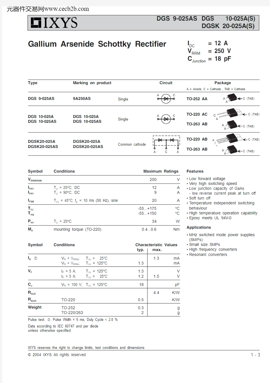
Type Marking on product
Circuit
Package
DGS 9-025AS 9A250AS
DGS 10-025A DGS 10-025A DGS 10-025AS DGS 10-025AS
DGSK20-025A DGSK20-025A DGSK20-025AS DGSK20-025AS
A = Anode, C = Cathode , TA
B = Cathode
A
TO-252 AA
A
I DC =12 A V RRM =250 V C Junction =18 pF
Gallium Arsenide Schottky Rectifier
Single
Common cathode
A C
A
C
Single Features
?Low forward voltage
?Very high switching speed ?Low junction capacity of GaAs
- low reverse current peak at turn off ?Soft turn off
?Temperature independent switching behaviour
?High temperature operation capability ?Epoxy meets UL 94V-0Applications
?MHz switched mode power supplies (SMPs)
?Small size SMPs
?High frequency converters ?Resonant converters
A
A TO-263 AB
A
A
TO-263 AB
TO-220 AB
A C A
C TO-220 AC A
C (TAB)
Symbol Conditions Maximum Ratings
V RRM/RSM 250
V I FAV T C = 25°C; DC 12A I FAV T C = 90°C; DC
9A I FSM T VJ = 45°C; t p = 10 ms (50 Hz), sine
20
A T VJ -55...+175°C T stg -55...+150
°C P tot T C = 25°C
34W M d
mounting torque (TO-220)
0.4...0.6
Nm
Pulse test: Pulse Width = 5 ms, Duty Cycle < 2.0 %Data according to IEC 60747 and per diode unless otherwise specified
Symbol Conditions
Characteristic Values typ.max.
I R V R = V RRM ;T VJ = 25°C 1.3
mA V R = V RRM ;T VJ = 125°C 1.3mA V F I F = 5 A;T VJ = 125°C 1.3V I F = 5 A;
T VJ = 25°C
1.2 1.5
V C J V R = 100 V;T VJ = 125°C
18
pF R thJC 4.4K/W R thCH TO-2200.5K/W Weight
TO-2520.3g TO-220/263
2
g
0435
IXYS reserves the right to change limits, test conditions and dimensions
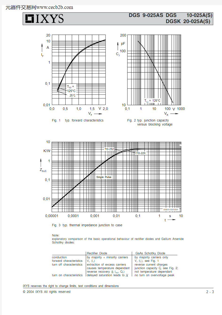
0,000010,00010,0010,010,11
10
t
s Fig. 3typ. thermal impedance junction to case
Note:
explanatory comparison of the basic operational behaviour of rectifier diodes and Gallium Arsenide Schottky diodes:
conduction
forward characteristics turn off characteristics
turn on characteristics
by majority + minority carriers V F (I F )
extraction of excess carriers causes temperature dependant reverse recovery (t rr , I RM , Q rr )delayed saturation leads to V FR Rectifier Diode
by majority carriers only V F (I F ), see Fig. 1
reverse current charges
junction capacity C J , see Fig. 2;not temperature dependant no turn on overvoltage peak
GaAs Schottky Diode
1 Anode
2 NC
3 Anode
4 Cathode