
This is information on a product in full production.
January 2015
DocID027114 Rev 21/88
11 timers, ADC, communication interfaces, 2.4 - 3.6 V
Datasheet - production data
Features
?Core: ARM ? 32-bit Cortex ?-M0 CPU, frequency up to 48 MHz ?Memories
–32 to 128 Kbytes of Flash memory
– 6 to 16 Kbytes of SRAM with HW parity ?CRC calculation unit
?Reset and power management
–Digital & I/Os supply: V DD = 2.4 V to 3.6 V –Analog supply: V DDA = V DD to 3.6 V
–Power-on/Power down reset (POR/PDR)–Low power modes: Sleep, Stop, Standby ?Clock management
– 4 to 32 MHz crystal oscillator
–32 kHz oscillator for RTC with calibration –Internal 8 MHz RC with x6 PLL option –Internal 40 kHz RC oscillator ?Up to 51 fast I/Os
–All mappable on external interrupt vectors –Up to 5155 I/Os with 5V tolerant capability ?5-channel DMA controller
?One 12-bit, 1.0 μs ADC (up to 16 channels)–Conversion range: 0 to 3.6 V
–Separate analog supply: 2.4 V to 3.6 V ?Calendar RTC with alarm and periodic wakeup from Stop/Standby ?11 timers
–One 16-bit advanced-control timer for six-channel PWM output
–Up to seven 16-bit timers, with up to four IC/OC, OCN, usable for IR control decoding
–Independent and system watchdog timers –SysTick timer
?Communication interfaces –Up to two I 2C interfaces –one supporting Fast Mode Plus
(1 Mbit/s) with 20 mA current sink,–one supporting SMBus/PMBus.–Up to four USARTs supporting master synchronous SPI and modem control; one with auto baud rate detection
–Up to two SPIs (18 Mbit/s) with 4 to 16 programmable bit frames
–USB 2.0 full-speed interface with BCD and LPM support ?Serial wire debug (SWD)
?All packages ECOPACK ?2
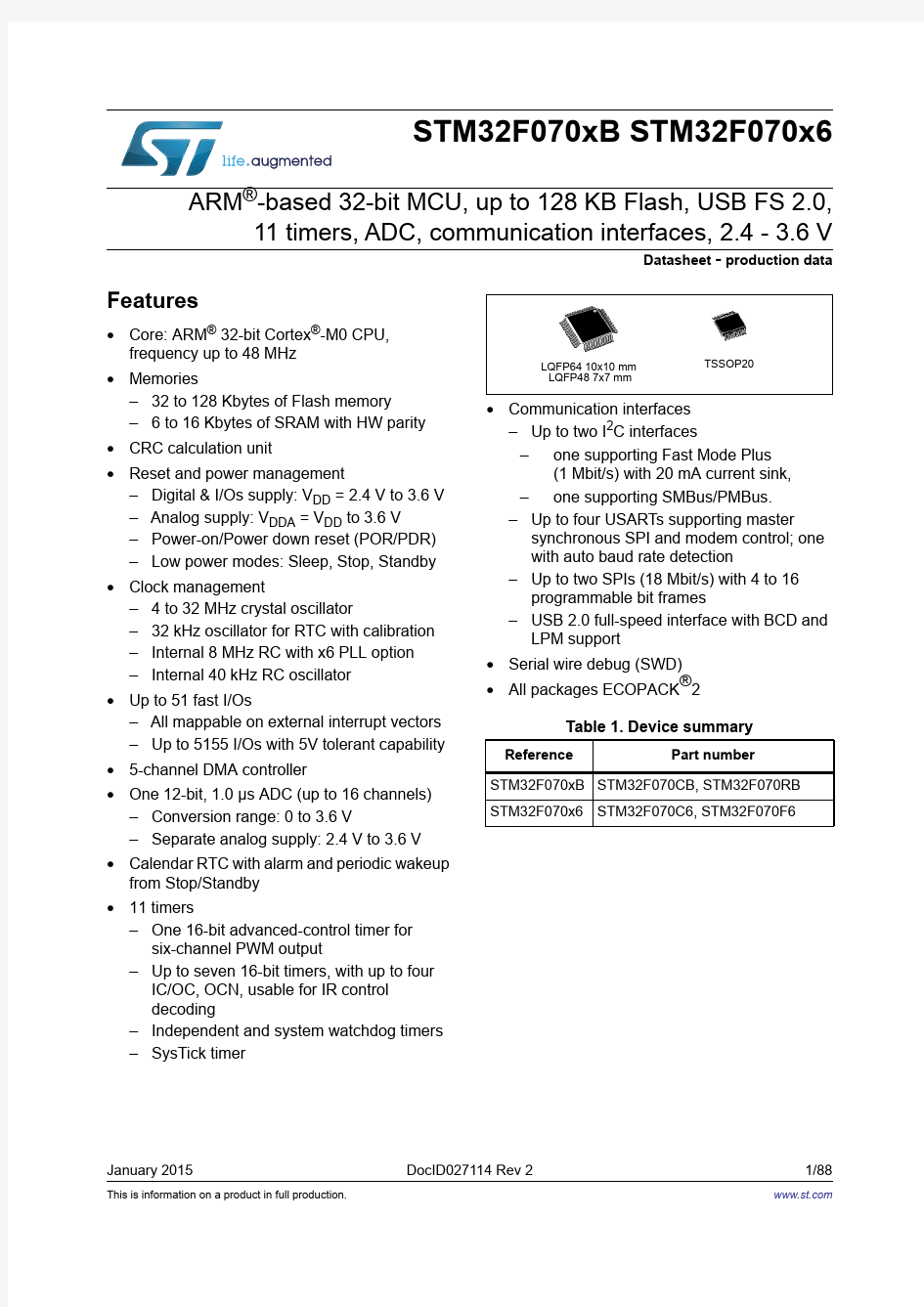
TSSOP20
https://www.doczj.com/doc/244747664.html,
Contents STM32F070xB STM32F070x6
Contents
1Introduction . . . . . . . . . . . . . . . . . . . . . . . . . . . . . . . . . . . . . . . . . . . . . . . . 8 2Description . . . . . . . . . . . . . . . . . . . . . . . . . . . . . . . . . . . . . . . . . . . . . . . . . 9
3Functional overview . . . . . . . . . . . . . . . . . . . . . . . . . . . . . . . . . . . . . . . . 12
3.1ARM?-Cortex?-M0 core with embedded Flash and SRAM . . . . . . . . . . . 12
3.2Memories . . . . . . . . . . . . . . . . . . . . . . . . . . . . . . . . . . . . . . . . . . . . . . . . . 12
3.3Boot modes . . . . . . . . . . . . . . . . . . . . . . . . . . . . . . . . . . . . . . . . . . . . . . . 12
3.4Cyclic redundancy check calculation unit (CRC) . . . . . . . . . . . . . . . . . . . 13
3.5Power management . . . . . . . . . . . . . . . . . . . . . . . . . . . . . . . . . . . . . . . . . 13
3.5.1Power supply schemes . . . . . . . . . . . . . . . . . . . . . . . . . . . . . . . . . . . . .13
3.5.2Power supply supervisors . . . . . . . . . . . . . . . . . . . . . . . . . . . . . . . . . . .13
3.5.3Voltage regulator . . . . . . . . . . . . . . . . . . . . . . . . . . . . . . . . . . . . . . . . . .13
3.5.4Low-power modes . . . . . . . . . . . . . . . . . . . . . . . . . . . . . . . . . . . . . . . . .14
3.6Clocks and startup . . . . . . . . . . . . . . . . . . . . . . . . . . . . . . . . . . . . . . . . . . 14
3.7General-purpose inputs/outputs (GPIOs) . . . . . . . . . . . . . . . . . . . . . . . . . 15
3.8Direct memory access controller (DMA) . . . . . . . . . . . . . . . . . . . . . . . . . . 16
3.9Interrupts and events . . . . . . . . . . . . . . . . . . . . . . . . . . . . . . . . . . . . . . . . 16
3.9.1Nested vectored interrupt controller (NVIC) . . . . . . . . . . . . . . . . . . . . . .16
3.9.2Extended interrupt/event controller (EXTI) . . . . . . . . . . . . . . . . . . . . . .16
3.10Analog to digital converter (ADC) . . . . . . . . . . . . . . . . . . . . . . . . . . . . . . . 17
3.10.1Temperature sensor . . . . . . . . . . . . . . . . . . . . . . . . . . . . . . . . . . . . . . . .17
3.10.2Internal voltage reference (V REFINT) . . . . . . . . . . . . . . . . . . . . . . . . . . .17
3.11Timers and watchdogs . . . . . . . . . . . . . . . . . . . . . . . . . . . . . . . . . . . . . . . 18
3.11.1Advanced-control timer (TIM1) . . . . . . . . . . . . . . . . . . . . . . . . . . . . . . .19
3.11.2General-purpose timers (TIM3, TIM1
4..17) . . . . . . . . . . . . . . . . . . . . . .19
3.11.3Basic timers TIM6 and TIM7 . . . . . . . . . . . . . . . . . . . . . . . . . . . . . . . . .20
3.11.4Independent watchdog (IWDG) . . . . . . . . . . . . . . . . . . . . . . . . . . . . . . .20
3.11.5System window watchdog (WWDG) . . . . . . . . . . . . . . . . . . . . . . . . . . .20
3.11.6SysTick timer . . . . . . . . . . . . . . . . . . . . . . . . . . . . . . . . . . . . . . . . . . . . .20
3.12Real-time clock (RTC) . . . . . . . . . . . . . . . . . . . . . . . . . . . . . . . . . . . . . . . 21
3.13Inter-integrated circuit interfaces (I2C) . . . . . . . . . . . . . . . . . . . . . . . . . . . 21
3.14Universal synchronous/asynchronous receiver transmitters (USART) . . 22
STM32F070xB STM32F070x6Contents
3.15Serial peripheral interface (SPI) . . . . . . . . . . . . . . . . . . . . . . . . . . . . . . . . 23
3.16Universal serial bus (USB) . . . . . . . . . . . . . . . . . . . . . . . . . . . . . . . . . . . . 23
3.17Serial wire debug port (SW-DP) . . . . . . . . . . . . . . . . . . . . . . . . . . . . . . . . 23
4Pinouts and pin descriptions . . . . . . . . . . . . . . . . . . . . . . . . . . . . . . . . . 24 5Memory mapping . . . . . . . . . . . . . . . . . . . . . . . . . . . . . . . . . . . . . . . . . . . 34
6Electrical characteristics . . . . . . . . . . . . . . . . . . . . . . . . . . . . . . . . . . . . 37
6.1Parameter conditions . . . . . . . . . . . . . . . . . . . . . . . . . . . . . . . . . . . . . . . . 37
6.1.1Minimum and maximum values . . . . . . . . . . . . . . . . . . . . . . . . . . . . . . .37
6.1.2Typical values . . . . . . . . . . . . . . . . . . . . . . . . . . . . . . . . . . . . . . . . . . . .37
6.1.3Typical curves . . . . . . . . . . . . . . . . . . . . . . . . . . . . . . . . . . . . . . . . . . . .37
6.1.4Loading capacitor . . . . . . . . . . . . . . . . . . . . . . . . . . . . . . . . . . . . . . . . .37
6.1.5Pin input voltage . . . . . . . . . . . . . . . . . . . . . . . . . . . . . . . . . . . . . . . . . .37
6.1.6Power supply scheme . . . . . . . . . . . . . . . . . . . . . . . . . . . . . . . . . . . . . .38
6.1.7Current consumption measurement . . . . . . . . . . . . . . . . . . . . . . . . . . .39
6.2Absolute maximum ratings . . . . . . . . . . . . . . . . . . . . . . . . . . . . . . . . . . . . 39
6.3Operating conditions . . . . . . . . . . . . . . . . . . . . . . . . . . . . . . . . . . . . . . . . 41
6.3.1General operating conditions . . . . . . . . . . . . . . . . . . . . . . . . . . . . . . . . .41
6.3.2Operating conditions at power-up / power-down . . . . . . . . . . . . . . . . . .41
6.3.3Embedded reset and power control block characteristics . . . . . . . . . . .42
6.3.4Embedded reference voltage . . . . . . . . . . . . . . . . . . . . . . . . . . . . . . . . .42
6.3.5Supply current characteristics . . . . . . . . . . . . . . . . . . . . . . . . . . . . . . . .42
6.3.6Wakeup time from low-power mode . . . . . . . . . . . . . . . . . . . . . . . . . . .48
6.3.7External clock source characteristics . . . . . . . . . . . . . . . . . . . . . . . . . . .49
6.3.8Internal clock source characteristics . . . . . . . . . . . . . . . . . . . . . . . . . . .55
6.3.9PLL characteristics . . . . . . . . . . . . . . . . . . . . . . . . . . . . . . . . . . . . . . . .56
6.3.10Memory characteristics . . . . . . . . . . . . . . . . . . . . . . . . . . . . . . . . . . . . .57
6.3.11EMC characteristics . . . . . . . . . . . . . . . . . . . . . . . . . . . . . . . . . . . . . . . .57
6.3.12Electrical sensitivity characteristics . . . . . . . . . . . . . . . . . . . . . . . . . . . .59
6.3.13I/O current injection characteristics . . . . . . . . . . . . . . . . . . . . . . . . . . . .60
6.3.14I/O port characteristics . . . . . . . . . . . . . . . . . . . . . . . . . . . . . . . . . . . . . .60
6.3.15NRST pin characteristics . . . . . . . . . . . . . . . . . . . . . . . . . . . . . . . . . . . .66
6.3.1612-bit ADC characteristics . . . . . . . . . . . . . . . . . . . . . . . . . . . . . . . . . . .68
6.3.17Temperature sensor characteristics . . . . . . . . . . . . . . . . . . . . . . . . . . . .71
6.3.18Timer characteristics . . . . . . . . . . . . . . . . . . . . . . . . . . . . . . . . . . . . . . .71
Contents STM32F070xB STM32F070x6
6.3.19Communication interfaces . . . . . . . . . . . . . . . . . . . . . . . . . . . . . . . . . . .72
7Package characteristics . . . . . . . . . . . . . . . . . . . . . . . . . . . . . . . . . . . . . 76
7.1Package mechanical data . . . . . . . . . . . . . . . . . . . . . . . . . . . . . . . . . . . . 76
7.2Thermal characteristics . . . . . . . . . . . . . . . . . . . . . . . . . . . . . . . . . . . . . . 85
7.2.1Reference document . . . . . . . . . . . . . . . . . . . . . . . . . . . . . . . . . . . . . . .85 8Part numbering . . . . . . . . . . . . . . . . . . . . . . . . . . . . . . . . . . . . . . . . . . . . 86 9Revision history . . . . . . . . . . . . . . . . . . . . . . . . . . . . . . . . . . . . . . . . . . . 87
STM32F070xB STM32F070x6List of tables List of tables
Table 1.Device summary. . . . . . . . . . . . . . . . . . . . . . . . . . . . . . . . . . . . . . . . . . . . . . . . . . . . . . . . . .1 Table 2.STM32F070xB/6 family device features and peripheral counts . . . . . . . . . . . . . . . . . . . . .10 Table 3.Temperature sensor calibration values. . . . . . . . . . . . . . . . . . . . . . . . . . . . . . . . . . . . . . . .17 Table 4.Internal voltage reference calibration values . . . . . . . . . . . . . . . . . . . . . . . . . . . . . . . . . . .17 Table 5.Timer feature comparison. . . . . . . . . . . . . . . . . . . . . . . . . . . . . . . . . . . . . . . . . . . . . . . . . .18 Table https://www.doczj.com/doc/244747664.html,parison of I2C analog and digital filters. . . . . . . . . . . . . . . . . . . . . . . . . . . . . . . . . . . .21 Table 7.STM32F070xB/6 I2C implementation. . . . . . . . . . . . . . . . . . . . . . . . . . . . . . . . . . . . . . . . .22 Table 8.STM32F070xB/6 USART implementationF070 . . . . . . . . . . . . . . . . . . . . . . . . . . . . . . . . .22 Table 9.STM32F070xB/6 SPI implementation. . . . . . . . . . . . . . . . . . . . . . . . . . . . . . . . . . . . . . . . .23 Table 10.Legend/abbreviations used in the pinout table. . . . . . . . . . . . . . . . . . . . . . . . . . . . . . . . . .26 Table 11.STM32F070xB/6 pin definitions . . . . . . . . . . . . . . . . . . . . . . . . . . . . . . . . . . . . . . . . . . . . .26 Table 12.Alternate functions selected through GPIOA_AFR registers for port A . . . . . . . . . . . . . . .31 Table 13.Alternate functions selected through GPIOB_AFR registers for port B . . . . . . . . . . . . . . .32 Table 14.Alternate functions selected through GPIOC_AFR registers for port C . . . . . . . . . . . . . . .33 Table 15.Alternate functions selected through GPIOD_AFR registers for port D . . . . . . . . . . . . . . .33 Table 16.Alternate functions selected through GPIOF_AFR registers for port F. . . . . . . . . . . . . . . .33 Table 17.STM32F070xB/6 peripheral register boundary addresses. . . . . . . . . . . . . . . . . . . . . . . . .35 Table 18.Voltage characteristics . . . . . . . . . . . . . . . . . . . . . . . . . . . . . . . . . . . . . . . . . . . . . . . . . . . .39 Table 19.Current characteristics . . . . . . . . . . . . . . . . . . . . . . . . . . . . . . . . . . . . . . . . . . . . . . . . . . . .40 Table 20.Thermal characteristics. . . . . . . . . . . . . . . . . . . . . . . . . . . . . . . . . . . . . . . . . . . . . . . . . . . .40 Table 21.General operating conditions . . . . . . . . . . . . . . . . . . . . . . . . . . . . . . . . . . . . . . . . . . . . . . .41 Table 22.Operating conditions at power-up / power-down . . . . . . . . . . . . . . . . . . . . . . . . . . . . . . . .41 Table 23.Embedded reset and power control block characteristics. . . . . . . . . . . . . . . . . . . . . . . . . .42 Table 24.Embedded internal reference voltage. . . . . . . . . . . . . . . . . . . . . . . . . . . . . . . . . . . . . . . . .42 Table 25.Typical and maximum current consumption from V DD supply at V DD = 3.6 V . . . . . . . . . .43 Table 26.Typical and maximum current consumption from the V DDA supply . . . . . . . . . . . . . . . . . .44 Table 27.Typical and maximum consumption in Stop and Standby modes . . . . . . . . . . . . . . . . . . .44 Table 28.Typical current consumption in Run mode, code with data processing
running from Flash. . . . . . . . . . . . . . . . . . . . . . . . . . . . . . . . . . . . . . . . . . . . . . . . . . . . . . .45 Table 29.Switching output I/O current consumption . . . . . . . . . . . . . . . . . . . . . . . . . . . . . . . . . . . . .47 Table 30.Low-power mode wakeup timings. . . . . . . . . . . . . . . . . . . . . . . . . . . . . . . . . . . . . . . . . . . .48 Table 31.High-speed external user clock characteristics. . . . . . . . . . . . . . . . . . . . . . . . . . . . . . . . . .49 Table 32.Low-speed external user clock characteristics. . . . . . . . . . . . . . . . . . . . . . . . . . . . . . . . . .50 Table 33.HSE oscillator characteristics. . . . . . . . . . . . . . . . . . . . . . . . . . . . . . . . . . . . . . . . . . . . . . .51 Table 34.LSE oscillator characteristics (f LSE = 32.768 kHz) . . . . . . . . . . . . . . . . . . . . . . . . . . . . . . .53 Table 35.HSI oscillator characteristics. . . . . . . . . . . . . . . . . . . . . . . . . . . . . . . . . . . . . . . . . . . . . . . .55 Table 36.HSI14 oscillator characteristics. . . . . . . . . . . . . . . . . . . . . . . . . . . . . . . . . . . . . . . . . . . . . .55 Table 37.LSI oscillator characteristics. . . . . . . . . . . . . . . . . . . . . . . . . . . . . . . . . . . . . . . . . . . . . . . .56 Table 38.PLL characteristics . . . . . . . . . . . . . . . . . . . . . . . . . . . . . . . . . . . . . . . . . . . . . . . . . . . . . . .56 Table 39.Flash memory characteristics. . . . . . . . . . . . . . . . . . . . . . . . . . . . . . . . . . . . . . . . . . . . . . .57 Table 40.Flash memory endurance and data retention. . . . . . . . . . . . . . . . . . . . . . . . . . . . . . . . . . .57 Table 41.EMS characteristics . . . . . . . . . . . . . . . . . . . . . . . . . . . . . . . . . . . . . . . . . . . . . . . . . . . . . .58 Table 42.EMI characteristics . . . . . . . . . . . . . . . . . . . . . . . . . . . . . . . . . . . . . . . . . . . . . . . . . . . . . . .58 Table 43.ESD absolute maximum ratings . . . . . . . . . . . . . . . . . . . . . . . . . . . . . . . . . . . . . . . . . . . . .59 Table 44.Electrical sensitivities . . . . . . . . . . . . . . . . . . . . . . . . . . . . . . . . . . . . . . . . . . . . . . . . . . . . .59 Table 45.I/O current injection susceptibility. . . . . . . . . . . . . . . . . . . . . . . . . . . . . . . . . . . . . . . . . . . .60 Table 46.I/O static characteristics . . . . . . . . . . . . . . . . . . . . . . . . . . . . . . . . . . . . . . . . . . . . . . . . . . .61 Table 47.Output voltage characteristics. . . . . . . . . . . . . . . . . . . . . . . . . . . . . . . . . . . . . . . . . . . . . . .64
List of tables STM32F070xB STM32F070x6 Table 48.I/O AC characteristics. . . . . . . . . . . . . . . . . . . . . . . . . . . . . . . . . . . . . . . . . . . . . . . . . . . . .65 Table 49.NRST pin characteristics . . . . . . . . . . . . . . . . . . . . . . . . . . . . . . . . . . . . . . . . . . . . . . . . . .66 Table 50.ADC characteristics . . . . . . . . . . . . . . . . . . . . . . . . . . . . . . . . . . . . . . . . . . . . . . . . . . . . . .68 Table 51.R AIN max for f ADC = 14 MHz. . . . . . . . . . . . . . . . . . . . . . . . . . . . . . . . . . . . . . . . . . . . . . . .69 Table 52.ADC accuracy. . . . . . . . . . . . . . . . . . . . . . . . . . . . . . . . . . . . . . . . . . . . . . . . . . . . . . . . . . .69 Table 53.TS characteristics. . . . . . . . . . . . . . . . . . . . . . . . . . . . . . . . . . . . . . . . . . . . . . . . . . . . . . . .71 Table 54.TIMx characteristics . . . . . . . . . . . . . . . . . . . . . . . . . . . . . . . . . . . . . . . . . . . . . . . . . . . . . .71 Table 55.IWDG min/max timeout period at 40 kHz (LSI). . . . . . . . . . . . . . . . . . . . . . . . . . . . . . . . . .72 Table 56.WWDG min/max timeout value at 48 MHz (PCLK). . . . . . . . . . . . . . . . . . . . . . . . . . . . . . .72 Table 57.I2C analog filter characteristics. . . . . . . . . . . . . . . . . . . . . . . . . . . . . . . . . . . . . . . . . . . . . .73 Table 58.SPI characteristics . . . . . . . . . . . . . . . . . . . . . . . . . . . . . . . . . . . . . . . . . . . . . . . . . . . . . . .73 Table https://www.doczj.com/doc/244747664.html,B electrical characteristics. . . . . . . . . . . . . . . . . . . . . . . . . . . . . . . . . . . . . . . . . . . . . . .75 Table 60.LQFP64 - 10 x 10 mm low-profile quad flat package mechanical data. . . . . . . . . . . . . . . .77 Table 61.LQFP48 - 7mm x 7mm low-profile quad flat package mechanical data . . . . . . . . . . . . . .80 Table 62.TSSOP20 - 20-pin thin shrink small outline package mechanical data . . . . . . . . . . . . . . .83 Table 63.Package thermal characteristics. . . . . . . . . . . . . . . . . . . . . . . . . . . . . . . . . . . . . . . . . . . . .85 Table 64.Ordering information scheme . . . . . . . . . . . . . . . . . . . . . . . . . . . . . . . . . . . . . . . . . . . . . . .86 Table 65.Document revision history. . . . . . . . . . . . . . . . . . . . . . . . . . . . . . . . . . . . . . . . . . . . . . . . . .87
STM32F070xB STM32F070x6List of figures List of figures
Figure 1.Block diagram. . . . . . . . . . . . . . . . . . . . . . . . . . . . . . . . . . . . . . . . . . . . . . . . . . . . . . . . . . .11 Figure 2.Clock tree . . . . . . . . . . . . . . . . . . . . . . . . . . . . . . . . . . . . . . . . . . . . . . . . . . . . . . . . . . . . . .15 Figure 3.LQFP64 64-pin package pinout (top view) . . . . . . . . . . . . . . . . . . . . . . . . . . . . . . . . . . . . .24 Figure 4.LQFP48 48-pin package pinout (top view) . . . . . . . . . . . . . . . . . . . . . . . . . . . . . . . . . . . . .25 Figure 5.TSSOP20 20-pin package pinout (top view). . . . . . . . . . . . . . . . . . . . . . . . . . . . . . . . . . . .25 Figure 6.STM32F070xB/6 memory map. . . . . . . . . . . . . . . . . . . . . . . . . . . . . . . . . . . . . . . . . . . . . .34 Figure 7.Pin loading conditions. . . . . . . . . . . . . . . . . . . . . . . . . . . . . . . . . . . . . . . . . . . . . . . . . . . . .37 Figure 8.Pin input voltage. . . . . . . . . . . . . . . . . . . . . . . . . . . . . . . . . . . . . . . . . . . . . . . . . . . . . . . . .37 Figure 9.Power supply scheme. . . . . . . . . . . . . . . . . . . . . . . . . . . . . . . . . . . . . . . . . . . . . . . . . . . . .38 Figure 10.Current consumption measurement scheme . . . . . . . . . . . . . . . . . . . . . . . . . . . . . . . . . . .39 Figure 11.High-speed external clock source AC timing diagram . . . . . . . . . . . . . . . . . . . . . . . . . . . .49 Figure 12.Low-speed external clock source AC timing diagram. . . . . . . . . . . . . . . . . . . . . . . . . . . . .50 Figure 13.Typical application with an 8 MHz crystal. . . . . . . . . . . . . . . . . . . . . . . . . . . . . . . . . . . . . .52 Figure 14.Typical application with a 32.768 kHz crystal. . . . . . . . . . . . . . . . . . . . . . . . . . . . . . . . . . .54 Figure 15.TC and TTa I/O input characteristics . . . . . . . . . . . . . . . . . . . . . . . . . . . . . . . . . . . . . . . . .62 Figure 16.Five volt tolerant (FT and FTf) I/O input characteristics . . . . . . . . . . . . . . . . . . . . . . . . . . .63 Figure 17.I/O AC characteristics definition . . . . . . . . . . . . . . . . . . . . . . . . . . . . . . . . . . . . . . . . . . . . .66 Figure 18.Recommended NRST pin protection . . . . . . . . . . . . . . . . . . . . . . . . . . . . . . . . . . . . . . . . .67 Figure 19.ADC accuracy characteristics. . . . . . . . . . . . . . . . . . . . . . . . . . . . . . . . . . . . . . . . . . . . . . .70 Figure 20.Typical connection diagram using the ADC . . . . . . . . . . . . . . . . . . . . . . . . . . . . . . . . . . . .70 Figure 21.SPI timing diagram - slave mode and CPHA = 0 . . . . . . . . . . . . . . . . . . . . . . . . . . . . . . . .74 Figure 22.SPI timing diagram - slave mode and CPHA = 1 . . . . . . . . . . . . . . . . . . . . . . . . . . . . . . . .74 Figure 23.SPI timing diagram - master mode. . . . . . . . . . . . . . . . . . . . . . . . . . . . . . . . . . . . . . . . . . .75 Figure 24.LQFP64 - 10 x 10 mm 64 pin low-profile quad flat package outline. . . . . . . . . . . . . . . . . .77 Figure 25.LQFP64 recommended footprint. . . . . . . . . . . . . . . . . . . . . . . . . . . . . . . . . . . . . . . . . . . . .78 Figure 26.LQFP64 marking example (package top view). . . . . . . . . . . . . . . . . . . . . . . . . . . . . . . . . .79 Figure 27.LQFP48 - 7mm x 7mm, 48 pin low-profile quad flat package outline. . . . . . . . . . . . . . . .80 Figure 28.LQFP48 recommended footprint. . . . . . . . . . . . . . . . . . . . . . . . . . . . . . . . . . . . . . . . . . . . .81 Figure 29.LQFP48 marking example (package top view). . . . . . . . . . . . . . . . . . . . . . . . . . . . . . . . . .82 Figure 30.TSSOP20 - 20-pin thin shrink small outline . . . . . . . . . . . . . . . . . . . . . . . . . . . . . . . . . . . .83 Figure 31.TSSOP20 recommended footprint . . . . . . . . . . . . . . . . . . . . . . . . . . . . . . . . . . . . . . . . . . .84 Figure 32.TSSOP20 marking example (package top view) . . . . . . . . . . . . . . . . . . . . . . . . . . . . . . . .84
Introduction STM32F070xB STM32F070x6
1 Introduction
This datasheet provides the ordering information and mechanical device characteristics of the STM32F070xB/6 microcontrollers.
This document should be read in conjunction with the STM32F0x0xx reference manual (RM0360). The reference manual is available from the STMicroelectronics website https://www.doczj.com/doc/244747664.html, .
For information on the ARM ? Cortex
?-M0 core, please refer to the Cortex ?-M0 Technical Reference Manual, available from the https://www.doczj.com/doc/244747664.html, website.
STM32F070xB STM32F070x6Description 2 Description
The STM32F070xB/6 microcontrollers incorporate the high-performance ARM? Cortex?-
M0 32-bit RISC core operating at a 48 MHz frequency, high-speed embedded memories (up
to 128 Kbytes of Flash memory and up to 16 Kbytes of SRAM), and an extensive range of
enhanced peripherals and I/Os. All devices offer standard communication interfaces (up to
two I2Cs, up to two SPIs and up to four USARTs), one USB Full speed device, one 12-bit
ADC, seven general-purpose 16-bit timers and an advanced-control PWM timer.
The STM32F070xB/6 microcontrollers operate in the -40 to +85 °C temperature range from
a 2.4 to 3.6V power supply. A comprehensive set of power-saving modes allows the design
of low-power applications.
The STM32F070xB/6 microcontrollers include devices in three different packages ranging
from 20 pins to 64 pins. Depending on the device chosen, different sets of peripherals are
included. The description below provides an overview of the complete range of
STM32F070xB/6 peripherals proposed.
These features make the STM32F070xB/6 microcontrollers suitable for a wide range of
applications such as application control and user interfaces, handheld equipment, A/V
receivers and digital TV, PC peripherals, gaming and GPS platforms, industrial applications,
PLCs, inverters, printers, scanners, alarm systems, video intercoms, and HVACs.
Description STM32F070xB STM32F070x6
STM32F070xB STM32F070x6Description
Functional overview STM32F070xB STM32F070x6
3 Functional overview
3.1 ARM ?-Cortex ?-M0 core with embedded Flash and SRAM
The ARM ? Cortex ?-M0 processor is the latest generation of ARM processors for
embedded systems. It has been developed to provide a low-cost platform that meets the needs of MCU implementation, with a reduced pin count and low-power consumption, while delivering outstanding computational performance and an advanced system response to interrupts.
The ARM ? Cortex ?-M0 32-bit RISC processor features exceptional code-efficiency, delivering the high-performance expected from an ARM core in the memory size usually associated with 8- and 16-bit devices.
The STM32F0xx family has an embedded ARM core and is therefore compatible with all ARM tools and software.
Figure 1 shows the general block diagram of the device family.
3.2 Memories
The device has the following features:? 6 to 16 Kbytes of embedded SRAM accessed (read/write) at CPU clock speed with 0
wait states and featuring embedded parity checking with exception generation for fail-critical applications.?The non-volatile memory is divided into two arrays:
–32 to 128 Kbytes of embedded Flash memory for programs and data –Option bytes
The option bytes are used to write-protect the memory (with 4 KB granularity) and/or readout-protect the whole memory with the following options:–Level 0: no readout protection –Level 1: memory readout protection, the Flash memory cannot be read from or
written to if either debug features are connected or boot in RAM is selected
–Level 2: chip readout protection, debug features (Cortex ?-M0 serial wire) and
boot in RAM selection disabled
3.3 Boot modes
At startup, the boot pin and boot selector option bit are used to select one of the three boot
options:?Boot from User Flash ?Boot from System Memory ?Boot from embedded SRAM The boot loader is located in System Memory. It is used to reprogram the Flash memory by using USART on pins PA14/PA15 or PA9/PA10.
STM32F070xB STM32F070x6Functional overview
3.4 Cyclic redundancy check calculation unit (CRC)
The CRC (cyclic redundancy check) calculation unit is used to get a CRC code using a
configurable generator polynomial value and size.
Among other applications, CRC-based techniques are used to verify data transmission or
storage integrity. In the scope of the EN/IEC 60335-1 standard, they offer a means of
verifying the Flash memory integrity. The CRC calculation unit helps compute a signature of
the software during runtime, to be compared with a reference signature generated at link-
time and stored at a given memory location.
management
3.5 Power
3.5.1 Power supply schemes
?V DD = 2.4 to 3.6V: external power supply for I/Os and the internal regulator. Provided externally through V DD pins.
?V DDA = from V DD to 3.6V: external analog power supply for ADC, Reset blocks, RCs and PLL (minimum voltage to be applied to V DDA is 2.4 V when the ADC is used). The
V DDA voltage level must be always greater or equal to the V DD voltage level and must
be provided first.
For more details on how to connect power pins, refer to Figure9: Power supply scheme.
3.5.2 Power supply supervisors
The device has integrated power-on reset (POR) and power-down reset (PDR) circuits.
They are always active, and ensure proper operation above a threshold of 2 V. The device
remains in reset mode when the monitored supply voltage is below a specified threshold,
V POR/PDR, without the need for an external reset circuit.
?The POR monitors only the V DD supply voltage. During the startup phase it is required that V DDA should arrive first and be greater than or equal to V DD.
?The PDR monitors both the V DD and V DDA supply voltages, however the V DDA power supply supervisor can be disabled (by programming a dedicated Option bit) to reduce
the power consumption if the application design ensures that V DDA is higher than or
equal to V DD.
3.5.3 Voltage
regulator
The regulator has two operating modes and it is always enabled after reset.
?Main (MR) is used in normal operating mode (Run).
?Low power (LPR) can be used in Stop mode where the power demand is reduced.
In Standby mode, it is put in power down mode. In this mode, the regulator output is in high
impedance and the kernel circuitry is powered down, inducing zero consumption (but the
contents of the registers and SRAM are lost).
Functional overview STM32F070xB STM32F070x6
3.5.4 Low-power modes
The STM32F070xB/6 microcontrollers support three low-power modes to achieve the best
compromise between low power consumption, short startup time and available wakeup sources:?Sleep mode
In Sleep mode, only the CPU is stopped. All peripherals continue to operate and can wake up the CPU when an interrupt/event occurs.?Stop mode
Stop mode achieves very low power consumption while retaining the content of SRAM and registers. All clocks in the 1.8 V domain are stopped, the PLL, the HSI RC and the HSE crystal oscillators are disabled. The voltage regulator can also be put either in normal or in low power mode.
The device can be woken up from Stop mode by any of the EXTI lines. The EXTI line source can be one of the 16 external lines and RTC.?Standby mode
The Standby mode is used to achieve the lowest power consumption. The internal voltage regulator is switched off so that the entire 1.8 V domain is powered off. The PLL, the HSI RC and the HSE crystal oscillators are also switched off. After entering Standby mode, SRAM and register contents are lost except for registers in the RTC domain and Standby circuitry.
The device exits Standby mode when an external reset (NRST pin), an IWDG reset, a rising edge on the WKUP pins, or an RTC event occurs.
Note:
The RTC, the IWDG, and the corresponding clock sources are not stopped by entering Stop or Standby mode.
3.6 Clocks and startup
System clock selection is performed on startup, however the internal RC 8 MHz oscillator is selected as default CPU clock on reset. An external 4-32 MHz clock can be selected, in which case it is monitored for failure. If failure is detected, the system automatically switches back to the internal RC oscillator. A software interrupt is generated if enabled. Similarly, full interrupt management of the PLL clock entry is available when necessary (for example on failure of an indirectly used external crystal, resonator or oscillator).
Several prescalers allow the application to configure the frequency of the AHB and the APB domains. The maximum frequency of the AHB and the APB domains is 48 MHz.
STM32F070xB STM32F070x6Functional overview
3.7 General-purpose inputs/outputs (GPIOs)
Each of the GPIO pins can be configured by software as output (push-pull or open-drain), as
input (with or without pull-up or pull-down) or as peripheral alternate function. Most of the
GPIO pins are shared with digital or analog alternate functions.
The I/O configuration can be locked if needed following a specific sequence in order to
avoid spurious writing to the I/Os registers.
Functional overview STM32F070xB STM32F070x6
3.8 Direct memory access controller (DMA)
The 5-channel general-purpose DMA manages memory-to-memory, peripheral-to-memory and memory-to-peripheral transfers.
The DMA supports circular buffer management, removing the need for user code intervention when the controller reaches the end of the buffer.
Each channel is connected to dedicated hardware DMA requests, with support for software trigger on each channel. Configuration is made by software and transfer sizes between source and destination are independent.
The DMA can be used with the main peripherals: SPI, I2C, USART, all TIMx timers (except TIM14) and ADC.
3.9
Interrupts and events
3.9.1
Nested vectored interrupt controller (NVIC)
The STM32F0xx family embeds a nested vectored interrupt controller able to handle up to
32 maskable interrupt channels (not including the 16 interrupt lines of Cortex ?
-M0) and 4 priority levels.?Closely coupled NVIC gives low latency interrupt processing ?Interrupt entry vector table address passed directly to the core ?Closely coupled NVIC core interface ?Allows early processing of interrupts ?Processing of late arriving higher priority interrupts ?Support for tail-chaining ?Processor state automatically saved ?Interrupt entry restored on interrupt exit with no instruction overhead This hardware block provides flexible interrupt management features with minimal interrupt latency.
3.9.2 Extended interrupt/event controller (EXTI)
The extended interrupt/event controller consists of 32 edge detector lines used to generate interrupt/event requests and wake-up the system. Each line can be independently
configured to select the trigger event (rising edge, falling edge, both) and can be masked independently. A pending register maintains the status of the interrupt requests. The EXTI can detect an external line with a pulse width shorter than the internal clock period. Up to 51 GPIOs can be connected to the 16 external interrupt lines.
STM32F070xB STM32F070x6Functional overview
3.10 Analog to digital converter (ADC)
The 12-bit analog to digital converter has up to 16 external and two internal (temperature
sensor, voltage reference measurement) channels and performs conversions in single-shot
or scan modes. In scan mode, automatic conversion is performed on a selected group of
analog inputs.
The ADC can be served by the DMA controller.
An analog watchdog feature allows very precise monitoring of the converted voltage of one,
some or all selected channels. An interrupt is generated when the converted voltage is
outside the programmed thresholds.
sensor
3.10.1 Temperature
The temperature sensor (TS) generates a voltage V SENSE that varies linearly with
temperature.
The temperature sensor is internally connected to the ADC_IN16 input channel which is
used to convert the sensor output voltage into a digital value.
The sensor provides good linearity but it has to be calibrated to obtain good overall
accuracy of the temperature measurement. As the offset of the temperature sensor varies
from chip to chip due to process variation, the uncalibrated internal temperature sensor is
suitable for applications that detect temperature changes only.
To improve the accuracy of the temperature sensor measurement, each device is
individually factory-calibrated by ST. The temperature sensor factory calibration data are
stored by ST in the system memory area, accessible in read-only mode.
3.10.2 Internal voltage reference (V REFINT)
The internal voltage reference (V REFINT) provides a stable (bandgap) voltage output for the
ADC. V REFINT is internally connected to the ADC_IN17 input channel. The precise voltage
of V REFINT is individually measured for each part by ST during production test and stored in
the system memory area. It is accessible in read-only mode.
Functional overview STM32F070xB STM32F070x6
3.11 Timers and watchdogs
The STM32F070xB/6 devices include up to six general-purpose timers, two basic timers
and one advanced control timer.
Table5 compares the features of the different timers.
1.Not available on STM32F070x6 devices.
STM32F070xB STM32F070x6Functional overview
3.11.1 Advanced-control timer (TIM1)
The advanced-control timer (TIM1) can be seen as a three-phase PWM multiplexed on six
channels. It has complementary PWM outputs with programmable inserted dead times. It
can also be seen as a complete general-purpose timer. The four independent channels can
be used for:
?Input capture
?Output compare
?PWM generation (edge or center-aligned modes)
?One-pulse mode output
If configured as a standard 16-bit timer, it has the same features as the TIMx timer. If
configured as the 16-bit PWM generator, it has full modulation capability (0-100%).
The counter can be frozen in debug mode.
Many features are shared with those of the standard timers which have the same
architecture. The advanced control timer can therefore work together with the other timers
via the Timer Link feature for synchronization or event chaining.
3.11.2 General-purpose timers (TIM3, TIM1
4..17)
There are five synchronizable general-purpose timers embedded in the STM32F070xB/6
devices (see Table5 for differences). Each general-purpose timer can be used to generate
PWM outputs, or as simple time base.
TIM3
STM32F070xB/6 devices feature one synchronizable 4-channel general-purpose timer.
TIM3 is based on a 16-bit auto-reload up/downcounter and a 16-bit prescaler. It features
four independent channels each for input capture/output compare, PWM or one-pulse mode
output. This gives up to 12 input captures/output compares/PWMs on the largest packages.
The TIM3 general-purpose timer can work with the TIM1 advanced-control timer via the
Timer Link feature for synchronization or event chaining.
TIM3 has an independent DMA request generation.
This timer is capable of handling quadrature (incremental) encoder signals and the digital
outputs from 1 to 3 hall-effect sensors.
The counter can be frozen in debug mode.
TIM14
This timer is based on a 16-bit auto-reload upcounter and a 16-bit prescaler.
TIM14 features one single channel for input capture/output compare, PWM or one-pulse
mode output.
Its counter can be frozen in debug mode.
TIM15, TIM16 and TIM17
These timers are based on a 16-bit auto-reload upcounter and a 16-bit prescaler.
TIM15 has two independent channels, whereas TIM16 and TIM17 feature one single
channel for input capture/output compare, PWM or one-pulse mode output.
Functional overview STM32F070xB STM32F070x6
The TIM15, TIM16 and TIM17 timers can work together, and TIM15 can also operate withTIM1 via the Timer Link feature for synchronization or event chaining.TIM15 can be synchronized with TIM16 and TIM17.
TIM15, TIM16 and TIM17 have a complementary output with dead-time generation and independent DMA request generation.Their counters can be frozen in debug mode.
3.11.3 Basic timers TIM6 and TIM7
These timers can be used as a generic 16-bit time base.
3.11.4 Independent watchdog (IWDG)
The independent watchdog is based on an 8-bit prescaler and 12-bit downcounter with user-defined refresh window. It is clocked from an independent 40 kHz internal RC and as it operates independently from the main clock, it can operate in Stop and Standby modes. It can be used either as a watchdog to reset the device when a problem occurs, or as a free running timer for application timeout management. It is hardware or software configurable through the option bytes. The counter can be frozen in debug mode.
3.11.5 System window watchdog (WWDG)
The system window watchdog is based on a 7-bit downcounter that can be set as free running. It can be used as a watchdog to reset the device when a problem occurs. It is clocked from the APB clock (PCLK). It has an early warning interrupt capability and the counter can be frozen in debug mode.
3.11.6 SysTick timer
This timer is dedicated to real-time operating systems, but could also be used as a standard
down counter. It features:? A 24-bit down counter ?Autoreload capability ?Maskable system interrupt generation when the counter reaches 0?Programmable clock source (HCLK or HCLK/8)