Differential Amplifiers
- 格式:pdf
- 大小:440.28 KB
- 文档页数:30

射频共模抗扰度英文English:"Radiofrequency common mode rejection, often abbreviated as RF CMRR, refers to the ability of a system or device to reject unwanted signals or interference that appear simultaneously on both signal lines or conductors. It is a crucial parameter in electronic systems, especially in communication and instrumentation applications, where signal integrity is essential. RF CMRR is typically expressed in decibels (dB) and is calculated as the ratio of the desired signal to the unwanted common-mode signal. Higher RF CMRR values indicate better rejection of common-mode interference, leading to improved performance and reliability of the system. Achieving high RF CMRR involves various design techniques, including proper grounding, shielding, and balanced signal routing, as well as the use of differential amplifiers and filters to attenuate common-mode signals. Moreover, careful attention to component selection and layout plays a significant role in optimizing RF CMRR. Overall, RF CMRR is a fundamental aspect of ensuring the accurate transmission and reception of radiofrequency signals while minimizing interference and noise."中文翻译:"射频共模抗扰度,通常简称为RF CMRR,指的是系统或设备拒绝同时出现在信号线或导体上的不需要的信号或干扰的能力。


English | 日本語亚洲技术支持中心中文技术支持所有位置放大器专区讨论
4 回复最新回复: 2014-1-21 下午5:54 作者 ADIForum
ADIForum 2013-11-28 上午11:22
工程师百问百答——放大、电平搬移和驱动精密系
统
放大器是数据采集和传输系统的主要器件。
它们采集并放大来自传感器
和变送器的低电平信号,可从高噪声和高共模电压水平的环境下提取出
这些信号。
此外,放大器可以改变信号范围,并实现单端-差分转换(或
差分-单端转换),以便完全匹配ADC的输入范围。
ADI在线设计峰会2013,在10月底举办了“放大、电平搬移和驱动精密
系统”的主题研讨会,会后咱们的专家,放大器应用工程师David对大
家各种问题给出了详细的解答,我们选出了其中具有代表性的问题,整
理分享给大家。
关于更多“ADI在线设计峰会2013”相关内容,请点
击
生
喜爱 (0)
ADIForum2014-1-21 下午5:54 (回复 ADIForum)
Re: 工程师百问百答——放大、电平搬移和驱动精密系统
此次会议的演讲PPT资料,请见附件
放大器----信号调理和精密系统驱动.pdf(4.4 MB) 预
览
喜爱 (0)
职业联络ADI关于ADI投资信息新闻中心关于网站网站地图E nglish日本語电子新闻快讯
© 1995 - 2013 Analog Devices, Inc. All Rights Reserved。

16Date of Issue WORLDSKILLS QUALITY ASSURANCE STANDARD Document No.TD16 Approved Technical Description – Industrial Electronics Revision1WorldSkills (International Vocational Training Organisation), by a resolution of the Technical Committee and in accordance with the Constitution, the Standing Orders and the Competition Rules, has adopted the following minimum requirements for trade No. 16 for the WorldSkills Competition:The effective date will be that date on which this document is issued, subject to approval by the Chairman of the Technical Committee.1Name and description of trade1.1The name of the trade is:Industrial Electronics1.2The Industrial Electronics Technician works in industrial or commercialenvironments and works with or studies electronics. This includes:- development- construction- design- measuring- testing- repair1.3This technical description must be known to every candidate.1.4In the event of any query or conflict within the technical descriptions, the Englishcopy will take precedence1.5Words implying masculine gender only shall include the feminine gender2Scope of work at WorldSkills Competitions2.1The practical work will test the competitors ability to:- assemble, adjust, commission, measure and test electronic equipment- carry out and document measurements on analogue and digital circuits- locate, document and repair faults in a given circuit- design or refine a design of a circuit, and construct using prototypeconstruction techniques2.2To solve theoretical tasks using mathematical and graphical methods to aTechnician Level2.3To redraw a circuit drawing schematic with Computer Aided Design.Competitors must bring their own laptop and software of their choice.3Competition Format for Practical Work3.1AssemblingAssemble a project that has to be from a kit of parts to the IPC-A-610 issue Cinternational acceptability of electronic assemblies. (Web page/main/ipca/htm. Each project should be able to fit a Euro cardstandard using DIN 41612 F64 or F32connectors, that will fit a standard backplane connector. Power points will be as follows: -A1C1+5v DigitalA2C2Digital GroundA15+5v AnalogC15+12v AnalogA16C16Analog groundA17-5v AnalogC17-12v AnalogA31C31Digital GroundA32C32+5v Digital3.2Measuring and TestingTo work with conventional measuring and testing equipment for AC, DC, digitaland analog electronics. To test, set, adjust and measure electronic components,modules and equipment. To record and analyse measured results. Boards willbe pre-built before the competition.3.3Fault Finding and RepairTo test, locate and replace faulty electronic components on a printed circuitboard, surface mount board or mixed technology board.All surface mountcomponents to have no more than four pins and Fault finding method/procedurewith results will be required. All boards will be pre-built before the competition.Each board will have at least three faults. Pin configurations and power supplywill be as 3.0.Competitors may bring their own measurement instruments.3.4Prototype DesignTo carry out a simple electronic design using given components to meet a givenspecification. Printed circuit boards should be pre-built. Resistors E24 series,0.25 watt to be available from host country.No more than 15 wire wrapconnections and no more 15 point to point connections will be required on thismodule. Pin configurations and power supply will be as 3.0.Competitors may bring their own measurement instruments.3.5The competition is modular and will be marked at the end of every module.3.6Time allowed for each module is as follows:Theory 2 hoursDrawing 2 hoursPrototype 4 hoursFault Finding 4 hoursMeasurement 4 hoursAssembly Project 3 + 3 hours4Theoretical Knowledge4.1To solve theoretical problems, using mathematical and graphical methods basedon the following:4.1.1Fundamental electronic principles:1. Basics of AC and DC technology.2. Two ports LRC networks, resistive networks with up to three meshes.3. RC oscillators.4.1.2Components in Electronics:Properties, behaviour, characteristics and application (elementary circuits) ofmechanically, electrically and physically adjustable components i.e.:-Resistors-Capacitors-Coils-Transformers-Diodes: rectifying diodes, switch diodes, zener diodes, capacitive diodes, PIN diodes-Trigger components: diac, triac, thyristor and uni-junction transistors.4.1.3Multistage and special amplifier circuits:Basic amplifier circuits (AC, DC and power amplifiers)Differential amplifiers/operational amplifiers.1. Ideal operational amplifier: (infinite input resistance, zero outputresistance and infinite open loop grain) Basic circuits with operationalamplifier, analogue adder and subtractor, differentiator, comparator,impedance transducer.2. Real operational amplifier: Offset voltage and offset current,compensation, common mode gain and rejection, temperature drift,frequency response.4.1.4Generators and Pulse shapers:1. Generators for sine wave voltage: RC, quartz, LC oscillator; wien bridgegenerator, phase generator.2. Pulse shaper: Schmitt trigger, differentiator, integrator.4.1.5Digital Electronics1. Basic logic gates.2. Level switching function, function table, pulse, diagram, circuit symbols(table in appendix).3. Properties of basic gates AND, OR, NOT, NAND, NOR, EXCLUSIVE OREXCLUSIVE NOR.4. Substituting basic NAND or NOR gates for basic gates.5. Creating switching functions from given circuits and vice versa.6. Making function table from circuit diagrams and switching functions.7. Simplifying switching networks using Karnaugh diagram or mathematicaltechniques.8. Flip-flops; RS Flip-flop, D Flip-flop, JK Master slave Flip-flop (especiallycounter circuits, shift register and frequency divider).9. Memory circuits, selection, addressing, and memory decoding volume.5Materials5.1ComponentsThe workshop master must ensure that the materials provided are completed,packed in bags and checked also for the power supply project, and range of E24,0.25w resistors from 10 ohm to 10 megohms is supplied. The host country willalso supply the back plane as per drawing –Refer Document 4.3/PD16 – Project Design Criteria5.2Other materials1. Graph paper A3 size2. Solder 60/40 type3. Approx. 5m bare wire (0.5mm diameter) per competitor4. Approx. 5m each of insulated wire (or standard wire) in five differentcolours for each competitor5. Binding/insulation tape6. Lacing string /Tie raps/heat shrink sleeving7. Hot-air fan for heat-shrink tubing5.5ClothingWork clothes must comply with relevant safety standards. Safety standardsrequire a minimum of safety glasses and covered footwear.6Workshop Installations6.1The working area should provide enough space for the competitors, experts(jury), measurement and repair area, material cupboards and wardrobes.6.2The general layout of the workshop venue will be as below, with sufficient spacefor the booth and for the competitors working area as defined in 6.3 below.Key to the layout above is:Please note that this is an example of the layout, and is not definitive. The minimum area requirements will be available.6.2.1General RequirementsThe working area should provide enough space for the competitors, expert’s (jury), measurement and repair area, material cupboards and wardrobes.Lockable cupboards must be provided for the safe keeping of the materials and the examination papers under the responsibility of the chief expert.The organizers will provide four sets of the following for the experts:1. 4 x Hot-air fan for heat-shrink tubing2. 2 x Magnifiers for experts x3 or x53. 2 x Computers4. One Laser printer6.3The personal working area for each competitor should be about 3m x 3m, andshall also allow for the equipment and machines specified in Sec. 6.4 below.6.4Measuring Instruments and Tester/ToolsThe organisers will provide the following for each competitor:1. 1x universal DVM2. 1x Function generator 1-50 MHz, sine, square, triangle3. 1x stabilized power supply (3-30V adjustable)4. Various connection cables (if necessary, coax cable with BNC plugs)5. 1x Bench Lamp6. 1x Electrostatic workstation7. 1x Calculator, non-progammableThe organizers will also provide a spare set of the above for the experts.6.5Competitors must bring all their own tools, including wire-wrapping equipment.Measurement instruments are optional.Each competitor may send his tools ahead to the host country in a light, sturdy and lockable toolbox. A complete list of the contents must accompany the toolbox for Customs clearance i6.5.1Unauthorised tools are not permitted. In case of doubt, the competitor must applyto the Jury in advance. Their decision will take into consideration technological progress and the aim of the competition.7Test Project Marking7.1The experts will decide together on the test projects, the marking criteria and thedimensional tolerances on forms 5, and 6, and they will prepare the marking list.Any Country who has a project submitted and his/her candidate gains a largerscore and all the other competitors have a low score, the average of all the lowscores will be awarded to the country competitor who submitted the project.7.2Marks:Perfect = 10 pointsVery good = 9 pointsGood = 8 pointsRather good = 7pointsSufficient = 6 pointsMedium = 5 pointsWeak = 4 pointsInsufficient = 3 pointsVery bad = 2 pointsZero = 1 point7.3RatingSection Item Maximum PointsA Theory10B Drawing10C Prototype22D Fault Finding22E Measurement22F Assembly Project15GH7.4Conversion to the 400 - 600 scale will be done by computer.8Competition Procedure8.1The competition will be worked on over all four days of the competition. Moduleswill be completed on each day for all competitors so that progressive markingcan take place, and for results to be made available each day.8.2Competitors will have time made available to familiarise themselves with materialand processes. Where processes are particularly difficult, the host country willprovide a subject matter expert to demonstrate the process and the competitorswill be given the opportunity to practice.8.3The competitors will be given all competition documents including the markingcriteria one hour prior to the commencement of the competition so that they maystudy the requirements8.4Prior to the start of the competition, each competitor will receive a detailedtimetable reflecting the timing for completion of modules.8.5Project Design, Selection and Documentation will be carried out as specified inAppendix 1PCB information is provided in Appendix 68.6Ballot Selection of Competitors Work Areas, Competition Notes and Timetable8.6.1For a total random selection procedure, the country codes should be placed inone bin and workbench numbers in another. Alphabetically the countrycompetitors will select one piece of paper from each, and this is then the startbench for that country.8.7The rules and procedures, and timetable specified in Appendix 2, 3 and 4 mustbe complied with.9Judging procedural requirements9.1The experts that attend the competition will be divided into marking groups todeal with each section of the marking criteria.9.2Every completed module will be marked on the same day in which it wascompleted.10General safety requirements10.1All competitors must use safety glasses when using any hand, power or machinetools or equipment likely to cause or create chips or fragments that may injurethe eyes10.2All competitors must wear appropriate clothing.10.3All machinery, equipment and safety clothing must comply with the safety rulesof the organising country.10.4Competitors must keep their workspace clear of obstacles and the floor spaceclean of material and equipment - any items likely to cause the competitor to trip,slip or fall.10.5Failure by the competitor to comply with safety directions or instructions mayincur penalties for safety.10.8Judges will wear the appropriate personal safety equipment when inspecting,checking or otherwise working with a competitor’s project.10.9Safety Checklist must be adhered to and is provided in Appendix 511Additional Documentation11.1The following additional documentation relates to this trade.•Nil at present11.2The following additional documentation relating to this trade has yet to be definedat the next WorldSkills Competition to be held in St Gallen in 2003.•Document TM16 – Trade Management Procedures•Document WS16 – Workshop Setup•Document PD16 – Project Design CriteriaTrade 16 Electronics - Competition ManagementThe following Countries will provide the following at the 2003 competition.Country AssemblyProject MeasuringandTestingFaultFindingandRepairDesign/PrototypeTheory1 Digital1AnalogDrawingBrazil X XCanada X X X Finland X X X Germany X X XJapan X X X Korea X X X Macao XLit X X XMorocco X X Portugal X X X X Singapore X X X Switzerland X XTaiwan x X X Tunisia x x XUnitedKingdomx x x x Project Selection GuidelinesAll competition presentations will be made in English and before any project is presented for selection they must be checked that they conform to the current rules of the world skills, and the current Technical Description. If the rules are not followed the project will not be considered for selection. All documentation must adhere to the world skills rules otherwise it will not be selected. The experts will form into a project group with other countries under the same heading. They will then select either one or a number of projects for the competition, as for the timetable as 3:7. Experts will then present their selection to the rest of the experts. Following everyone’s approval the experts will then agree a marking scheme for the project/ projects. When the competition begins, these experts manage and mark that aspect of the competition under guidance from the Chief Expert.Project DocumentationProject documentation must be brought to the competition on 3.5” floppy disc format,/CD in Microsoft Word. Where experts have used a drawing software. Experts should bring along the version of the drawing program software that they used. Paper copies should also be presented and where possible in three official languages. Where possible circuit diagrams will be used for all modules and project wording should be as brief as possible. All projects must include the following:-1. Short project brief2. Parts list3. Circuit diagram4. Data sheet pack5. Projects will only be accepted with softwareFirst Time CountriesAny Countries attending the competition for the first time should contact the Chief Expert via world skills who will then forward previous competition documentation and agree a project in advance for consideration.Competition Rules for Competitors while working on their Projects1. You must not talk to your own country expert or visitor without the presence of one other expert2. If you have a question raise your hand.3. You must not leave your workstation without permission, except to obtain wire etc from centrebench.4. If you feel ill or require anything, raise your hand.5. You may not leave the stand without an escort except at scheduled times for lunch and visitsto other stands.6. You must not touch any project other than your own.7. You may not touch any other competitors equipment.8. If you finish and leave your stand early, you must leave the stand.9. No use of mobile phones is permitted.10. No talking to any people outside the stand area while you are working on a project.Competition Timetable - Trade 16 Industrial ElectronicsDay 1Step Activity Start time Finish time 1Introduction by Chief judge9.009.159.1509.452Demonstration of assembly rack andpower supplies3Start assembly10.0013.00 4Lunch13.0014.00 5Continue with assembly of project14.0017.00 Total competition time 6.00 Day 2Step Activity Start time Finish time 1Drawing Introduction9.009.30 2Drawing/C programming9.3011.30 3Tour around venue and lunch11.3012.00 4Theory Introduction12.4513.00 5Theory13.0015.00 6Break15.0015.15 7Demonstration of Fault Finding one project15.1515.30 8Fault finding one15.3017.30 Total competition time 6.00 Day 3Step Activity Start time Finish time 1Introduction to Design Project9.0009.30 2Design & prototype09.3012.30 3Lunch12.3014.00 4Demonstration of fault finding project14.0014.15number 25Fault finding14.1516.15 6Tour around venue16.1517.00 Total competition time 5.00 Day 4Step Activity Start time Finish time9.009.151Demonstration of Measurement andTesting project2Measurement project9.1512.15 3Lunch12.1513.30 4Demonstration of C programming project13.3014.005 C programming project14.0016.00 Total competition time 5.00 Overall competition time22.00FAIRNESSAs part of World Skills each competition is required to have a fairness of competition rules for the experts, which are listed below for your comments.Before the competition startsAll experts are to be trustedExperts to believe in each other and their valuesEffective management of timeCommunicate both accurate and completeKeep communication with team members user-friendlyBe a good listenerAs a team we value the contributions of its membersReach early agreement and our goals and have contingency plansCreate a vision of success for other competitions to followWe will not make preformed judgementsRecognise issues early and open dialogue then explore for common groundIf you have a visitor to the stand he/she must not speak to the competitorsBe united in our decisionsAlways show a united front when dealing with the competitorsWhen the competitors arriveYou must not talk to your own country competitor or visitor without the presence of one otherexpertYou must not leave the stand when your competitor is away from the stand unless in the presenceof another expertNo use of mobile phones is permitted.Health and Safety Check ListList each item A to C'A' = Satisfactory'B' = Unsatisfactory but rectified immediately'C' = Unsatisfactory - remedial action required1.Are all exits from the area free of obstruction?2.Are all gangways within the area free from obstruction?3.Are all fire fighting appliances at their designated, location, and access to them notobstructed?4.Do Experts / Competitors in the area know:a) Means of escape in emergency.b) The location of fire equipment and alarm points.c) What action to take if the evacuation alarm sounds.d) The action to take if a person is seriously ill / injured.5.Is the floor surface safe?6.Are items of furniture in a sound condition e.g. lockers, tables, chairs, benches etc.7.Are cables and extension leads on electrical equipment, at the plug?8.Are electrical wall sockets secure and in good condition.9.Are the following satisfactory:a) Lightingb) Ventilationc) Temperatured) Noise levele) Extraction10.Are "fittings" in a safe state, e.g. lights, service supplies etc.11.Are all items of handling equipment in a safe condition, e.g. trolleys etc. and up to date.(In the area)?15Are all filing cabinet drawers functioning correctly, and are drawers prevented from coming out by limit stops.16Are metal cabinets free from sharp edges.17Are the tops of units free from unsuitable objects.18Is there suitable storage provided (and used) for cabinet drawer locking bars, when not in use.19If applicable, are paper guillotines properly guarded.20Does the area demonstrate a satisfactory level of decent house-keeping? e.g. steps, ladders etc. (are they in good condition)?22Are heavy items stored on low level racks.24Are all personnel trained to use appropriate equipment in this area (see supervision)25Are there necessary restrictions being enforced e.g. entry of unauthorised persons.26Are flammable liquids and chemicals stored in appropriate environment correctly, e.g.gloves, goggles etc?28Are the edges of areas marked with a hazard stripe.29Are all equipment that require guarding, fitted with secure are serviceable guards?30Is eye protection being worn in appropriate areas.32Are there other items of safety equipment avqilable for use.33Are tools in good condition.34Are all raw materials or equipment safely positioned.35Is there a list of authorised persons who may use machines or equipment?36Are waste materials correctly disposed of?37If chemicals or substances are used, are they in suitable containers that are correctly marked?38Is safety information for chemicals or substances used available and known to the user?39Are the emergency stop buttons on equipment assessable and clearly marked?41Are competitors supervised.42Are free standing gas bottles secured.43Are all tools in use in good condition.44Are free standing gas bottles secure.45If applicable, have all system components been subjected to test, is a certificate available?46If applicable, is equipment within validation.47If applicable, is pipe work adequately secured.48Are there written procedures for :-a) Setting up for test.b) Test procedure.c) Making safe after test.50Are the necessary restrictions being enforced e.g. entry of unauthorised personnel. 51Do all personnel know the main isolation controls of the services being used?52Are cables and flexible hoses correctly routed to prevent accidents or damage?53If flammable liquids or chemicals are being use, are they :-a) Of minimal quantity.b) In approved containers.c) Correctly labelled.54Have reasonable safety precautions been taken against any foreseeable occurrence whilst carrying out the test.55If applicable, is the equipment correctly bonded / earthed.56If competitors or others are working in the area, are they under full supervision. Chief Expert (Signature)....................................................APPENDIX 6Specifications for PCB cardsMechanical spec.’sThe Europe format for PCB card is specified as follow (PCB only):All Dimensions are in millimeters. Tc = 160 mmThe Europe format for PCB card with a front plateIs specified as follow (with front plate and DIN41612 connector):All Dimensions are in millimeters. Tc = 160 mmFront Plate dimensions (if needed): 40,64 mm x 128,7 mm x 2,5 mmPCB connectorEach card must be designed with a DIN41612 male 64 pins a + c (C form)connector for PCB. The reference from HARTING is: 0903.164.6921.Mechanical dimensions of the connector。
为了测量电阻,我们使用单位“欧姆”。
To measure resistance,we use the unit "ohm".重要的是要应用这些定律。
It is important to apply these laws. 这种装置能用来测量电流电压电阻。
Such a device can be used to measurecurrent,voltage and resistance. 我们想要求这个电流中的电流。
We wish to find the current in the circuit.无线电波的用途之一是发送信息。
One of the uses of radio waves is to transmit intelligence.在这种情况下该物体被说成带电了。
In this case the object is said to be charged.我们感到理解这个概念很困难。
We find it very difficult to understand this concept.工科学生应该知道如何使用计算机。
Engineering studentsshould know how to use acomputer.物体做工的能力被称为能量。
The ability of a body to do workis called energy.重要的是我们要把理论应用于实践。
It is important for us toapply theory to practice.计算在这个电流中流动的电流密度是可能的。
It is possible tocalculate the current flowing inthis circuit.这些是常用的设备。
These arecommonly used devices.电压等取决于电路中的电阻以及所加的电压。
Voltage equalscurrent multiplied byresistance.显然电流与外加电压成正比。
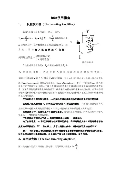
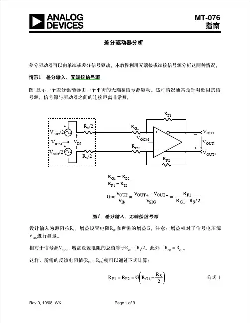
运放使用指南1、反相放大器(The Inverting Amplifier )基本反相放大器电路如图1所示。
其中,i V R R V ⨯-=12o ,213||R R R =,当12R R 的数值远小于op 开环增益时,这个数值就是反相放大器的增益,运算放大器的输入阻抗就是1R 的值,闭环增益单位增益带宽闭环增益带宽+=1在设计时要注意的是:3R 的阻值应该等于1R 和2R 的并联阻值,以减小输入偏置电流所带来的失调电压。
闭环增益输入失调电压输出失调电压⨯=。
运放输入端失调电压的主要来源是偏置电流(Input bias current )和输入失调电压(Input offest voltage )。
对于一个给定的op ,输入失调电压就已经确定了,但是由于输入失调电流所带来的失调电压与所采用的电路的结构有关系。
为了在不使用使调整电路的情况下,减小输入偏置电流所带来的失调电压,应该使得同相输入端和反相输入端对地直流电阻相等,使得由于偏置电流在输入电阻上压降所带来的失调电压相互抵消。
在低内阻信号源的放大器中,op 的输入失调电压将成为失调电压误差的主要来源。
在高输入阻抗的情况下,失调电压可以采用3R 的阻值来调整,利用输入偏置电流在其上的压降来对输入失调电压做补偿(即用这个得到的压降来抵消输入失调电压)。
在交流耦合时,失调电压并不显得很重要。
这时的主要问题是:失调电压减小了输入电压峰——峰值的线性动态范围。
工作范围在闭环状态下的op 和其反馈网络的增益——频率特性为了实现稳定,op 和反馈环路对任何频率的信号,在环路增益大于1时的环路相移的角度绝对不能超过o180。
在实践上,为了达到稳定条件,相移角度不应该接近o180。
对于一个给定的op 放大器电路,在进行电容补偿是需要在稳定性和带宽之间进行权衡。
加大补偿电容可以提高稳定性。
但是牺牲了放大器的增益带宽,反之亦然。
2、同相放大器(The Non-Inverting Amplifier )图2是高输入阻抗的同相放大器电路,其闭环放大倍数121R R +=, V io图1 反相放大器其3dB 带宽闭环增益单位增益带宽=。
共模反馈笔记Return To Innocence咳咳,为了坚持更新,贴一篇以前对全差分运放的共模反馈的小结..关于全差分放大器对于全差分放大器,一般可以得到更大的swing (由于差分信号),同时可以实现对共模干扰、噪声以及偶数阶的非线性的抑制;但其需要有两个匹配的反馈网络,以及共模反馈电路顺便提一下,对于全差分的折叠共源共栅(folded cascode)放大器,需要注意转换速率(正向与负向)对输入对差分对的尾电流源和cascode电流源的考虑非主极点的位置–输入对管的drain节点(注意全差分没有镜像极点的问题..),如果考虑PMOS输入的结构,将会折叠到n管的cascode,从而减小此节点阻抗,提高此非主极点的频率;但是P输入结构亦有其问题,如直流增益和cmfb电路的速度(考虑cmfb控制的为cascode的pmos电流源)关于共模反馈CMFB从反馈环路来看,共模的稳定问题来源于闭环的共模增益:由于输入差分对的尾电流源的local-feedback,通常共模增益较小,导致运放无法控制其输出共模点;通过CMFB共模反馈电路,可以提高共模反馈环路的增益,以稳定共模信号。
设计CMFB需考虑补偿以减小环路的稳定时间(settling time)和提高稳定性。
从性能上,我们希望共模反馈的单位增益带宽足够大,但由于cmfb的环路相较于差模通路可能有更多高频极点,故此在一定的功耗要求下其UGB一般比较难做的高,有书中提到可以将其设计为差模UGB 的1/3一般共模反馈的方法是控制放大器的电流源,这里如果是folded-cascode的结构,可以考虑用cmfb控制cascode的电流源而不是输入差分对的电流源—-因其在共模环路中有较少的节点–>更容易补偿等..(另一种考虑是控制尾电流源可能导致共模增益的问题)另外,对于cmfb控制的尾电流源,常见将尾电流源分为两半,其中之一由cmfb控制,另一半接恒定偏置电流;这种结构的具体分析可见Gray书12.4.2节的内容,简单来说,single-stage的opamp中控制尾电流源的cmfb结构,其UGB 主要为gmt/CL, 其中gmt为尾电流源的跨导,这里拆分尾电流源来减半cmc共模控制的部分,这样UGB减小,即缩减带宽来提升共模反馈环路的相位裕度,当然cmfb的增益相应也减小了;另外恒定偏置部分也可帮助共模电压的初始建立,减小cmfb大的扰动。
运放差分放大器工作原理Op amps are widely used in electronic circuits for their ability to amplify signals with high accuracy and low distortion. 运算放大器在电子电路中被广泛使用,因为它们具有高精度和低失真的信号放大能力。
One common application of op amps is in differential amplifiers, which are used to amplify the voltage difference between two input signals. 差分放大器是运放的一种常见应用,用于放大两个输入信号之间的电压差。
By amplifying this voltage difference, the differential amplifier provides a way to amplify small signals while rejecting common-mode noise. 通过放大这种电压差,差分放大器提供了一种放大小信号并抑制共模噪声的方法。
The differential amplifier consists of two input terminals, labeled as inverting and non-inverting, and one output terminal. 差分放大器由两个输入端和一个输出端组成,分别标记为反相输入和非反相输入。
The inverting input is connected to one input signal, while the non-inverting input is connected to the other input signal. 反相输入连接到一个输入信号,而非反相输入连接到另一个输入信号。
常用电子技术词汇中英文对照表AAC equivalent circuit 交流等效电路AC load line 交流负载线Acceptor Impurity 受主杂质Active filter 有源滤波器Active load circuit 有源负载电路Active load 有源负载Active region 放大区Admittance 导纳Amplification factor 放大倍数Amplifier circuit 放大器电路Amplifier frequency response 放大器频率响应(频率特性) Amplifier 放大器Analog Circuit 模拟电路Analog Electronics 模拟电子(技术)Analog signal 模拟信号Anti-log amplifier 反对数(指数)放大器Attenuation 衰减Avalanche breakdown 雪崩击穿BBand-pass filter 带通滤波器Band-reject filter 带阻滤波器Bandwidth extension 频带展宽Bandwidth 带宽Base 基极Base-collector junction 集电结Base-emitter junction 发射结Basic FET differential pair 场效应管基本差分电路B-C junction 集电结Beta cutoff frequency 截止频率Bias circuit 偏置电路Bias stability 偏置稳定性Bias stable circuit 偏置稳定电路Biasing 偏置Bipolar amplifier 双极型放大器Bipolar circuit 双极型电路Bipolar junction transistor 双极型结型晶体三极管Bipolar linear amplifier 双极型线性放大器Bipolar operational amplifier circuit 双极型运算放大器Bipolar transistor biasing 双极型晶体管偏置Bipolar transistor current source 双极型电流源Bipolar transistor 双极型三极管Bi-stable multi-vibrator 多谐振荡器BJT amplifier 双极型放大器BJT circuit 双极型电路BJT diff-amps 双极型差分放大器BJT differential pair amplifier 晶体管差分放大器BJT operational amplifier circuit 双极型运算放大电路BJT power transistor 双极型功率晶体管Bode plot 波特图Body effect 衬底效应Breakdown effect 击穿效应Breakdown voltage 击穿电压Breakpoint frequency 转折频率Bridge circuit 桥式电路Bridge power amplifier 桥式功率放大器Bridge rectifier circuit 桥式整流电路Bridge rectifier 桥式整流器Buffer transistor 缓冲三极管Built-in potential barrier 内建势垒Butterworth filter 巴特沃斯滤波器Bypass capacitor 旁路电容CCarbon resistor 碳膜电阻Carriers 载流子Cascade current source 级联型电流源(串联型) Cascaded circuit 级联电路(串级电路) Cascode circuit mirror 共基共射(共栅共源)镜像电路Cascode circuits 共基共射(共栅共源)电路Cascode configuration 共基共射(共栅共源)组态Cascode current-mirror 共基共射(共栅共源)镜像电流源Channel length modulation 沟道长度调制Circuit biasing 电路偏置Circuit configuration 电路组态(结构)Circuit design 电路设计Circuit element matching 电路器件匹配Circuit gain 电路增益Circuit load line 电路负载线Circuit symbols and conventions 电路符号和惯例Circuit with active load 有源负载电路Clamper circuit 钳位电路Class A power amplifiers 甲类功率放大器(电路)Class AB biasing using the V BE multiplier 利用V BE倍增电路的甲乙类偏置Class AB output stage utilizing the Darlington configuration 达林顿结构的甲乙类输出级Class AB output stage with diode biasing 二极管偏置的甲乙类输出级Class AB output stage with input buffer transistors 带输入缓冲晶体管的甲乙类输出级Class AB output stage 甲乙类输出级(电路)Class AB power amplifiers 甲乙类功率放大器(电路)Class B power amplifiers 乙类功率放大器(电路)Class C power amplifiers 丙类功率放大器(电路)Clipper circuit 限幅电路Closed-loop frequency response 闭环频率响应Closed-loop gain 闭环增益Closed-loop transfer function 闭环传递函数Closed-loop voltage gain 闭环电压增益CMOS operational amplifier circuit CMOS运算放大器电路CMOS transmission gate CMOS传输门CMOS(complementary MOS) inverter CMOS(互补MOS)反相器Collector current 集电极电流Collector 集电极Common base amplifiers 共基放大器(电路)Common base characteristics 共基特性Common base circuit 共基电路Common base configuration 共基组态(结构)Common base current gain 共基电流增益Common bipolar circuit 常用双极型电路Common collector amplifiers 共集电极放大器(电路)Common collector configuration 共集电极组态(结构)Common emitter amplifiers 共射放大器(电路)Common emitter circuit 共射电路Common emitter configuration 共射组态(结构)Common gate circuit 共栅电路Common gate configuration 共栅组态(结构)Common mode 共模Common source amplifier 共源放大器(电路)Common source circuit 共源电路Common-gate configuration 共栅结构(共栅组态、共栅接法)Common-mode gain 共模增益Common-mode input impedance 共模输入阻抗Common-mode input resistance 共模输入电阻Common-mode input signal 共模输入信号Common-mode input voltage 共模输入电压Common-mode rejection ratio(CMRR)共模抑制比Comparator circuit 比较器电路Complex frequencies 复频率Computer simulation 计算机仿真COMS inverters CMOS反相器Concentrations 浓度Conductance 电导Conductivity 传导率Constant current source 恒流源Constant current 恒电流Conversion efficiency 转换效率Conversion factors 转换系数Converters 转换器、变换器Corner frequency 拐点频率Coupling capacitors 耦合电容Covalent bond 共价键Crossover distortion 交越失真Crystal oscillator (石英)晶体振荡器Current density 电流密度Current to voltage converters 电流/电压转换器Current voltage characteristics 电流电压特性Current voltage properties 电流电压特性Current voltage relationship 电流电压关系Cut-in voltage 开启电压Cutoff frequency 截止频率Cutoff 截止DDarlington pair configuration 达林顿结构DC analysis 直流分析DC isolation 直流隔离DC quantities 直流量DC transfer characteristics 直流传输特性Dead band 死区Decade frequency 十倍频Depletion load 耗尽型负载Depletion mode 耗尽型Depletion region 耗尽区Diff-amp frequency response 差分放大器频率响应Difference amplifier 差分放大器Differential amplifiers with active load 有源负载差分放大器Differential amplifiers 差分放大器Differential input signal 差模输入信号Differential input voltage 差模输入电压Differential mode input impedance 差模输入阻抗Differential mode input resistance 差模输入电阻Differential mode 差模Differential pair amplifiers 差分放大器Differential-mode input signal 差模输入信号Differentiators 微分器Diffusion capacitance 扩散电容Diffusion conductance 扩散电导Diffusion current 扩散电流Diffusion resistance 扩散电阻Diffusion 扩散Diffusion 扩散Diode breakdown 二极管击穿Diode circuit 二极管电路Discrete circuit representation 分立电路表达Discrete semiconductor devices 分立半导体器件Dissipation 耗散Distortion 失真Dominant pole 主极点Donor atoms 施主原子Donor impurity doping 施主杂质掺杂Donor impurity 施主杂质Doped semiconductors 掺杂半导体Doping 掺杂Drain current 漏极电流Drain terminal 漏极端子Drift current 飘移电流Drift velocity 飘移速度Drift 飘移Duty cycle 占空比EEarly effect 厄尔利效应Early voltage 厄尔利电压Electric field 电场Electrical vehicles 电动车Electron concentration 电子浓度Electron current 电子电流Electron inversion layer 电子反型层Electron mobility 电子迁移率Electron-hole recombination 电子-空穴复合Electronic devices 电子器件Emitter degeneration resistor 发射极电阻Emitter follower amplifier 射极跟随器放大器Emitter follower 射极跟随器Enhancement mode 增强模式Enhancement-load 增强型负载Equilibrium PN junction 动态平衡PN结Expanded hybrid π equivalent circuits 扩展混合π型等效电路Exponential amplifiers 指数放大器Extrinsic semiconductors 非本征半导体FFeedback amplifier 反馈放大器Feedback resistor 反馈电阻Feedback stability 反馈稳定性Feedback transfer function 反馈传递函数FET current source 场效应管电流源FET differential pair amplifier 场效应管差分放大器Field effect transistor 场效应管Filter capacitor 滤波电容Finite gain 有限增益Finite open-loop gain 有限开环增益First-order function 一阶函数Forward bias 正向偏置Forward diode resistance 反向二极管电阻Forward-bias voltage 正向偏置电压Forward-bias 正向偏置Forward-biased PN junction 正向偏置PN结Four-pole low-pass butterworth filter 四极低通巴特沃斯滤波器Frequency analysis 频率分析Frequency compensation 频率补偿Frequency response 频率响应Frequency-selective network 选频网络Full-power bandwidth 全功率带宽Full-wave rectification 全波整流GGain margins 增益裕度Gain sensitivity 增益灵敏度Gain stage 增益级Gain-bandwidth product 增益带宽积Gallium arsenide 砷化镓Gate terminal 栅极端子Germanium atoms 锗原子Graphical analysis 图解分析法HHalf-wave rectification 半波整流Harmonic distortion 谐波失真Heat sinks 散热片High frequency amplifiers 高频放大器High frequency equivalent circuit 高频等效电路Higher-order butterworth filters 高阶巴特沃斯滤波器High-frequency response 高频响应High-pass butterworth filter 高通巴特沃斯滤波器High-pass filter 高通滤波器High-pass network 高通网络Hole concentration 空穴浓度Hole drift velocity 空穴漂移速度Hole inversion layer 空穴反型层Hole mobility 空穴迁移率Holes 空穴H-parameters H参数Hybrid-π equivalent circuits 混合π型等效电路IIdeal closed loop gain 理想闭环增益Ideal feedback topologies 理想反馈拓扑(结构) Ideal topologies 理想拓扑(结构) Ideal voltage reference circuit 理想电压基准电路Impurity atoms 杂质原子Inductively coupled amplifiers 感性耦合放大器Inductively coupled power amplifiers 感性耦合功率放大器Input and output voltage limitations 输入输出电压限制Input bias current 输入偏置电流Input buffer transistors 输入缓冲晶体管Input diff-amp 输入差分放大器Input impedance 输入阻抗Input offset current 输入失调电流Input offset voltage 输入失调电压Input resistance 输入电阻Input stage 输入级Instantaneous values 瞬时值Instrumentation amplifier 仪用放大器Insulators 绝缘体Integrated circuit biasing 集成电路偏置Integrated circuit power amplifier 集成电路功率放大器Integrated circuit 集成电路Integrator and differentiator 积分器与微分器Integrators 积分器Intrinsic semiconductor 本征半导体Inverting amplifier 反相放大器Inverting input terminal 反相输入端Inverting Schmitt trigger 反相施密特触发器Inverting summing amplifier 反相求和放大器Iteration techniques 叠代法(递归法)JJFET amplifier 结型场效应管放大器JFET current source 结型场效应管电流源JFET operational amplifier 结型场效应管运算放大器Junction capacitance 结电容Junction field effect transistor 结型场效应管KKirchhoff's voltage law 基尔霍夫电压定律Kinetic theory 分子运动论Kirchhoff's current law 基尔霍夫电流定律LLeakage current 漏电流Line load 线路负载Line regulation 线路(电压)调整率Linear amplifier 线性放大器Linear model of circuit 电路的线性模型Linear ramp generator 线性斜坡函数发生器Load capacitor effect 负载电容效应Load line 负载线Load regulation 负载调整率Log amplifier 对数放大器Long channel effect 长通道效应Loop gain 环路增益Low frequency equivalent circuit 低频等效电路Lower corner frequency 下限拐点(截止)频率Lower cutoff frequency 下限截止频率Low-pass butterworth filter 低通巴特沃斯滤波器Low-pass network 低通网络MMajority carriers 多数载流子Maximally flat magnitude 最大平坦幅度Maximum rated collector current 最大集电极额定电流Maximum rated power 最大额定功率Maximum symmetrical swing 最大不失真幅度Metal-oxide semiconductor 金属氧化物半导体(MOS) Mid-band frequency range 中频范围Miller capacitance 密勒电容Miller compensation 密勒补偿Miller effect 密勒效应Minority carriers 少数载流子Modes of operation 运行模式Modified wilson current source 改进的威尔逊电流源(改进的反馈型电流源)Monostable Multivibrator 单稳态触发器MOS capacitor MOS 电容MOS field-effect transistor MOS 场效应晶体管MOS structure MOS结构MOSFET amplifier MOS场效应管放大器MOSFET Colpitts oscillator Colpitts (电容反馈式)振荡器MOSFET power transistor MOS功率场效应管MOSFET structures MOS场效应管结构Multi-diode circuit 多二极管电路Multistage amplifiers 多级放大器Multi-vibrators 多谐振荡器NN-channel depletion mode N沟道耗尽型N-channel enhancement mode N沟道增强型Negative feedback 负反馈NMOS amplifier with depletion load 带耗尽型负载的NMOS放大器NMOS amplifier with enhancement load 带增强型负载的NMOS放大器NMOS amplifier with PMOS load 带PMOS型负载的NMOS放大器NMOS inverters NMOS反相器Noise sensitivity 噪声灵敏度Non-inverting amplifier 同相放大器Non-inverting input terminal 同相输入端Non-inverting Schmitt trigger 同相施密特触发器Nonlinear circuit application 非线性电路应用Non-saturation region 非饱和区Non-sinusoidal oscillation 非正弦振荡Nonzero output resistance 非零输出电阻Nonzero output 非零输出NPN transistor NPN晶体管N-type semiconductor N型半导体Null technique 调零技术Nyquist diagram 奈奎斯特图Nyquist stability criterion 奈奎斯特稳定判据OOctave frequency 倍频Offset voltage 失调电压Offset-null terminal 调零端Ohmic contact 欧姆接触Ohm's law 欧姆定律One-pole amplifier 单极点放大器One-sided output 单端输出Open circuit voltage gain 开路电压增益Open-circuit time constant 开路时间常数Opto-isolators 光隔离器Output admittance 输出导纳Output current limitations 输出电流限制Output impedance 输出阻抗Output impedance 输出阻抗Output resistance 输出电阻Output stage 输出级Output voltage limitations 输出电压限制Overall gain 总增益Overlap capacitances 交叠电容PParallel-based clipper circuits 并联式二极管限幅电路Parasitic capacitances 寄生电容Passive limiter circuit 正限幅电路P-channel MOSFET amplifier P沟道MOS场效应管放大器P-channel MOSFET P沟道MOS场效应管Peak inverse voltage 最大反向(峰值)电压Percent regulation 百分率调节Phase margins 相位裕度Phasor quantities 相量Photo-detectors 光电探测器Photodiodes circuit 光电二极管电路Physical constants 物理常数Piecewise linear model 分段线性模型Piecewise linear 分段线性Piezoelectric crystal circuit 压电晶体电路Pinchoff voltage 夹断电压Pinchoff 夹断PIV 反向峰值电压PMOS load PMOS负载PNP transistor PNP型晶体管Positive feedback 正反馈Power consumption 功率损耗Power conversion efficiency 功率转换效率Power derating curve 功率降级曲线Power transformer 功率变压器(电力变压器)Precision full-wave rectifier 精密全波整流Precision half-wave rectifier 精密半波整流P-type semiconductor P型半导体Pulse width modulation 脉冲宽度调制Push pull complementary output stage 互补推挽输出级Q-point 静态工作点Qualitative description 定性描述Quiescent point 静态工作点RRectification 整流Rectifier circuit 整流电路Reduction of nonlinear distortion 非线性失真减小Reference circuit 基准电路Reference current 基准(参考)电流Reference voltage 基准(参考)电压Reverse bias 反向偏置Reverse biased 反向偏置的Reverse-bias current 反向偏置电流Reverse-bias diffusion resistance 反向偏置扩散电流Reverse-bias saturation current 反向偏置饱和电流Ripple voltage 纹波电压SSafe operating area(SOA) 安全工作区Saturation mode 饱和模式Saturation region 饱和区Schmitt trigger circuit 施密特触发电路S-domain analysis S(复频域)域分析Second breakdown 二次击穿Semiconductor device 半导体器件Semiconductor materials 半导体材料Series resistance 串联电阻Series-pass voltage regulators 串联调整稳压器Series-series configuration 电流串联组态Series-shunt configuration 电压串联组态Short-circuit current gain 短路电流增益Short-circuit time constant 短路时间常数Shunt-series configuration 电流并联组态Shunt-shunt amplifiers 电压并联放大器Shunt-shunt configuration 电压并联组态Signal to noise ratio 信噪比Silicon 硅Simplified BJT operational amplifier circuit 简化的晶体管运算放大器电路Simplified BJT operational amplifier 简化的晶体管运算放大器Simulation Program with Integrated Circuit Emphasis 侧重于集成电路的仿真程序(PSPICE)Single-base resistor biasing 基极电阻偏置Single-stage integrated circuit 单级集成电路Sinusoidal analysis 正弦分析Sinusoidal base current 正弦基极电流Sinusoidal signal source 正弦信号源Sinusoidal voltage 正弦电压Slew rate 转换速率Small signal current gain 小信号电流增益Small signal voltage gain 小信号电压增益Small-signal hybrid-π equivalent circuit 小信号混合π型等效电路Small-signal circuit gain 小信号电路增益Small-signal current gain 小信号电流增益Small-signal diode incremental conductance 小信号二极管增量电导Small-signal incremental resistance 小信号增量电阻Small-signal parameters 小信号参数Small-signal power gain 小信号功率增益Small-signal transistor output resistance 小信号晶体管输出电阻Source biasing 源极偏置Source bypass capacitor 源极旁路电容Source resistor 源极电阻Source terminal 源极端Source-follower circuit 源极跟随器电路Source-follower 源极跟随器Space charge region 空间电荷区Stability of the feedback circuit 反馈电路稳定性Stability 稳定性Substrate 衬底Sub-threshold conduction 亚域导通Superposition principle 叠加原理Switched capacitors 开关电容System transfer function 系统传递函数TTemperature coefficient 温度系数Temperature effect 温度效应Terminology 术语Thermal equilibrium 热平衡Thermal resistance 热电阻Thermal voltage 热电压Thevenin equivalent resistance 戴维宁等效电阻Thevenin equivalent voltage 戴维宁等效电压Thevenin equivalent circuit 戴维宁等效电路Three-pole amplifiers 三极点放大器Three-pole low-pass butterworth filter 三级(极点)低通巴特沃思滤波器Three-terminal voltage regulator 三端稳压器Three-transistor active load 三晶体管有源负载Three-transistor current source 三晶体管电流源Threshold comparator 阈值比较器Threshold temperature 阈值温度Threshold voltage 阈值电压Timing circuits 计时电路T-network t网络Total harmonic distortion 总谐波畸变率Total instantaneous values 总瞬时值Trans-conductance amplifiers 互导放大器Trans-conductance 互导Transformer coupled power amplifiers 变压器耦合功率放大器Transient analysis 瞬态分析Transistor leakage current 晶体管漏电流Transistor limitations 晶体管限制值Trans-resistance amplifiers 互阻放大器Turn-off time 关断时间Turn-on time 开通时间Turns ratio 匝比Two sided output 双端输出Two-port equivalent circuits 二端口等效电路UUnity gain bandwidth 单位增益带宽Unity-gain bandwidth 单位增益带宽Upper cutoff frequency 上限截止频率VV alence electrons 价电子V aractor diode 变容二极管V BE multiplier V BE倍增电路Virtual ground 虚地Virtual short concept 虚短概念V oltage divider biasing 分压器偏置V oltage doubler circuit 电压倍增电器V oltage feedback 电压反馈V oltage regulator 稳压电路(电压调节电路)V oltage to current converters 电压-电流转换器V oltage transfer curve 电压传输曲线V oltage transfer curve 电压传输特性(转移特性)WWide-swing current mirrors 宽范围电流源Widlar current source 微电流源Wien-bridge oscillator 温氏桥振荡器Wilson current mirror 威尔逊镜像电流源Wilson current source 威尔逊电流源ZZener diode circuit 稳压管电路Zener effect 齐纳效应Zener resistance 齐纳电阻3dB frequency 3分贝频率。
School Of EngineeringKNE222 Electronic Engineering Differential Amplifiers Introduction:One of the most useful circuits in the field of instrumentation is the differential amplifier. This device is designed to amplify the difference between two voltages and to provide a ground referenced output voltage. Operational amplifiers are frequently used in this application, and a common approach is shown in Figure 1.Figure 1. A Simple Differential AmplifierThis circuit amplifies the difference between input signals v 1(t) and v 2(t). It can be analysed using the Principle of Superposition by summing the contributions to v o (t) from v 1(t) and v 2(t) when acting independent of each other.Consider the case where v 1(t) alone is applied, as shown in Figure 2.Figure 2. Differential Amplifier with v 1(t) acting alone.Here v 2(t) has been replaced by its internal impedance , which for a voltage source is zero Ohms . If we define the voltage at the non-inverting input terminal as v + and that at the inverting input as v- then we can write:)()(2121R R R t v v +=+ (1)And since the amplifier has a very high open loop gain we know that to a good approximation -+=v v . Because the input impedance of the Op Amp is very high we can also write:)()(2'1''10R R R t v v +=- …(2) Therefore by combining (1) and (2) we find:()'1'2'12121)()()(R R R R R R t v t v o ++= (3)Similarly, when v 2(t)acts on its own, the circuit can be redrawn as shown in Figure 3. Figure 3. Differential Amplifier with v 2(t) acting alone.In this case 0==-+v v , therefore summing the currents at the inverting input we can write:0'2'12=+R v R v o Thus: '1'22)()(R R t v t v o -= (4)Finally to obtain the complete expression for )(t v o we must sum these contributions to obtain: ()'1'22'1'2'12121)()()()(R R t v R R R R R R t v t v o -++= …(5) And if R 1’= R 1 and R 2’= R 2 then: []1221)()()(R R t v t v t v o -= …(6) Differential Mode and Common Mode Signals.Equation (6) has shown that we can amplify the difference between two signals,)(1t v and )(2t v . However from the point of view of our amplifier ’s performance , we need to consider the relative size of the differential voltage as opposed to the size of either )(1t v or )(2t v . To do this we define two new terms, the Differential Mode Voltage and the Common Mode Voltage as follows:(Differential Mode Voltage)/2 2)()(21t v t v -=And: Common Mode Voltage 2)()((21t v t v +=For example, take the trivial case where v 1(t)= 3 volts and v 2(t)= 1 volt. In this case the (Differential Mode Voltage)/2 is 1 volt, and the Common Mode Voltage is 2 volts. When applied to our differential amplifier the Differential Mode component must be amplified , however the Common Mode component must be ignored. This can be a tall order when the Common Mode component is large compared to the Differential component.Figure 4 shows how the Differential Mode and Common Mode signals are presented to the amplifier. Effectively the non-inverting input sees +V DM /2 while the inverting input sees -V DM /2, both superimposed on the Common Mode component, V CM .Figure 4. Common and Differential Mode Signals The Differential Mode Gain (DMG)It is useful to quantify the performance of our amplifier for purely Differential Mode signals and so we evaluate the Differential Mode Gain as by removing the Common Mode component, thus v 1(t)=V DM /2 and v 2(t)= - V DM /2. From equation (5) we find:()12'1'2'1'2'1212)()(2)()(R R t V R R R R R R R R t V t v DM DM o =⎥⎦⎤⎢⎣⎡+++= if R 1’= R 1 and R 2’= R 2 Thus the DMG becomes: DMG = ()⎥⎦⎤⎢⎣⎡+++='1'2'1'2'1212)(21)()(R R R R R R R R t V t v DM o (7)In most cases the DMG will be close to R 2/R 1 as shown in (6).The Common Mode Gain (CMG)In a similar way we define the Common Mode Gain , by removing the Differential input component. Thus v 1(t)= v 2(t)= V CM . From equation (6) we now find that:CMG = ()⎥⎦⎤⎢⎣⎡-++='1'2'1'2'1212)()()(R R R R R R R R t V t v CM o (8)Ideally the Common Mode Gain will be zero , however the resistors must be precisely matched for this to occur, i.e. R 1’=R 1 and R 2’=R 2. This will rarely be the case, so it is usual for some Common Mode signal to appear at the output of a differential amplifier, just how much depends on the CMG and amplitude of the Common Mode component itself.Common Mode signals can arise for many reasons. One of the most common in instrumentation applications is the induction of AC mains, (50Hz) noise in signal wiring, as illustrated in Figure 5 (upper). Here the signal leads are generally twisted (and sometimes shielded as well) so as to ensure that any noise is induced in equal proportion in each. This ensures that what noise is induced becomes Common Mode noise , which can be removed by using an amplifier with good Common Mode rejection .Figure 5 (lower) illustrates the case where the induced noise is not in equal proportion in each lead and thus a greater noise component arises in one than in the other. The net difference is called Normal Mode noise and it is particularly troublesome since it cannot be distinguished from the required Differential Mode signal. Where noise is unavoidable, Common Mode noise is far more acceptable since it can usually be removed with a good differential amplifier.Figure 5. Upper: Twisted Pair Signal Cable sees a Common Mode Signal InducedLower: Separate Conductors suffer a Normal Mode Signal (in one conductor only)The Common Mode Rejection Ratio (CMRR)The ability of an amplifier to reject Common Mode signals is quantified in the Common Mode Rejection Ratio (CMRR), defined as follows:()()⎥⎦⎤⎢⎣⎡-++⎥⎦⎤⎢⎣⎡+++=='1'2'1'2'1212'1'2'1'2'1212)()(21R R R R R R R R R R R R R R R R CMG DMG CMRRThe CMRR is often expressed in decibels (dB) thus:⎥⎦⎤⎢⎣⎡=CMG DMG CMRR log 20dB.Just how large the CMRR can become really depends upon how well the gain resistors are matched. Perfect matching will result in an infinite CMRR, since the CMG will become zero. In practice this will never be the case. The CMRR can also be improved by operating with large DMG values.Consider the worst case CMRR likely when the resistor tolerance is 1% and the design DMG is 10. It is relatively easy to show that the largest CMG possible will be 0.037, and the worst DMG will be 10.18, (when the tolerances accumulate adversely). Thus a worst case CMRR of 274 (or 46dB) can be expected. Significant improvements to this figure can be achieved by using laser trimmed precision resistors , fabricated as part of an integrated circuit. In addition a three op-amp arrangement known as an Instrumentation Amplifier offers further CMRR improvements over the simple circuit shown in Figure 1. This circuit will be discussed later.Finally, in an effort to attenuate induced noise in instrumentation applications, the differential amplifier in Figure 1 can be modified as shown below, to include a low pass characteristic . This will enable unwanted 50Hz signals to be (partially?) removed from thermocouple or strain gauge circuits where the desired response is primarily one at DC.Figure 6. Differential Amplifier with a Low Pass CharacteristicThe Differential Gain of the circuit shown in Figure 6 is:)()()()(1221o o o j R R t v t v t v DMG ωωω+=-= where CR 201=ω.And the CMG is approximately:⎥⎦⎤⎢⎣⎡-+≈+='1'21221)()()()(2R R R R j t v t v t v CMG o o o ωωω.Thus if o ωis chosen appropriately much of the interfering Common Mode signal can be attenuated.。
专利名称:Differential amplifiers and method ofdifferentially driving a two-wire line circuit 发明人:Kevin P. Watts,Jeffrey I. Robinson申请号:US06/407517申请日:19820812公开号:US04588858A公开日:19860513专利内容由知识产权出版社提供摘要:An amplifier for differentially driving a two wire line has two output terminals for connection to the line. The differential voltage on the line is monitored and a negative-feedback voltage derived therefrom is combined with the input signal voltage. This combination is applied to a reference impedance. The resulting current in this impedance controls the current fed to the line. In one embodiment the control is direct via controlled current sources for example precision current mirrors and in another embodiment a current mirror controls the current to one wire and the current to the other wire is controlled indirectly via circuitry arranged to maintain equal voltage excursions on the two wires of the line.申请人:TEXAS INSTRUMENTS INCORPORATED代理人:Melvin Sharp,James T. Comfort,N. Rhys Merrett更多信息请下载全文后查看。
差分放大电路计算公式csdn 英文回答:A differential amplifier is a circuit that amplifies the difference between two input signals. It is commonly used in many electronic applications, such as operational amplifiers and audio amplifiers. The calculation formula for a differential amplifier can be derived from its basic circuit configuration.The voltage gain of a differential amplifier can be calculated using the following formula:Av = Ad (1 + (Rf / Rg))。
Where:Av is the overall voltage gain of the differential amplifier.Ad is the differential voltage gain, which is the amplification factor for the difference between the two input signals.Rf is the feedback resistor connected to the output of the amplifier.Rg is the input resistor connected to the non-inverting input of the amplifier.The differential voltage gain (Ad) can be calculated using the following formula:Ad = gm (Rc || RL)。