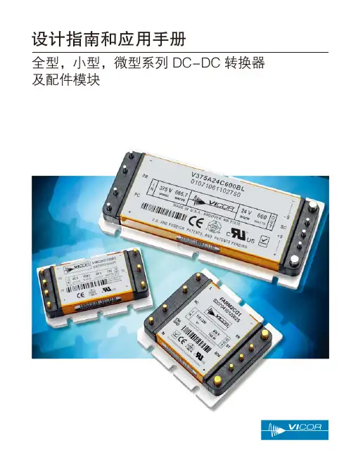
BS62LV256SC-70中文资料
- 格式:pdf
- 大小:336.44 KB
- 文档页数:10
2M X 8 Bit / 1M X 16 Bit CMOS 3.3 Volt-only,Boot Sector Flash MemoryDocument Title2M X 8 Bit / 1M X 16 Bit CMOS 3.3 Volt-only, Boot Sector Flash MemoryRevision HistoryDate Remark Rev. No. History Issue0.0 Initial issue April 1, 2005 Preliminary0.1 Change Vcc_min from 2.7V to 3.0V May 12, 20052M X 8 Bit / 1M X 16 Bit CMOS 3.3 Volt-only,Boot Sector Flash Memory FeaturesSingle power supply operation- Regulated voltage range: 3.0 to 3.6 volt read and write operations for compatibility with high performance 3.3 volt microprocessorsAccess times:- 70/90 (max.)Current:- 9 mA typical active read current- 20 mA typical program/erase current- 200 nA typical CMOS standby- 200 nA Automatic Sleep Mode currentFlexible sector architecture- 16 Kbyte/ 8 KbyteX2/ 32 Kbyte/ 64 KbyteX31 sectors- 8 Kword/ 4 KwordX2/ 16 Kword/ 32 KwordX31 sectors- Any combination of sectors can be erased- Supports full chip erase- Sector protection:A hardware method of protecting sectors to prevent anyinadvertent program or erase operations within that sector. Temporary Sector Unprotect feature allows code changes in previously locked sectorsUnlock Bypass Program Command- Reduces overall programming time when issuingmultiple program command sequenceTop or bottom boot block configurations availableEmbedded Algorithms- Embedded Erase algorithm will automatically erase the entire chip or any combination of designated sectors and verify the erased sectors - Embedded Program algorithm automatically writes and verifies data at specified addressesTypical 100,000 program/erase cycles per sector20-year data retention at 125°C- Reliable operation for the life of the systemCFI (Common Flash Interface) compliant- Provides device-specific information to the system, allowing host software to easily reconfigure for different Flash devicesCompatible with JEDEC-standards- Pinout and software compatible with single-power-supply Flash memory standard- Superior inadvertent write protectionData Polling and toggle bits- Provides a software method of detecting completion of program or erase operationsReady / BUSY pin (RY / BY)- Provides a hardware method of detecting completion of program or erase operations (not available on 44-pin SOP)Erase Suspend/Erase Resume- Suspends a sector erase operation to read data from, or program data to, a non-erasing sector, then resumes the erase operationHardware reset pin (RESET)- Hardware method to reset the device to reading array dataPackage options- 44-pin SOP or 48-pin TSOP (I) or 48-ball TFBGAGeneral DescriptionThe A29L160A is a 16Mbit, 3.3 volt-only Flash memory organized as 2,097,152 bytes of 8 bits or 1,048,576 words of 16 bits each. The 8 bits of data appear on I/O0 - I/O7; the 16 bits of data appear on I/O0~I/O15. The A29L160A is offered in 48-ball FBGA,44-pin SOP and 48-Pin TSOP packages. This device is designed to be programmed in-system with the standard system 3.3 volt VCC supply. Additional 12.0 volt VPP is not required for in-system write or erase operations. However, the A29L160A can also be programmed in standard EPROM programmers.The A29L160A has the first toggle bit, I/O6, which indicates whether an Embedded Program or Erase is in progress, or it is in the Erase Suspend. Besides the I/O6 toggle bit, the A29L160A has a second toggle bit, I/O2, to indicate whether the addressed sector is being selected for erase. The A29L160A also offers the ability to program in the Erase Suspend mode. The standard A29L160A offers access times of 70 and 90ns, allowing high-speed microprocessors to operate without wait states. To eliminate bus contention the device has separate chip enable (CE), write enable (WE) and output enable (OE) controls.The device requires only a single 3.3 volt power supply for both read and write functions. Internally generated and regulated voltages are provided for the program and erase operations.The A29L160A is entirely software command set compatible with the JEDEC single-power-supply Flash standard. Commands are written to the command register using standard microprocessor write timings. Register contents serve as input to an internal state-machine that controls the erase and programming circuitry. Write cycles also internally latch addresses and data needed for the programming and erase operations. Reading data out of the device is similar to reading from other Flash or EPROM devices.Device programming occurs by writing the proper program command sequence. This initiates the Embedded Program algorithm - an internal algorithm that automatically times the program pulse widths and verifies proper program margin.A29L160A SeriesDevice erasure occurs by executing the proper erase command sequence. This initiates the Embedded Erase algorithm - an internal algorithm that automatically preprograms the array (if it is not already programmed) before executing the erase operation. During erase, the device automatically times the erase pulse widths and verifies proper erase margin. The Unlock Bypass mode facilitates faster programming times by requiring only two write cycles to program data instead of four.The host system can detect whether a program or erase operation is complete by observing the RY / BY pin, or by reading the I/O 7 (Data Polling) and I/O 6 (toggle) status bits. After a program or erase cycle has been completed, the device is ready to read array data or accept another command.The sector erase architecture allows memory sectors to be erased and reprogrammed without affecting the data contents of other sectors. The A29L160A is fully erased when shipped from the factory.The hardware sector protection feature disables operations for both program and erase in any combination of the sectors of memory. This can be achieved via programming equipment.The Erase Suspend/Erase Resume feature enables the user to put erase on hold for any period of time to read data from, or program data to, any other sector that is not selected for erasure. True background erase can thus be achieved. The hardware RESET pin terminates any operation in progress and resets the internal state machine to reading array data. The RESET pin may be tied to the system reset circuitry. A system reset would thus also reset the device, enabling the system microprocessor to read the boot-up firmware from the Flash memory.The device offers two power-saving features. When addresses have been stable for a specified amount of time, the device enters the automatic sleep mode. The system can also place the device into the standby mode. Power consumption is greatly reduced in both these modes.Pin ConfigurationsSOPTSOP (I)A18A17A7A6A5A4A3A2A1A0CE VSS OE I/O 0I/O 14I/O 8I/O 7I/O 15(A-1)VSS BYTE A16A15A14A12A11A10A19A8A9A13A 29L 160A M1234567891011121314151629303132333435363738394041424344RESET WE 171819202122282726252423I/O 1I/O 9I/O 2I/O 10I/O 3I/O 11I/O 6I/O 13I/O 5I/O 12I/O 4VCCPin Configurations (continued)TFBGABlock DiagramPin DescriptionsAbsolute Maximum Ratings*Storage Temperature Plastic Packages. . . -65°C to + 150°C Ambient Temperature with Power Applied. -55°C to + 125°C Voltage with Respect to GroundVCC (Note 1) . . . . . . . . . . . . . . . . . . . . ……. . -0.5V to +4.0V A9, OE & (Note 2) . . . . . . . . . . . …. -0.5 to +12.5V All other pins (Note 1) . . . . . . . . . . …. . -0.5V to VCC + 0.5V Output Short Circuit Current (Note 3) . . . . . . . …. . 200mANotes:1. Minimum DC voltage on input or I/O pins is -0.5V. Duringvoltage transitions, input or I/O pins may undershoot VSS to -2.0V for periods of up to 20ns. Maximum DC voltage on input and I/O pins is VCC +0.5V. During voltage transitions, input or I/O pins may overshoot to VCC +2.0V for periods up to 20ns.2. Minimum DC input voltage on A9,OE and RESET is -0.5V. During voltage transitions, A9,OE and RESET may overshoot VSS to -2.0V for periods of up to 20ns.Maximum DC input voltage on A9 is +12.5V which may overshoot to 14.0V for periods up to 20ns.3. No more than one output is shorted at a time. Duration ofthe short circuit should not be greater than one second.*CommentsStresses above those listed under "Absolute Maximum Ratings" may cause permanent damage to this device. These are stress ratings only. Functional operation of this device at these or any other conditions above those indicated in the operational sections of these specification is not implied or intended. Exposure to the absolute maximum rating conditions for extended periods may affect device reliability.Operating RangesCommercial (C) DevicesAmbient Temperature (T A ) . . . . . . . . . . . ….. . . 0°C to +70°CExtended Range DevicesAmbient Temperature (T A )For –I series. . . . . . . . . . . . . . . . . . . . . . . . . . -25°C to +85°C For –U series . . . . . . . . . . . . . . . . . . . . . . . . . -40°C to +85°CVCC Supply VoltagesVCC for all devices . . . . . . . . . . . . . . . . . …...+3.0V to +3.6V Operating ranges define those limits between which the functionally of the device is guaranteed.Device Bus OperationsThis section describes the requirements and use of the device bus operations, which are initiated through the internal command register. The command register itself does not occupy any addressable memory location. The register is composed of latches that store the commands, along with the address and data information needed toexecute the command. The contents of the register serve as inputs to the internal state machine. The state machine outputs dictate the function of the device. The appropriate device bus operations table lists the inputs and control levels required, and the resulting output. The following subsections describe each of these operations in further detail.Table 1. A29L160A Device Bus OperationsL = Logic Low = V IL , H = Logic High = V IH , V ID = 12.0 ± 0.5V, X = Don't Care, D IN = Data In, D OUT = Data Out, A IN = Address In Notes:1. Addresses are A19:A0 in word mode (BYTE =V IH ), A19: A -1 in byte mode (BYTE =V IL ).2. See the “Sector Protection/Unprotection” section and Temporary Sector Unprotect for more information.Word/Byte ConfigurationThe BYTE pin determines whether the I/O pins I/O15-I/O0 operate in the byte or word configuration. If the BYTE pin is set at logic ”1”, the device is in word configuration, I/O15-I/O0 are active and controlled by CE and OE.If the BYTE pin is set at logic “0”, the device is in byte configuration, and only I/O0-I/O7 are active and controlled by CE and OE. I/O8-I/O14 are tri-stated, and I/O15 pin is used as an input for the LSB(A-1) address function. Requirements for Reading Array DataTo read array data from the outputs, the system must drive the CE and OE pins to V IL. CE is the power control and selects the device. OE is the output control and gates array data to the output pins. WE should remain at V IH all the time during read operation. The BYTE pin determines whether the device outputs array data in words and bytes. The internal state machine is set for reading array data upon device power-up, or after a hardware reset. This ensures that no spurious alteration of the memory content occurs during the power transition. No command is necessary in this mode to obtain array data. Standard microprocessor read cycles that assert valid addresses on the device address inputs produce valid data on the device data outputs. The device remains enabled for read access until the command register contents are altered.See "Reading Array Data" for more information. Refer to the AC Read Operations table for timing specifications and to the Read Operations Timings diagram for the timing waveforms, l CC1 in the DC Characteristics table represents the active current specification for reading array data.Writing Commands/Command SequencesTo write a command or command sequence (which includes programming data to the device and erasing sectors of memory), the system must drive WE and CE to V IL, and OE to V IH. For program operations, the BYTE pin determines whether the device accepts program data in bytes or words, Refer to “Word/Byte Configuration” for more information. The device features an Unlock Bypass mode to facilitate faster programming. Once the device enters the Unlock Bypass mode, only two write cycles are required to program a word or byte, instead of four. The “Word / Byte Program Command Sequence” section has details on programming data to the device using both standard and Unlock Bypass command sequence. An erase operation can erase one sector, multiple sectors, or the entire device. The Sector Address Tables indicate the address range that each sector occupies. A "sector address" consists of the address inputs required to uniquely select a sector. See the "Command Definitions" section for details on erasing a sector or the entire chip, or suspending/resuming the erase operation.After the system writes the autoselect command sequence, the device enters the autoselect mode. The system can then read autoselect codes from the internal register (which is separate from the memory array) on I/O7 - I/O0. Standard read cycle timings apply in this mode. Refer to the "Autoselect Mode" and "Autoselect Command Sequence" sections for more information.I CC2 in the DC Characteristics table represents the active current specification for the write mode. The "AC Characteristics" section contains timing specification tables and timing diagrams for write operations.Program and Erase Operation StatusDuring an erase or program operation, the system may check the status of the operation by reading the status bits on I/O7 - I/O0. Standard read cycle timings and I CC read specifications apply. Refer to "Write Operation Status" for more information, and to each AC Characteristics section for timing diagrams.Standby ModeWhen the system is not reading or writing to the device, it can place the device in the standby mode. In this mode, current consumption is greatly reduced, and the outputs are placed in the high impedance state, independent of the OE input.The device enters the CMOS standby mode when the CE & RESET pins are both held at VCC ± 0.3V. (Note that this is a more restricted voltage range than V IH.) If CE and RESET are held at V IH, but not within VCC ± 0.3V, the device will be in the standby mode, but the standby current will be greater. The device requires the standard access time (t CE) before it is ready to read data.If the device is deselected during erasure or programming, the device draws active current until the operation is completed.I CC3 and I CC4 in the DC Characteristics tables represent the standby current specification.Automatic Sleep ModeThe automatic sleep mode minimizes Flash device energy consumption. The device automatically enables this mode when addresses remain stable for t ACC +30ns. The automatic sleep mode is independent of the CE,WE and OE control signals. Standard address access timings provide new data when addresses are changed. While in sleep mode, output data is latched and always available to the system. I CC4 in the DC Characteristics table represents the automatic sleep mode current specification.Output Disable ModeWhen the OE input is at V IH, output from the device is disabled. The output pins are placed in the high impedance state.RESET: Hardware Reset PinThe RESET pin provides a hardware method of resetting the device to reading array data. When the system drives the RESET pin low for at least a period of t RP, the device immediately terminates any operation in progress, tristates all data output pins, and ignores all read/write attempts for the duration of the RESET pulse. The device also resets the internal state machine to reading array data. The operation that was interrupted should be reinitiated once the device is ready to accept another command sequence, to ensure data integrity.Current is reduced for the duration of the RESET pulse. When RESET is held at VSS ± 0.3V, the device draws CMOS standby current (I CC4 ). If RESET is held at V IL but not within VSS ± 0.3V, the standby current will be greater.The RESET pin may be tied to the system reset circuitry. A system reset would thus also reset the Flash memory, enabling the system to read the boot-up firmware from the Flash memory.If RESET is asserted during a program or erase operation, the RY/BY pin remains a “0” (busy) until the internal reset operation is complete, which requires a time t READY (during Embedded Algorithms). The system can thus monitor RY/BYto determine whether the reset operation is RESET is asserted when a program or eraseoperation is not executing (RY/BYpin is “1”), the reset operation is completed within a time of t READY (not during Embedded Algorithms). The system can read data t RH after the RESET pin return to V IH .Refer to the AC Characteristics tables for RESET parameters and diagram.Table 2. A29L160A Top Boot Block Sector Address TableAddress Range (in hexadecimal) Sector A19 A18 A17 A16 A15 A14A13A12Sector Size (Kbytes/ Kwords) Byte Mode (x8)Word Mode (x16)SA0 0 0 0 0 0 X X X 64/32 000000 - 00FFFF 00000 - 07FFF SA1 0 0 0 0 1 X X X 64/32 010000 - 01FFFF 08000 - 0FFFF SA2 0 0 0 1 0 X X X 64/32 020000 - 02FFFF 10000 - 17FFF SA3 0 0 0 1 1 X X X 64/32 030000 - 03FFFF 18000 - 1FFFF SA4 0 0 1 0 0 X X X 64/32 040000 - 04FFFF 20000 - 27FFF SA5 0 0 1 0 1 X X X 64/32 050000 - 05FFFF 28000 - 2FFFF SA6 0 0 1 1 0 X X X 64/32 060000 - 06FFFF 30000 - 37FFF SA7 0 0 1 1 1 X X X 64/32 070000 - 07FFFF 38000 - 3FFFF SA8 0 1 0 0 0 X X X 64/32 080000 - 08FFFF 40000 - 47FFF SA9 0 1 0 0 1 X X X 64/32 090000 - 09FFFF 48000 - 4FFFF SA10 0 1 0 1 0 X X X 64/32 0A0000 - 0AFFFF 50000 - 57FFF SA11 0 1 0 1 1 X X X 64/32 0B0000 - 0BFFFF 58000 - 5FFFF SA12 0 1 1 0 0 X X X 64/32 0C0000 - 0CFFFF 60000 - 67FFF SA13 0 1 1 0 1 X X X 64/32 0D0000 - 0DFFFF 68000 - 6FFFF SA14 0 1 1 1 0 X X X 64/32 0E0000 - 0EFFFF 70000 - 77FFF SA15 0 1 1 1 1 X X X 64/32 0F0000 - 0FFFFF 78000 - 7FFFF SA16 1 0 0 0 0 X X X 64/32 100000 - 10FFFF 80000 - 87FFF SA17 1 0 0 0 1 X X X 64/32 110000 - 11FFFF 88000 - 8FFFF SA18 1 0 0 1 0 X X X 64/32 120000 - 12FFFF 90000 - 97FFF SA19 1 0 0 1 1 X X X 64/32 130000 - 13FFFF 98000 - 9FFFF SA20 1 0 1 0 0 X X X 64/32 140000 - 14FFFF A0000 - A7FFF SA21 1 0 1 0 1 X X X 64/32 150000 - 15FFFF A8000 - AFFFF SA22 1 0 1 1 0 X X X 64/32 160000 - 16FFFF B0000 - B7FFF SA23 1 0 1 1 1 X X X 64/32 170000 - 17FFFF B8000 - BFFFF SA24 1 1 0 0 0 X X X 64/32 180000 - 18FFFF C0000 - C7FFF SA25 1 1 0 0 1 X X X 64/32 190000 - 19FFFF C8000 - CFFFF SA26 1 1 0 1 0 X X X 64/32 1A0000 - 1AFFFF D0000 - D7FFF SA27 1 1 0 1 1 X X X 64/32 1B0000 - 1BFFFF D8000 - DFFFF SA28 1 1 1 0 0 X X X 64/32 1C0000 - 1CFFFF E0000 - E7FFF SA29 1 1 1 0 1 X X X 64/32 1D0000 - 1DFFFF E8000 - EFFFF SA30 1 1 1 1 0 X X X 64/32 1E0000 - 1EFFFF F0000 - F7FFF SA31 1 1 1 1 1 0 X X 32/16 1F0000 - 1F7FFF F8000 - FBFFF SA32 1 1 1 1 1 1 0 0 8/4 1F8000 - 1F9FFF FC000 - FCFFF SA3311111118/41FA000 - 1FBFFFFD000 - FDFFF SA34 1 1 1 1 1 1 1 X 16/8 1FC000 - 1FFFFF FE000 - FFFFFNote:Address range is A19 : A -1 in byte mode and A19 : A0 in word mode. See “Word/Byte Configuration” section.Table 3. A29L160A Bottom Boot Block Sector Address TableSector A19 A18 A17 A16 A15 A14A13A12Sector SizeAddress Range (in hexadecimal)(Kbytes/Kwords) Byte Mode (x8) Word Mode (x16) SA0 0 0 0 0 0 0 0 X 16/8 000000 - 003FFF 00000 - 01FFF SA1 0 0 0 0 0 0 1 0 8/4 004000 - 005FFF 02000 - 02FFF SA2 0 0 0 0 0 0 1 1 8/4 006000 - 007FFF 03000 - 03FFF SA3 0 0 0 0 0 1 X X 32/16 008000 - 00FFFF 04000 - 07FFF SA4 0 0 0 0 1 X X X 64/32 010000 - 01FFFF 08000 - 0FFFF SA5 0 0 0 1 0 X X X 64/32 020000 - 02FFFF 10000 - 17FFF SA6 0 0 0 1 1 X X X 64/32 030000 - 03FFFF 18000 - 1FFFF SA7 0 0 1 0 0 X X X 64/32 040000 - 04FFFF 20000 - 27FFF SA8 0 0 1 0 1 X X X 64/32 050000 - 05FFFF 28000 - 2FFFF SA9 0 0 1 1 0 X X X 64/32 060000 - 06FFFF 30000 - 37FFF SA10 0 0 1 1 1 X X X 64/32 070000 - 07FFFF 38000 - 3FFFF SA11 0 1 0 0 0 X X X 64/32 080000 - 08FFFF 40000 - 47FFF SA12 0 1 0 0 1 X X X 64/32 090000 - 09FFFF 48000 - 4FFFF SA13 0 1 0 1 0 X X X 64/32 0A0000 - 0AFFFF 50000 - 57FFF SA14 0 1 0 1 1 X X X 64/32 0B0000 - 0BFFFF 58000 - 5FFFF SA15 0 1 1 0 0 X X X 64/32 0C0000 - 0CFFFF 60000 - 67FFF SA16 0 1 1 0 1 X X X 64/32 0D0000 - 0DFFFF 68000 - 6FFFF SA17 0 1 1 1 0 X X X 64/32 0E0000 - 0EFFFF 70000 - 77FFF SA18 0 1 1 1 1 X X X 64/32 0F0000 - 0FFFFF 78000 - 7FFFF SA19 1 0 0 0 0 X X X 64/32 100000 - 10FFFF 80000 - 87FFF SA20 1 0 0 0 1 X X X 64/32 110000 - 11FFFF 88000 - 8FFFF SA21 1 0 0 1 0 X X X 64/32 120000 - 12FFFF 90000 - 97FFF SA22 1 0 0 1 1 X X X 64/32 130000 - 13FFFF 98000 - 9FFFF SA23 1 0 1 0 0 X X X 64/32 140000 - 14FFFF A0000 - A7FFF SA24 1 0 1 0 1 X X X 64/32 150000 - 15FFFF A8000 - AFFFF SA25 1 0 1 1 0 X X X 64/32 160000 - 16FFFF B0000 – B7FFF SA26 1 0 1 1 1 X X X 64/32 170000 - 17FFFF B8000 - BFFFF SA27 1 1 0 0 0 X X X 64/32 180000 - 18FFFF C0000 - C7FFF SA28 1 1 0 0 1 X X X 64/32 190000 - 19FFFF C8000 - CFFFF SA29 1 1 0 1 0 X X X 64/32 1A0000 - 1AFFFF D0000 - D7FFF SA30 1 1 0 1 1 X X X 64/32 1B0000 - 1BFFFF D8000 - DFFFF SA31 1 1 1 0 0 X X X 64/32 1C0000 - 1CFFFF E0000 - E7FFF SA32 1 1 1 0 1 X X X 64/32 1D0000 - 1DFFFF E8000 - EFFFF SA33 1 1 1 1 0 X X X 64/32 1E0000 - 1EFFFF F0000 - F7FFF SA34 1 1 1 1 1 X X X 64/32 1F0000 - 1FFFFF F8000 - FFFFF Note:Address range is A19 : A-1 in byte mode and A19 : A0 in word mode. See “Word/Byte Configuration” section.Autoselect ModeThe autoselect mode provides manufacturer and device identification, and sector protection verification, through identifier codes output on I/O7 - I/O0. This mode is primarily intended for programming equipment to automatically match a device to be programmed with its corresponding programming algorithm. However, the autoselect codes can also be accessed in-system through the command register. When using programming equipment, the autoselect mode requires V ID (11.5V to 12.5 V) on address pin A9. Address pins A6, A1, and A0 must be as shown in Autoselect Codes (High Voltage Method) table. In addition, when verifying sector protection, the sector address must appear on the appropriate highest order address bits. Refer to the corresponding Sector Address Tables. The Command Definitions table shows the remaining address bits that are don't care. When all necessary bits have been set as required, the programming equipment may then read the corresponding identifier code on I/O7 - I/O0.To access the autoselect codes in-system, the host system can issue the autoselect command via the command register, as shown in the Command Definitions table. This method does not require V ID. See "Command Definitions" for details on using the autoselect mode.Table 4. A29L160A Autoselect Codes (High Voltage Method)L=Logic Low= V IL, H=Logic High=V IH, SA=Sector Address, X=Don’t Care.Note: The autoselect codes may also be accessed in-system via command sequences.Sector Protection/UnprotectionThe hardware sector protection feature disables both program and erase operations in any sector. The hardware sector unprotection feature re-enables both program and erase operations in previously protected sectors.It is possible to determine whether a sector is protected or unprotected. See “Autoselect Mode” for details.Sector protection / unprotection can be implemented via two methods. The primary method requires VID on the RESET pin only, and can be implemented either in-system or via programming equipment. Figure 2 shows the algorithm and the Sector Protect / Unprotect Timing Diagram illustrates the timing waveforms for this feature. This method uses standard microprocessor bus cycle timing. For sector unprotect, all unprotected sectors must first be protected prior to the first sector unprotect write cycle. The alternate method must be implemented using programming equipment. The procedure requires a high voltage (V ID) on address pin A9 and the control pins.The device is shipped with all sectors unprotected.It is possible to determine whether a sector is protected or unprotected. See "Autoselect Mode" for details.Hardware Data ProtectionThe requirement of command unlocking sequence for programming or erasing provides data protection against inadvertent writes (refer to the Command Definitions table). In addition, the following hardware data protection measures prevent accidental erasure or programming, which might otherwise be caused by spurious system level signals during V CC power-up transitions, or from system noise. The device is powered up to read array data to avoid accidentally writing data to the array.Write Pulse "Glitch" ProtectionNoise pulses of less than 5ns (typical) on OE, CE or WEdo not initiate a write cycle.Logical InhibitWrite cycles are inhibited by holding any one of OE=V IL, CE = V IH or WE = V IH. To initiate a write cycle, CE and WE must be a logical zero while OE is a logical one.Power-Up Write InhibitIf WE = CE = V IL and OE = V IH during power up, the device does not accept commands on the rising edge of WE. The internal state machine is automatically reset to reading array data on the initial power-up. Temporary Sector UnprotectThis feature allows temporary unprotection of previous protected sectors to change data in-system. The Sector Unprotect mode is activated by setting the RESET pin to V ID. During this mode, formerly protected sectors can be programmed or erased by selecting the sector addresses. Once V ID is removed from the RESET pin, all the previously protected sectors are protected again. Figure 1 shows the algorithm, and the Temporary Sector Unprotect diagram shows the timing waveforms, for this feature.Notes:1. All protected sectors unprotected.2. All previously protected sectors are protected once again.Figure 1. Temporary Sector Unprotect OperationFigure 2. In-System Sector Protect/Unprotect AlgorithmsCommon Flash Memory Interface (CFI)The Common Flash Interface (CFI) specification outlines device and host system software interrogation handshake, which allows specific vendor-specified software algorithms to be used for entire families of devices. Software support can then be device-independent, JEDEC ID-independent, and forward- and backward-compatible for the specified flash device families. Flash vendors can standardize their existing interface for long-term compatibility.This device enters the CFI Query mode when the system writes the CFI Query command, 98h, to address 55h in word mode (or address AAh in byte mode), any time the device is ready to read array data. The system can read CFI information at the addresses given in Table 5-8. In word mode, the upper address bits (A7-MSB) must be all zeros. To terminate reading CFI data, the system must write the reset command.The system can also write the CFI query command when the device is in the autoselect mode. The device enters the CFI query mode, and the system can read CFI data at the addresses given in Table 5-8. The system must write the reset command to return the device to the autoselect mode.Table 5. CFI Query Identification StringAddresses (Word Mode)Addresses(Byte Mode)Data Description10h 11h 12h 20h22h24h0051h0052h0059hQuery Unique ASCII string “QRY”13h 14h 26h28h0002h0000hPrimary OEM Command Set15h 16h 2Ah2Ch0040h0000hAddress for Primary Extended Table17h 18h 2Eh30h0000h0000hAlternate OEM Command Set (00h = none exists)19h 1Ah 32h34h0000h0000hAddress for Alternate OEM Extended Table (00h = none exists) Table 6 System Interface StringAddresses (Word Mode)Addresses(Byte Mode)Data Description1Bh 36h 0027h VCC Min. (write/erase)I/O7- I/O4 : volt, I/O3- I/O0: 100 millivolt1Ch 38h 0036h VCC Max. (write/erase)I/O7- I/O4: volt, I/O3- I/O0: 100 millivolt1Dh 3Ah 0000h Vpp Min. voltage (00h = no Vpp pin present)1Eh 3Ch 0000h Vpp Max. voltage (00h = no Vpp pin present)1Fh 3Eh0004hTypical timeout per single byte/word write 2Nµs20h 40h0000hTypical timeout for Min. size buffer write 2Nµs (00h = not supported) 21h 42h 000Ah Typical timeout per individual block erase 2N ms22h 44h 0000h Typical timeout for full chip erase 2N ms (00h = not supported)23h 46h 0005h Max. timeout for byte/word write 2N times typical24h 48h 0000h Max. timeout for buffer write 2N times typical25h 4Ah 0004h Max. timeout per individual block erase 2N times typical26h 4Ch 0000h Max. timeout for full chip erase 2N times typical (00h = not supported)。

ICSI reserves the right to make changes to its products at any time without notice in order to improve design and supply the best possible product. We assume no responsibility for any errors which may appear in this publication. © Copyright 2000, Integrated Circuit Solution Inc.DESCRIPTIONThe 1+51 IS62LV2568L and IS62LV2568LL are low powerand low V CC , 262,144-bit words by 8 bits CMOS static RAMs.They are fabricated using 1+51's high-performance CMOS technology. This highly reliable process coupled with innova-tive circuit design techniques, yields higher performance and low power consumption devices.When CE1 is HIGH or CE2 is LOW (deselected), the device assumes a standby mode at which the power dissipation can be reduced by using CMOS input levels.Easy memory expansion is provided by using two Chip Enable inputs, CE1 and CE2. The active LOW Write Enable (WE )controls both writing and reading of the memory.The IS62LV2568L and IS62LV2568LL are available in 32-pin 8*20mm TSOP-1, 8*13.4mm TSOP-1 and 48-pin 6*8mm TF-BGA.FEATURESAccess times of 55, 70, 100 nsLow active power: 126 mW (max, L, LL)Low standby power: 36 µW (max, L) and 7.2µW (max, LL) CMOS standbyLow data retention voltage: 1.5V (min.) Available in Low Power (-L) and Ultra-Low Power (-LL)Output Enable (OE ) and two Chip Enable TTL compatible inputs and outputs Single 2.7V-3.6V power supplyAvailable in the 32-pin 8x20mm TSOP-1, 32-pin 8x13.4mm TSOP-1 and 48-pin 6*8mm TF-BGA2Integrated Circuit Solution Inc.IS62LV2568L IS62LV2568LLPIN CONFIGURATIONS32-Pin 8*20mm TSOP-1, 8*13.4mm STSOP-1PIN DESCRIPTIONSA0-A17Address Inputs CE1Chip Enable 1 Input CE2Chip Enable 2 Input OE Output Enable Input WE Write Enable Input I/O0-I/O7Data Input/Output NC No Connection Vcc Power GNDGround48-Pin 6*8mm TF-BGAOPERATING RANGERangeAmbient TemperatureV CCCommercial 0°C to +70°C 2.7V - 3.6V Industrial40°C to +85°C2.7V -3.6VIS62LV2568L IS62LV2568LLABSOLUTE MAXIMUM RATINGS (1)Symbol ParameterValueUnit V TERM Terminal Voltage with Respect to GND 0.5 to Vcc + 0.5V V CC Vcc related to GND0.3 to +4.0V T BIAS Temperature Under Bias 40 to +85°C T STG Storage Temperature 65 to +150°C P TPower Dissipation0.7WNotes:1.Stress greater than those listed under ABSOLUTE MAXIMUM RATINGS may cause permanent damage to the device. This is a stress rating only and functional operation of the device at these or any other conditions above those indicated in the operational sections of this specification is not implied. Exposure to absolute maximum rating conditions for extended periods may affect reliability.CAPACITANCE (1)Symbol Parameter Conditions Max.Unit C IN Input Capacitance V IN = 0V 6pF C OUTOutput CapacitanceV OUT = 0V8pFNotes:1.Tested initially and after any design or process changes that may affect these parameters.DC ELECTRICAL CHARACTERISTICS (Over Operating Range)Symbol ParameterTest ConditionsMin.Max.Unit V OH Output HIGH Voltage V CC = Min., I OH = 1.0 mA 2.2 V V OL Output LOW Voltage V CC = Min., I OL = 2.1 mA0.4V V IH Input HIGH Voltage 2.2V CC + 0.3V V IL (1)Input LOW Voltage (1) 0.30.4V I LI Input Leakage GND ≤ V IN ≤ V CC 11µA I LOOutput LeakageGND ≤ V OUT ≤ V CC11µANotes:1.V IL =2.0V for pulse width less than 10 ns.TRUTH TABLEModeWE CE1CE2OE I/O OperationVcc Current Not Selected X H X X High-Z I SB , I SB (Power-down)X X L X High-Z I SB , I SBOutput Disabled H L H H High-Z I CC Read H L H L D OUT I CC WriteLLHXD INI CCIS62LV2568LIS62LV2568LLIS62LV2568L POWER SUPPLY CHARACTERISTICS(1)(Over Operating Range)-55-70-100Symbol Parameter Test Conditions Min.Max.Min.Max.Min.Max.UnitI CC Vcc Dynamic Operating V CC = Max.,Com. 40 30 20mASupply Current I OUT = 0 mA, f = f MAX Ind. 45 35 25I SB TTL Standby Current V CC = Max.,Com. 0.4 0.4 0.4mA(TTL Inputs)V IN = V IH or V IL,Ind. 1.0 1.0 1.0CE1≥ V IH or CE2 ≤ V IL, f = 0I SB CMOS Standby V CC = Max., f = 0Com. 35 35 35µACurrent (CMOS Inputs)CE1≥ V CC 0.2V,Ind. 50 50 50CE2 ≤ 0.2V,or V IN≥ V CC 0.2V, V IN≤ 0.2VNote:1.At f = f MAX, address and data inputs are cycling at the maximum frequency, f = 0 means no input lines change.IS62LV2568LL POWER SUPPLY CHARACTERISTICS(1)(Over Operating Range)-55-70-100Symbol Parameter Test Conditions Min.Max.Min.Max.Min.Max.UnitI CC Vcc Dynamic Operating V CC = Max.,Com. 40 30 20mASupply Current I OUT = 0 mA, f = f MAX Ind. 45 35 25I SB TTL Standby Current V CC = Max.,Com. 0.4 0.4 0.4mA(TTL Inputs)V IN = V IH or V IL,Ind. 1.0 1.0 1.0CE1≥ V IH or CE2 ≤ V IL, f = 0I SB CMOS Standby V CC = Max., f = 0Com. 10 10 10µACurrent (CMOS Inputs)CE≥ V CC 0.2V,Ind. 15 15 15CE2 ≤ 0.2V,or V IN≥ V CC 0.2V, V IN≤ 0.2VNote:1.At f = f MAX, address and data inputs are cycling at the maximum frequency, f = 0 means no input lines change.4Integrated Circuit Solution Inc.IS62LV2568LIS62LV2568LLREAD CYCLE SWITCHING CHARACTERISTICS(1)(Over Operating Range)-55-70-100Symbol Parameter Min.Max.Min.Max.Min.Max.Unit t RC Read Cycle Time55 70 100 nst AA Address Access Time 55 70 100nst OHA Output Hold Time10 10 15 nst ACE1CE1 Access Time 55 70 100nst ACE2CE2 Access Time 55 70 100nst DOE OE Access Time 30 35 50nst LZOE(2)OE to Low-Z Output5 5 5 nst HZOE(2)OE to High-Z Output 20025030nst LZCE1(2)CE1 to Low-Z Output10 10 10 nst LZCE2(2)CE2 to Low-Z Output10 10 10 nst HZCE(2)CE1 or CE2 to Low-Z Output020025030nsNotes:1.Test conditions assume signal transition times of 5 ns or less, timing reference levels of 1.5V, input pulse levelsof 0.4V to 2.2V and output loading specified in Figure 1.2.Tested with the load in Figure 2. Transition is measured ±500 mV from steady-state voltage. Not 100% tested.AC TEST CONDITIONSParameter UnitInput Pulse Level0.4V to 2.2VInput Rise and Fall Times 5 nsInput and Output Timing 1.5Vand Reference LevelOutput Load See Figures 1 and 2AC TEST LOADSFigure 1Figure 26Integrated Circuit Solution Inc.IS62LV2568L IS62LV2568LLNotes:1.WE is HIGH for a Read Cycle.2.The device is continuously selected. OE , CE1 = VIL , CE2 = V IL .3.Address is valid prior to or coincident with CE1 LOW and CE2 HIGH transitions.AC WAVEFORMS(1,3)AC TEST LOADSREAD CYCLE NO.1(1,2)IS62LV2568L IS62LV2568LL-55-70-100SymbolParameter Min.Max.Min.Max.Min.Max Unit t WC Write Cycle Time 55 70 100 ns t SCE 1CE1 to Write End 45 65 80 ns t SCE 2CE2 to Write End45 65 80 ns t AW Address Setup Time to Write End 45 65 80 ns t HA Address Hold from Write End 0 0 0 ns t SA Address Setup Time 0 0 0 ns t PWE (4)WE Pulse Width 50 55 70 ns t SD Data Setup to Write End 25 30 40 ns t HDData Hold from Write End0 0 0 ns t HZWE (3)WE LOW to High-Z Output 25 25 30ns t LZWE (3)WE HIGH to Low-Z Output555nsNotes:1.Test conditions assume signal transition times of 5 ns or less, timing reference levels of 1.5V, input pulse levels of 0.4V to2.2V and output loading specified in Figure 1.2.Tested with the load in Figure 2. Transition is measured ±500 mV from steady-state voltage. Not 100% tested.3.The internal write time is defined by the overlap of CE1 LOW, CE2 HIGH and WE LOW. All signals must be in valid states to initiate a Write, but any one can go inactive to terminate the Write. The Data Input Setup and Hold timing are referenced to the rising or falling edge of the signal that terminates the Write.4.Tested with OE HIGH.WRITE CYCLE SWITCHING CHARACTERISTICS (1,2) (Over Operating Range, Standard and Low Power)AC WAVEFORMSWRITE CYCLE NO. 1 (WE Controlled )(1,2)IS62LV2568LIS62LV2568LLWRITE CYCLE NO. 2 (CE1, CE2 Controlled)(1,2)Notes:1.The internal write time is defined by the overlap of CE1 LOW, CE2 HIGH and WE LOW. All signals must be in valid statesto initiate a Write, but any one can go inactive to terminate the Write. The Data Input Setup and Hold timing are referenced to the rising or falling edge of the signal that terminates the Write.2.I/O will assume the HIGH-z state if OE =V IH.8Integrated Circuit Solution Inc.IS62LV2568L IS62LV2568LLDATA RETENTION SWITCHING CHARACTERISTICSSymbolParameterTest ConditionMin.Max.Unit V DRVcc for Data Retention See Data Retention Waveform 1.5 3.6V I DRData Retention CurrentVcc = 2.0V, CE1 ≥ Vcc 0.2VCom. (-L) 20µA Com. (-LL) 5µA Ind. (-L) 25µA Ind. (-LL)7µA t SDR Data Retention Setup Time See Data Retention Waveform 0ns t RDRRecovery TimeSee Data Retention Waveformt RCnsDATA RETENTION WAVEFORM (CE2 Controlled)DATA RETENTION WAVEFORM (CE1Controlled)IS62LV2568L IS62LV2568LLORDERING INFORMATION Commercial Range: 0°C to +70°C Speed (ns)Order Part No.Package55IS62LV2568L-55T8*20mm TSOP-1IS62LV2568L-55H8*13.4mm TSOP-1IS62LV2568L-55B6*8mm TF-BGA 70IS62LV2568L-70T8*20mm TSOP-1IS62LV2568L-70H8*13.4mm TSOP-1IS62LV2568L-70B6*8mm TF-BGA 100IS62LV2568L-100T8*20mm TSOP-1IS62LV2568L-100H8*13.4mm TSOP-1IS62LV2568L-100B6*8mm TF-BGA Industrial Range: -40°C to +85°CSpeed (ns)Order Part No.Package55IS62LV2568L-55TI8*20mm TSOP-1IS62LV2568L-55HI8*13.4mm TSOP-1IS62LV2568L-55BI6*8mm TF-BGA70IS62LV2568L-70TI8*20mm TSOP-1IS62LV2568L-70HI8*13.4mm TSOP-1IS62LV2568L-70BI6*8mm TF-BGA100IS62LV2568L-100TI8*20mm TSOP-1IS62LV2568L-100HI8*13.4mm TSOP-1IS62LV2568L-100BI6*8mm TF-BGAIntegrated Circuit Solution Inc.HEADQUARTER:NO.2, TECHNOLOGY RD. V, SCIENCE-BASED INDUSTRIAL PARK,HSIN-CHU, TAIWAN, R.O.C.TEL: 886-3-5780333Fax: 886-3-5783000BRANCH OFFICE:7F, NO. 106, SEC. 1, HSIN-TAI 5TH ROAD,HSICHIH TAIPEI COUNTY, TAIWAN, R.O.C.TEL: 886-2-26962140FAX: 886-2-2696225210Integrated Circuit Solution Inc.。
行号物料代码物料名称单位数量1CL.01.09.0045二极管(IN5819/1A/40V/0.4间距)个172 2CL.01.09.0046发光二极管(0603-绿灯)PLC个3,530 3CL.01.09.0048二极管(SMD BZT52-C11)PLC个2,306 4CL.01.09.0052二极管(MBR1535CT)个315CL.01.10.0043桥(DF06M/1A/600V(DB107/1A/700V))个2,261 6CL.01.12.0005MOS管(SMD IRFR9024N)PLC个2,000 7CL.01.12.0006MOS管(SMD ST3407)PLC个448CL.01.13.0019三极管(SMD CAT810LTBI)PLC个2,881 9CL.01.13.0020三极管(SMD MMBT6427LT1/0.5A/40V)PLC个3,174 10CL.01.13.0022三极管(2SC2383)PLC个732 11CL.01.13.0025三极管(SMD MJD112 TO252)PLC用个1,964 12CL.01.14.0019稳压块(SMD LM2575S-5V)个4513CL.01.15.0019稳压管(SMD REF3020AIDBZ)PLC个3,164 14CL.01.15.0020稳压管(LM385BLP-1.2)个1,128 15CL.01.15.0026稳压管(SMD REF3040AIDBZ)个3416CL.01.15.0027稳压管(LM385BLP-2.5)个989 17CL.01.15.0028稳压管(P6KE170A)个9018CL.01.15.0029稳压管(P6KE200A)个800 19CL.01.16.0082集成电路(SMD SN74AHC32DR)PLC个2,050 20CL.01.16.0083集成电路(SMD SN74AHC14DR)PLC个4,628 21CL.01.16.0084集成电路(SMD DAC7612UB)PLC个214 22CL.01.16.0085集成电路(SMD SN74AHCIG14DBV)PLC个2823CL.01.16.0086集成电路(SMD ADS1110A0IDBVT)PLC个3,084 24CL.01.16.0087集成电路(SMD PCA82C250T)PLC个3,869 25CL.01.16.0088集成电路(SMD BS62LV256SC-70)PLC个2,54226CL.01.16.0089集成电路(SMD FM3164-S)PLC个2627CL.01.16.0090集成电路(SMD LM2675M-5.0)PLC个182 28CL.01.16.0091集成电路(SMD AT93C46-10SI-2.7)PLC个3,009 29CL.01.16.0092集成电路(SMD MCP2515-I/ST)PLC个2,297 30CL.01.16.0093集成电路(SMD SN74HC244DW)PLC个1,180 31CL.01.16.0094集成电路(SMD DG409DY)PLC个2,568 32CL.01.16.0095集成电路(TNY268P)个2,267 33CL.01.16.0096集成电路(ICL7662CPA)个420 34CL.01.16.0099集成电路(SMD ZT232LEEN)PLC个497 35CL.01.16.0101集成电路(无铅 SMD INA143UA)PLC个2,441 36CL.01.16.0105集成电路(无铅 SMD M29F102BB70K1)个7637CL.01.16.0111集成电路(SMD TL16C550DIPT)PLC个1,950 38CL.01.16.0112集成电路(SMD SN74AHC1G00DBV)PLC个2,500 39CL.01.16.0113集成电路(SMD SN74AHC1G08DBV)PLC个2,492 40CL.01.16.0114集成电路(SMD SN74HC273PW)PLC个1,500 41CL.01.16.0116集成电路(TNY264PN)个266 42CL.01.16.0117集成电路(TNY266PN)个270 43CL.01.16.0119集成电路(SMD FM24C256-S)PLC个1,185 44CL.01.16.0120集成电路(SMD ISL1208IB8)PLC个1,612 45CL.01.16.0121集成电路(SMD AM29F200BB-70EI)PLC个2,512 46CL.01.16.0122集成电路(SMD BS616LV1010EI-70)PLC个1,033 47CL.01.16.0123集成电路(SMD SN74AC573PW 窄体)PLC个5,000 48CL.01.16.0125集成电路(SMD INA126UA)个2,429 49CL.01.16.0126集成电路(SMD ADS1112IDGST)PLC个550CL.01.16.0127集成电路(SMD 74HC00)个4651CL.01.16.0128集成电路(SMD 74HCT245)个4552CL.01.16.0129集成电路(SMD CAT24WC64J)个853CL.01.16.0130集成电路(SMD SPC3)个4654CL.01.16.0131集成电路(SMD GAL16V8D)PLC个414 55CL.01.16.0135集成电路(SMD LM71CIMF)个6356CL.01.16.0136集成电路(SMD AM29F040B-70JC)个2457CL.01.16.0138集成电路(散新:SMD HY6264ALJ-10HY6264ALJ个4558CL.01.16.0159集成电路(SMD SN74HC273DW)PLC个150 59CL.01.16.0165集成电路(SMD AM29F040B-70JF)个750 60CL.01.16.0168集成电路(SMD LTC2627IDE-1#PBF)PLC个791CL.01.01.0012自恢复保险(RF30-135B/1.35A/30V)个325 2CL.01.01.0013自恢复保险(RF30-090B(0.9A/30V/RUE090))个488 3CL.01.01.0014自恢复保险(RF30-300B 3A/30V)个334CL.01.01.0015保险慢融(CIS T2A/250V 5*20)个361 5CL.01.03.0002磁珠(SMD CBW453215U121B)个1,781 6CL.01.06.0011晶振(SMD 25.000MHZ/5V-50ppm)个553 7CL.01.06.0012晶振 KDS(32.768KHz/12.5pF/5ppm)个828CL.01.06.0013晶振(AT-38/25.000MHZ/30PF-30PPM)个109 9CL.01.06.0024晶振(25.000M 5V 4PIN)个165 10CL.01.24.0022共模电感(3.3UH/0.6A)个478 11CL.01.24.0023工字型电感(47UH/1.5A)个393 12CL.01.24.0033电感(10UH/3A)个2113CL.01.25.0007编码开关(R7H3-10RB-V-B)个3214CL.03.02.0159变压器(ELEE19-1)个295 15CL.03.02.0161变压器(EPEI22-2)个24016CL.03.02.0193变压器(EPEI22-1S)个274 17CL.03.02.0220变压器(EPEI22-3)个1018CL.03.02.0221变压器(EPEI22-4)个219CL.03.02.0230变压器(EPEI22-1T)个520CL.03.11.0038摇柄开关(UT-4-T2CK-2-H)个320 21CL.04.02.0068简牛插座(配菏泽线用)2*8个482 22CL.04.02.0077插座排母(F/H 2.0 2*18 SMT H=4.3 PA6T)个136 23CL.04.02.0078插座排母(F/H 2.0 2*10 SMT H=4.3 PA6T)个222 24CL.04.02.0079插座排母(F/H 2.54 1*17 H=5.0 PA6T)蜈蚣个562 25CL.04.02.0080插座排母(SMD F/H2.54 2*14 H=5.0SMT)个3626CL.04.02.0081插座排母(SMD F/H2.54 1*14H=5.0蜈蚣脚=5.0个415 27CL.04.03.0023短路针排针(P/H 2.0 2*10*2 L=17.5 PA6T)只354 28CL.04.03.0024短路针排针(P/H 2.0 2*18*2 L=17.5 PA6T)只256 29CL.04.03.0025短路针排针(P/H 2.54 1*17*2 L=30.0 PA6T)只566 30CL.04.03.0026短路针排针(P/H2.54 2*14*2 L=14.0)只4631CL.04.03.0027短路针排针(P/H 2.54 1*14*2 180D L=30.0 P只388 32CL.04.05.0059插接件(DR9 孔)个151CL.01.01.0004保险管(3A)个198 2CL.01.01.0018保险夹(5*20)个724CL.04.05.0050插接件(DP9 PIN-F 母头 PLC用)个301CL.01.17.0014CPU(SMD SAK-164CI-LM CA+)PLC个12CL.01.17.0015CPU(SMD AT89S51-24AI)PLC个252 3CL.01.17.0016CPU(SMD AT89S52-24AI)PLC个1,5464CL.01.17.0017电源芯片(SMD LM317MKTPR)PLC个3,002 5CL.01.17.0018CPU(SMD SAK-XE164FM-72F80L AA)PLC个36CL.01.17.0019CPU(SMD SAF-C164CI-LM CA+)PLC个128 7CL.01.17.0020电源芯片(TNY279P)个418CL.01.17.0021电源芯片(TNY278P)个329CL.01.17.0022电源芯片(B0505S-1W)个2910CL.01.17.0023CPU (SMD STC12C5A32S2)PLC个4311CL.01.17.0029CPU(SMD AT89S51-24AU)个1,600 12CL.01.17.0032CPU(SMD LM317DCYR)个2,463 13CL.01.18.0025光耦(SMD HCPL-0600-500E)个1,500 14CL.02.02.0075电容(334K/275V(0.33uF/275V))个546 15CL.02.02.0076电容(3.3nF/250V)个709 16CL.02.02.0077电解电容(47uF/400V/20% D16*L20)个326 17CL.02.02.0078电解电容(33uF/400V/20% D16*L20)个284 18CL.02.02.0079电容(22nF/500V(630V)/20%/0.4)个246 19CL.02.03.0047法拉电容(0.33F/5.5V)个419 20CL.02.04.0064磁介电容(0805-15P/50V)PLC个2,611 21CL.02.07.0161电阻(RC-ML08W122JT/风华)(排阻)PLC个5022CL.02.07.0163电阻(YC164-JR-071K5L)网络电阻(阻排)PL个5,000 23CL.02.08.0056电阻(MF-25-680KΩ 1/4W)个348 24CL.02.08.0057电阻(MF-25-2MΩ 1/4W)个34925CL.02.08.0058电阻(RN-60-50KΩ 1/4W 0.1%)个433 26CL.02.08.0059电阻(RN-60-10KΩ 1/4W 0.1%)个443 27CL.02.08.0060电阻(RN-60-2KΩ 1/4W 0.1%)个324 28CL.02.08.0061电阻(RN-60-1KΩ 1/4W 0.1%)个307 29CL.02.08.0062电阻(RN-60-100Ω 1/4W 0.1%)个255 30CL.02.08.0063电阻(RN-60-250Ω 1/4W 0.1%)个454 31CL.02.08.0092精密直插电阻(500Ω 1/4W0.1%)个190 32CL.02.08.0097电阻(无铅 1/2W 200K)PLC个112 33CL.02.08.0098电阻(无铅 1/2W 30R)PLC个123 34CL.02.08.0112电阻(无铅1/4W 300Ω)个908 35CL.02.08.0113电阻(无铅1/2W 120Ω)个517 36CL.02.12.0004压敏电阻(FNR-07K390/39V/0.2)个980 37CL.02.12.0005压敏电阻(10D471K/470V)个607 38CL.02.13.0020水泥电阻(无铅RX27-3-7W-120ΩJ)个605 39CL.04.04.0157端子(DG129-5.08-03 绿)位8,130 40CL.04.04.0174端子(DG129-5.08-02P-13-07A(H)黑)位2,438 41CL.04.04.0175端子(DG129-5.08-03P-13-07A(H)黑)位4,630 42CL.04.04.0220端子(DG129-5.08-13P-13-60AH)条943CL.04.04.0221端子(DG129-5.08-08P-13-60AH)条944CL.04.04.0222端子(DG129-5.08-19P-13-60AH)条9调出仓库调入仓库调入仓位订单单号呆滞材料库材料库A呆滞材料库材料库A呆滞材料库材料库A呆滞材料库材料库A呆滞材料库材料库A呆滞材料库材料库A呆滞材料库材料库A呆滞材料库材料库A呆滞材料库材料库A呆滞材料库材料库A呆滞材料库材料库A呆滞材料库材料库A呆滞材料库材料库A呆滞材料库材料库A呆滞材料库材料库A呆滞材料库材料库A呆滞材料库材料库A呆滞材料库材料库A呆滞材料库材料库A呆滞材料库材料库A呆滞材料库材料库A呆滞材料库材料库A呆滞材料库材料库A呆滞材料库材料库A呆滞材料库材料库A呆滞材料库材料库A 呆滞材料库材料库A 呆滞材料库材料库A 呆滞材料库材料库A 呆滞材料库材料库A 呆滞材料库材料库A 呆滞材料库材料库A 呆滞材料库材料库A 呆滞材料库材料库A 呆滞材料库材料库A 呆滞材料库材料库A 呆滞材料库材料库A 呆滞材料库材料库A 呆滞材料库材料库A 呆滞材料库材料库A 呆滞材料库材料库A 呆滞材料库材料库A 呆滞材料库材料库A 呆滞材料库材料库A 呆滞材料库材料库A 呆滞材料库材料库A 呆滞材料库材料库A 呆滞材料库材料库A 呆滞材料库材料库A 呆滞材料库材料库A 呆滞材料库材料库A呆滞材料库材料库A 呆滞材料库材料库A 呆滞材料库材料库A 呆滞材料库材料库A 呆滞材料库材料库A 呆滞材料库材料库A 呆滞材料库材料库A 呆滞材料库材料库A 呆滞材料库材料库A 呆滞材料库材料库A 呆滞材料库材料库A 呆滞材料库材料库A 呆滞材料库材料库A 呆滞材料库材料库A 呆滞材料库材料库A 呆滞材料库材料库A 呆滞材料库材料库A 呆滞材料库材料库A 呆滞材料库材料库A 呆滞材料库材料库A 呆滞材料库材料库A 呆滞材料库材料库A 呆滞材料库材料库A 呆滞材料库材料库A呆滞材料库材料库A 呆滞材料库材料库A 呆滞材料库材料库A 呆滞材料库材料库A 呆滞材料库材料库A 呆滞材料库材料库A 呆滞材料库材料库A 呆滞材料库材料库A 呆滞材料库材料库A 呆滞材料库材料库A 呆滞材料库材料库A 呆滞材料库材料库A 呆滞材料库材料库A 呆滞材料库材料库A 呆滞材料库材料库A 呆滞材料库材料库A 呆滞材料库材料库A 呆滞材料库材料库A 呆滞材料库材料库A 呆滞材料库材料库A 呆滞材料库材料库A 呆滞材料库材料库A 呆滞材料库材料库A呆滞材料库材料库A 呆滞材料库材料库A 呆滞材料库材料库A 呆滞材料库材料库A 呆滞材料库材料库A 呆滞材料库材料库A 呆滞材料库材料库A 呆滞材料库材料库A 呆滞材料库材料库A 呆滞材料库材料库A 呆滞材料库材料库A 呆滞材料库材料库A 呆滞材料库材料库A 呆滞材料库材料库A 呆滞材料库材料库A 呆滞材料库材料库A 呆滞材料库材料库A 呆滞材料库材料库A 呆滞材料库材料库A 呆滞材料库材料库A 呆滞材料库材料库A呆滞材料库材料库A 呆滞材料库材料库A 呆滞材料库材料库A 呆滞材料库材料库A 呆滞材料库材料库A 呆滞材料库材料库A 呆滞材料库材料库A 呆滞材料库材料库A 呆滞材料库材料库A 呆滞材料库材料库A 呆滞材料库材料库A 呆滞材料库材料库A 呆滞材料库材料库A 呆滞材料库材料库A 呆滞材料库材料库A 呆滞材料库材料库A 呆滞材料库材料库A 呆滞材料库材料库A 呆滞材料库材料库A 呆滞材料库材料库A。
!"# $%&' ( ' %)) (* +,(!" #$%& ' ( ) * &+$ , " $%- * . # .$% (/ # ' ( ,01&2 3 .%' $ %%$( 01&2 3 %$&4 %%$(0 -# 3 1 / &(45- %%$( " 6'+7 /#$$4 & $// ' $ , (/ 01&2 3 (/ 01&2 3" & ' # .$% 4 .( .7$( 7'# '/ 4$/$*$ $4" 7%$$ / & $ # / &(4 #& '5*$" 8 **- / & ' #$%& ' (" & & %$ $( ' ( / ##*- ) * &+$ &/ * . &/ " &/- $2#&(/' ( .' 7 9 9 &(4 # ' (/7$ '/ & 7'+7 #$%: % &( $9 )$%- * . # .$% 1 & ' ;&(4 $// 1$ %- %+&('<$4 &/ 9 . %4/ 5- ! 5' /&(4 #$%& $/ :% & .'4$ %&(+$ : / ##*- ) * &+$4)&( $4 1 $ 7( * +- &(4 '% ' $ 7('= $/ #% )'4$ 5 7 7'+7/#$$4 &(4 * . # .$% :$& %$/ .' 7 & -#' &* 1 / &(45- %%$( : &(4 &2' & $// ' $ : (/ '( #$%& ' (&/- $ %- $2#&(/' ( '/ #% )'4$4 5- &( & ')$ > 7'#$(&5*$ 0 39 &( & ')$ 6 ?6 7'# $(&5*$ 0 39 &(4 & ')$ > # $(&5*$ 0 3 &(4 7%$$ / & $ # 4%')$%/7$ 7&/ &( & & ' # .$% 4 .( :$& %$9 %$4 '(+ 7$# .$% (/ # ' ( /'+(':' &( *- .7$( 7'# '/ 4$/$*$ $47$ '/ &)&'*&5*$ '( : % 9 @ / &(4&%4 #'( '* *&/ ' 9 '* *&/ ' 9 ! 2 &(4 ! 2!!!!!!"# $"% &" ' (' )"* & + , ,- . &"* & $"( (( (" "*!!! !%$//$/ +%$& $% 7&( 7 /$ *'/ $4 (4$% A 1 B 1A1; C? &- & /$ #$% &($( 4& &+$ 7$ 4$)' $ 7'/ '/ &/ %$// %& '(+ (*- &(4 : ( ' (&* #$%& ' ( : 7$ 4$)' $ & 7$/$ % &(- 7$% (4' ' (/ &5 )$ 7 /$ '(4' & $4 '( 7$ #$%& ' (&*/$ ' (/ : 7'/ /#$ ':' & ' ( '/ ( ' #*'$4 2# / %$ &5/ * $&2' %& '(+ (4' ' (/ : % $2 $(4$4 #$%' 4/ &- &::$ %$*'&5'*' -7'/ #&%& $ $% '/ + &%&( $$4 &(4 ( $/ $4! " # $ % &'( ! ! " ) &(* & + ,#( ," " ("'$% '&* (4 / %'&*!!!7$/$ &44%$// '(# / /$*$ ($ : 7$ 9 2 ! 5' . %4/ '( 7$ ; 1! "#$ % ! "#$ %'/ & ')$ > &(4 '/ & ')$ 6 ?6 7 7'# $(&5*$/ / 5$ & ')$ .7$(4& & %$&4 :% % .%' $ 7$ 4$)' $ : $' 7$% 7'# $(&5*$ '/ ( & ')$9 7$ 4$)' $ '/4$/$*$ $4 &(4 '/ '( & / &(45- # .$% 4$ 7$ D #'(/ .'** 5$ '( 7$ 7'+7' #$4&( $ / & $ .7$( 7$ 4$)' $ '/ 4$/$*$ $4& & ! "#$7$ .%' $ $(&5*$ '(# '/ & ')$ > &(4 ( % */ %$&4 &(4 .%' $ #$%& ' (/ >' 7 7$ 7'# /$*$ $49 .7$( > '/ 6 ?6 &(4 '/ >9 # 4& & .'** 5$ #%$/$( ( 7$ D #'(/E .7$( > '/ >9 7$ 4& & #%$/$( ( 7$ D #'(/ .'** 5$ .%' $( '( 7$/$*$ $4 $ %- * & ' ("#$7$ # $(&5*$ '(# '/ & ')$ > : 7$ # $(&5*$ '/ & ')$ .7'*$ 7$ 7'# '//$*$ $4 &(4 7$ .%' $ $(&5*$ '/ '(& ')$9 4& & .'** 5$ #%$/$( ( 7$ D #'(/ &(4 7$-.'** 5$ $(&5*$4 7$ D #'(/ .'** 5$ '( 7$ 7'+7 ' #$4&( $ / & $ .7$( '/ '(& ')$ '( ) '(* '" " + , 7$/$ ! 5' 4'%$ ' (&* # % / &%$ /$4 %$&4 4& & :% % .%' $ 4& & '( 7$ ; 1 .$% ##*-?% (4'- - / 0 .-% ? &%&( $$4 (# . * &+$/ 0! ? &%&( $$4 (# 6'+7 * &+$/ 0(# $&F&+$ %%$( 1&29 # $&F&+$ %%$( 1&29 9 % 9 # . * &+$ 1&29 # 6'+7 * &+$ 1'(9 #$%& '(+ .$% ##*- %%$(9 % 9 9 8 8 &2/ 0&(45- .$% ##*- %%$( 9 % 9 9 8 8 &2/ 0.$% .( ##*-%%$(9 9 %-#' &* 7&%& $%'/ ' / &%$ & "7$/$ &%$ &5/ * $ )&* $/ .' 7 %$/#$ 4$)' $ +% (4 &(4 &** )$%/7 / 4 $ /-/ $ % $/ $% ( ' $ &%$ '( * 4$4 8 &2 !! / 0 , 1 * 29 ! ;$&4 - *$ ' $! / 0 , 1 * 2! & ' & 3 / 2 * & & #! -- . +$&≥ ( '≥ ! & ' & 3 /%2 * & & #! -- . +'- - / 0 .-: % & & ;$ $( ' ( 9 9 C % C & & ;$ $( ' ( %%$( 9 9 C % C 7'# $/$*$ & &;$ $( ' ( ' $(/#$%& ' ( ;$ )$%- ' $$$ ;$ $( ' ( >&)$: %! / 0(/%$&( ' '! 4 * ! #/ !"# $ !" $ +'! '! ' ' & 3! 5 & 4 & 3+ -,*# !,# *# ! #! ! . . (/ - , / , 0, ( 1 . (/ * , ! , **0.#! ! .+ 00 (/- , / , 0(/ 1!# 2 ,+ (0 ! / / * ( 3,-- 3!. (/ - , 0 , /+ 00 (/- , 0 , /9-#' &* 7&%& $%'/ ' / &%$ & 9 "Ω→ ←→ ← (/& 45,# *#,# *#12 3 . 4ΩΩ,# *#12 3 . 4ΩΩ! ! !" # $ !" # $ ! " # $ !" $C ,> '/ 7'+7 '( %$&4 - *$$)' $ '/ ( '( /*- /$*$ $4 .7$( 1 &(4 5644%$// )&*'4 #%' % % '( '4$( .' 7 %&(/' ' ( * . &(4 % %&(/' ' ( 7'+7 1%&(/' ' ( '/ $&/ %$4 :% / $&4- / & $ .' 7 1 #8 &/ /7 .( '( 8'+ %$7$ #&%& $ $% '/ + &%&( $$4 5 ( G $/ $4±' 6' %! & 4 & 3 / ' 2 '!5517&&/ 05!1757&&/ 017/ 057571757 8 57! 4 * ! #/ !"# $ !" $ +&! & 4 & 3 /& 20 & ' '' '&%! " # $ % &! " # '&( ) * " ( + ( ) *"&/ 057657!&&C ,> / 5$ 7'+7 4 %'(+ &44%$// %&(/' ' (/7$ '( $%(&* .%' $ ' $ : 7$ $ %- '/ 4$:'($4 5- 7$ )$%*&# : &(4 & ')$ &(4 > * . ** /'+(&*/ / 5$ & ')$ '(' '& $ & .%' $ &(4 &(- ($ /'+(&* &( $% '(& $ & .%' $ 5- + '(+ '(& ')$ 7$ 4& & '(# /$ # &(4 7 *4 ' '(+ /7 *4 5$ %$:$%$( $4 7$ /$ (4 %&(/' ' ( $4+$ : 7$ /'+(&* 7& $% '(& $/ 7$ .%' $>; '/ $&/ %$4 :% 7$ $&%*'$% : % > + '(+ 7'+7 % + '(+ * . & 7$ $(4 : .%' $ - *$%'(+ 7'/ #$%' 49 D #'(/ &%$ '( 7$ # / & $ / 7& 7$ '(# /'+(&*/ : ## /' $ #7&/$ 7$ # / / ( 5$ &##*'$4: 7$ * . %&(/' ' ( % 7$ 7'+7 %&(/' ' ( %/ /' * &($ /*- .' 7 7$ > * . %&(/' ' (/ % &: $% 7$ > %&(/' ' (9 # %$ &'( '( & 7'+7 ' #$4&( $ / & $ '/ ( '( /*- * . 0 129 '/ 7$ /& $ #7&/$ : .%' $ 4& & : 7'/ .%' $ - *$ ! 29 '/ 7$ %$&4 4& & : ($2 &44%$//H : '/ * . &(4 '/ 7'+7 4 %'(+ 7'/ #$%' 49 D #'(/ &%$ '( 7$ # / & $ 7$( 7$ 4& & '(# /'+(&*/ : ## /' $ #7&/$ 7$ # / / ( 5$ &##*'$4 7$ %&(/' ' ( '/ $&/ %$4 :% / $&4- / & $ .' 7 #8 &/ /7 .( '( 8'+ %$ 7$ #&%& $ $% '/ + &%&( $$4 5 ( G $/ $4'/ $&/ %$4 :% 7$ *& $% : + '(+ * . % + '(+ 7'+7 7$ $(4 : .%' $& % * 1 +±/ 0/ 0/ 0457/ 8 0.!5&&/ 0/ 05/ 0/ 0/ 0&, ( , ,, 0! 2 3, &** 0! 2 3! ' 3(, " " , " ! ", (/ , (/! 5 'SOP -32TSOP - 32! "#STSOP - 32PDIP - 32。
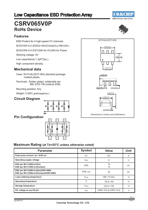
CSRV065V0PRoHs DeviceFeaturesESD Protect for 4 high-speed I/O channels. IEC61000-4-2 (ESD)±14kV(Contact),±18kV(Air). IEC61000-4-4 (FET)20A for I/O,80A for Power. Working voltage: 5VLow capacitance:1.3pF(Typ.). High component density.Mechanical dataCase: SC70-6L(SOT-363) standard package, molded plastic.Terminals: Solder plated, solderable per MIL-STD-750,method 2026. Mounting position: Any Weight: 0.0091 gram(approx.).Pin ConfigurationCircuit DiagramkV kV V A 1866.5ESD V DC I PP ESD _VDD °C °C 260 ( 10 sec)-55 to +125-55 to +85T SOL T j Lead soldering temperature Operating temperature ESD per IEC 61000-4-2(Air)Operating supply voltage Peak pulse current ( tp = 8/20 us)ParameterSymbolValueUnitMaximum Rating (at T A =25°C unless otherwise noted)ESD per IEC 61000-4-2(Contact)ESD per IEC 61000-4-2(Air)(VDD-GND)ESD per IEC 61000-4-2(Contact)(VDD-GND)Storage temperature DC voltage at any I/O pinT STG V IO(GND -0.5) to (VDD +0.5)3014°C VV5V RWM Reverse leakage current Reverse stand-Off voltage ParameterConditionsSymbol Min Typ Max UnitV RWM = 5 V, Pin 5 to Pin 2Pin 5 to Pin 2Electrical Characteristics (at T A =25°C unless otherwise noted)V PIN 5 = 5 V, V PIN 2 =0V ,V IO = 0~5V I RDiode breakdown voltage I R = 1 mA, Pin 5 to Pin 2uAV BD Forward voltageI F = 15 mA, Pin 2 to Pin 5V FV 1Clamping voltageI PP = 5 A, tp=8/20us,Any Channel Pin to GroundV CVIEC 61000-4-2 +6kV,Contact mode Any Channel Pin to Ground IEC 61000-4-2 +6kV,Contact moed VDD Pin to Ground9912.58.10.86Junction capacitanceV pin5 = 5V,V pin2= 0V, V IO =2.5V,f = 1MHz,Any Channel Pin to GroundC j 1.3pF1.6V pin5 = 5V,V pin2= 0V, V IO =2.5V f = 1MHz,Between Channel Pins 0.120.14V pin5 = 5V,V pin2= 0V, V IN =2.5Vf = 1MHz,Channel_x pin to ground - channel_y pin to ground0.050.07591VRATING AND CHARACTERISTIC CURVES (CSRV065V0P)% o f R a t e d p o w e r o r I P PAmbient temperature (°C)Fig. 1 - Power derating curveC l a m p i n g v o l t a g e ( V )Peak pulse current (A)0 4.5Fig. 2 - Clamping voltage vs. Peak pulse currentF o r w a r d v o l t a g e (V )Peak pulse current(A)Fig.3 - Forward voltage v.s. forward currentInput voltage (V)I n p u t c a p a c i t a n c e (p F )Fig.4 - Typical variation of C IN v.s. VIN01005025125751501020304050607080901001105.05.56.06.57.07.511112109876543204.55.05.56.06.57.07.54.03.53.02.52.01.51.00.50543210.00.20.40.60.81.01.21.41.61.82.0I n p u t c a p a c i t a n c e (p F )20Temperature (°C)Fig. 5 - Typical variation of C IN v.s. temperatureFig. 6 - Transmission line pulsing (TLP) measurement1.008040100601201.051.101.151.201.251.301.351.401.451.50T r a n s m i s s i o n l i n e p u l s i n g (T L P )c u r r e n t (A )Transmission line pulsing(TLP)voltage(V)01356247818141210864216T r a n s m i s s i o n l i n e p u l s i n g (T L P )c u r r e n t (A )Transmission line pulsing(TLP)voltage(V)Fig.7 -Transmission line pulsing (TLP) measurement001356910181412108642162478End W 1Reel Taping SpecificationSC70-6L (SOT-363)SC70-6L (SOT-363)BCdDD 2D 1SYMBOLA(mm)(inch)1.969 MIN.2.20 ± 0.102.40 ± 0.104.00 ± 0.101.55 ± 0.103.50 ± 0.051.75 ± 0.1050.0 MIN.13.0 ± 0.201.35 ± 0.104.00 ± 0.102.00 ± 0.058.00 ± 0.3014.4 MAX.178 ± 10.094 ± 0.0040.087 ± 0.0040.053 ± 0.0040.061 ± 0.0047.008 ± 0.0400.512 ± 0.008SYMBOL(mm)(inch)0.315 0.012±0.138 ± 0.0020.069 ± 0.0040.157 ± 0.0040.157 ± 0.0040.079 ± 0.0020.567 MAXEFPP 0P 1WW 1C05 = Device code X = Date Code Y = Control CodeSuggested PAD LayoutSIZE(inch)0.031(mm)0.800.351.300.0140.051SC70-6L(SOT-363)1.940.076E2.740.108B C D AMarking CodePart Number CSRV065V0PMarking CodeC05XYC05XY.123654Standard PackageCase Type Qty per Reel(Pcs)3000SC70-6L(SOT-363)Reel Size (inch)7。
PIC16C72A-I/SOPIC16F677-I/SS(密脚)PIC16F870-I/SPPIC16F886-I/SOPIC16F886-I/STPIC18F46K20-E/PTPIC18F6520-I/PTPT1301PT1301RF2126SD2200DLPISMA5102STG8203STK0460FSTPR1020CTSTPR1620CTTEA5767TIP49TIP49W19B320SBT9(代替型号W19B320ABT7H)2SA1266-Y2SA933AD7524JNZAP1507A T89C51RD2BS2F7HZ0194ABS2F7HZ07395CS5460-BSZDG211BDJEPM7064SLC44-10NEPM7064SLC44-10NK1118LPC2136FBD64MAX6103EURMJE5731AGMP2601MP7720MP7720MP7722MP7782PIC12C672-I/SNR5402N101KDREF3030AIDBZREF3030AIDBZS9013S9013S9015S9015SB8100SN74LS595NSTC89C55RD+40C-P TL3842TL3842TLC2543CNTLC2543CNTLC549CPTN2124K1TYN267PTYN267PX5045PZ48637407805080508050805080508050855085508550855085508550SB2401N40071N4747A-G1N4748A-G24M晶振2N90C2SD4662SN36324128BWP6N1366N13674LV59578L0578L05AD524ARAD524ARAK4645AMS1117-3.3V BC807DM-25-7 BH6799FVM-TR BS108BSM15GP120-B2 C8051F330DCA T1025JI-30CA T6219-33CR2LS-30DNY380PNDPA1870DPA423G DSPIC30F2010 DSPIC30F4012 ES1DESD5B50ST1G FAN2011EMPX FQPF8N60CG3JGBPC3508W GBU8DGTM900BHCF4201M013TR HER308HER308HMC287MS8HV9931LGIC7107IP101AIR2520DIRF730IRF740IRF830IRF840ISL9R1560PF2J2-Q06B-GKBU6JKBU8JLM1086-3.3VLM2576-5VLM4040AIM3-5.0LP3966ET-ADJLT1013LT1085CM-33M25P64-VMF6TP M88C200MAX3072EESA MBR1040MBR2045MBR30100CT MBR30100PTMC33981BPNAMP1029EM-LF-Z MP1029EM-LF-Z MP1410ES-LF-Z MP1482MP1488MP1488DJ-LF-Z MP1519DQLMP1540MP1580HS-LF-Z MP1953DN-LF-Z MP2105DJ-LF-Z MP2259MP2481MP2602DQ-LF-Z MP3202DJ-LF-Z MP3202DJ-LF-Z MUR820GMUR860GMUR860GNCP1014ST100T3G OP290GPCF2128PIC10F204T-I/OT PIC10F206T-I/OT PIC12C508-04/P PIC12F629-I/PPIC12LC509APIC16C72A-I/SO PIC16F688-I/SL PIC16F883-I/SO PIC16F886-I/SO PIC18F4680-I/P PIC18F46K20-E/MLPS1010RPS106RPS12046PS12046PT2256RL207(国产/进口)S20C40S80833CNUASAK-C504-2E24 SKRBAAE010 SKRBAAE010SLA7026MSLA7026MSLA7033SMAJ150ASP1110SP3232BEASS32STP2NK100ZSTP2NK90ZT6316ATD62003APTDA7396TNY278PNTNY278PNTOP222YTOP222YTPS71533DCKRTWH8751UAA3595HN/C3UC3844UF306ULN2803AGUTC3308VIPER53ZS3051212085S29AL016D70TF1010 2N30552N40332N62462SC26252SC26252SC40832SK1334BYTL-E2SK14112SK2334ST60EPF06PBF60EPF06PBF75333P7MBP75JB060-01A2611DAE2501BAME8800BEETYAME8800MEETZAN7815AP3700ZTR-E1B0530WS-7-FBC141BCR1AM-12ABL182LBQ24070BS170BSM15GP120-B2BTA2112-600BBTA2112-600BCP2102CS4344CZZCS8900AIQ32/CQ32 CXA2075DB3E2023ECWV1334KC9ED03EMD812EMP812FM1072LPFMQ-G5GSFS3KM-10AFS5KM-10AGS3J-BGT50J101HT2015-PLHT9032CHWD2109IHLP2525C2EBR47M01 IHLP2525C2EBR47M01 IP101A-LFIRF9140NIRFU9024NIRL2203NIRLML6401J2-005B-GK4M51323PC-DG75 K4M51323PC-DG75 k4s561632h-uc60K9G8G08KBpc25005-gKDT1304KSB1151YL6569L6569L6599DLA7213LA7213LD7550LM4853MMLMC7101AIMLP2985-18DBVR LT1615LTF5022T-3R3N2R5 MASWSS0115 MBR0530MBR2545PTMBR2545PT MBRB2045CTMC3403PMCP2551T-I/SN MCP9800MJE172MJE172MJE172MJE182MP1518DMP1583DSMP1593MP2259MP2363MP2363MSP430F223IRHAR MUR440NDC7002N-NCopa348a1dckrPCM1772PWG4PESD3V3L1BApi2259PIC12F509PIC16C433/JWPIC16F688-I/STPIC16G630-I/PPIC18F2420-I/MLPIC18F4321-I/PTR1114Q331r1130h001c-t1R3112N251ARE200BRGP30JRSOP36230TRS6A0073X01-C0CXS812C33S87C752-5A18S87C752-5A28SC0603C220M05SKN2000/03SLF6028T-4R7M1R6-PEsn74ahc1g00dcksn74lv1g06dckSPHE8202Lss14SST39VF6401B-70-4C-EKE STP140NF75STP140NF75STP40NF10STP40NS15STP8NF55-06STPS2060CTSTPS20S100STRX6757STTA3006PTA8440TDA7266PTDA8560QTDA8560QTDA8571JTDA8920BJTEA1761TTG35C60THX208TIC246MTLV1117-33CDCYRG3 TM9926TM9926FSTN6R04-H-ETOP200YATPA8920BTHTPA8920THTPS62000DGSTRLML2502TSC2003TSOP36230TRTSOP36230TRTWH8778UC3573NUC3573NUR5596VI-JW2-CZWM8731YDS-305YPPD-J001YPPD-J014AYPPD-J014BYPPD-J015BYPPD-J016BZTX65112-215SYGC-S530-E1/TR8 19-217/S2C-AM2N2VY/3T 25LC040T-I/SNAMC7150BA T54S-7-FBZX84C6V8LT1CA T809FDC6000NZFHP3130IS5XFHP3230IMU8XFUSE-5AHER207IP4035CX24IP4041CX25IRLM6401TRPBFIRLMS2002TRPBFLMH6639MF/NOPBLTC1872ES6LTC1872ES6MBR0520LT1GMBR0520LT1GMBRA210LT3GMCP1702T-3302E/CB MSP430F2111IPWRPT4115S-80930CLMCSB240SP6201EM5-L-3.3/TRSP6201EM5-L-ADJ/TR SP6205TPS61030RSATVP5146PFPTVP5146PFP10V 1500UF16V 3300UF19-217-R6C-AM2P1VY-3T 2MI100F-0252MI50S-0502SC19706.3V 1500UF6.3V 2200UF6.3V 3300UF6N1376N1376N13774HC138D74HC245D7MBR50NF060A TMEGA48V-10PUBTA12-600BCS9803GPD304XF20U40DNFDFS6N754-NLFODM121R2IN5822KA5M0765RQCTUMBR20H200CMCF5212CAE66PA42PIC12F683-I/SNPIC16C57C-04/PPIC16F677-I/SOPIC24FJ256GA110-I/PT PM15CMA060SC9803GPSIA0903X01SKD31F/16SKD31F/16SSG8205ASTP4NM60TIP41CTL494CVUB60-16N0116F74-I/P1NC452N602SD16102SK26112SK26112SK28372SK283739SF020A-70-440TPS125420(压力传感器)5651(压力传感器)5652(压力传感器)5L0380R67F110(温控开关)67F110(温控开关)6MBI50S-12074HCT540DB75333PADF-2-1ADF-2-1ADF-2-1ADNS-2610(传感器)AI325AMC7135AMC7135A T90PWM3-16SQA T90SC7272CA TMEGA128-16AUA TMEGA128-16AUBC182BBC212BBCR8PM-14LABL8553-33PRMBS2F7HZ0194ABS2F7VZ0194-BS2F7VZ7395 BSM50GB120DN2BSM50GB120DN2BSM50GB120DN2BT169BTA140-800BTA140-800C1815C945CP10TD1-24ACP157D1-24ACSC9270D1D40D304XD304XDS12C887DS12C887DS52502DSPIC30F3013-30I/SOE13007F12C20CFDS6898AZFJA13009TUFQPF10N60CFQPF6N80CFS450R17KE3FS450R17KE3FS8205AFS8205AGU1GHEF4069UBPHT2015-LQHT2015-LQHWD4863HWD809ICL7612DCPAICL7612DCPAIN4764AIN4764AIN4764AIP4035CX24IP4041CX25IRF7750TRIRF9540NIRF9540NIRFZ24IW1692K3113KA4558SL6565L6565LC863324A-5S68LC863528C-55LOLM1237BDKC/NA LM311PLM317BTLP2981ATM5-3.0LT1249CN8LT6233MB6SMBR10H200MBR20100MBR2045CTGMC33262PMCP4023T-103E/CH MCP4922-E/PMCP9800AOT-M/OTG MCR100-6MCR100-6MFRC500MGSF1N03LT1G MOC3061MP1411DH-LF-Z MPX5010DPNR12S5/500PCM2900EGPIC12F683-I/PPIC16F877A-I/LPM30CTJ060-36PSD35/16RB521G-30RB521S-300.075RT8008-18RBRT8008-18RBS29GL032N90TFI030 SBL1545CTSD0418ASISG6849-65DSG6849-65DSKKT250/14ESKKT250/14ESKR71/16SP1110SP1117-1.8SP2110SSG50C60SSG50C60STP6NK60STPR1620CTSTPS3045CWSTRF6652STRF6652STRF6652TA2003PGTA2003PGTAP476K016SCTDA9886TSTHC63LVDF84B THX202TOP254YNTOP254YNU1560VIPER12ASWFF7N60WFF7N60XC2S100-5TQ144C YDS205YPPD-J015BYPPD-J018E05NL03LA178487-120N60S520N60S52DI300A-050D2SC50472SC50473P4MH403CNQ1004921QP1018AAA T3155ITP-T1AM9945NAO4803AAPT5010LVRAXK5F26547AXK6F26547BA V70LT1GCBC3225T100KR CBC3225T220KRCD3610CS9803GPDAC712UKEL817CEPM3256AQC208-10N EPM3256AQC208-10N ERA-1FDV303NFDV303NFSDL0165RNFSDM311FSDM311FSUSB30MUXGL827HA17358HD4066BHN27C101AG-15IR2520DIR2520DIR2520DIRF1045IRF2805IRF3805IRFB4227PBFIRFB4227PBFJM20316K4M51323PC-DG75 KA78T12TUL6563L6599DLD7575PSMC3PHACVPEMI1320MI1321MOC3063MST726C-LFNDC7002NNTJD2152PT1G NTJD2152PT1GPIC10F200TPIC18F242-I/SP PMWD20XNPS22056RM600DY-66SS6A0073X14-COCX SMAJ6.0ASN75LBC174NST330C16COST330C16COSTB10NB50STB10NB50STP12NM50FPSTP9NK50ZSTPS1L40ASTTH2L06STW20N60TC4011BFTC4451VPATCM809JENB713 TDA7439DSTDA7439DSTFBS4650-TR3 TFBS4650-TR3TL082CDTTL084CNTNY266PNTOP244YNTS3USB221DRCRG4 TSC2003VU034-18N01YDS512YDS512YPPD-J001AZ0103MNZ0103MN901316F872-I/SP16F872-I/SP16F873A16F873A2MBI200N-0602SK26116MBP75RS1206MBP75RS12074HC59574LS244A940AM9945NAM9945NA TA5428CM0565RCM0565REL817EPM570GT144C4 EPM570GT144C4 FS9922GWS6967IRF460KA5H0380RYTU LD7575LM117KLM358LM385B12LP2950ACZ-3.3G LP2950ACZ-3.3G MP2259DJ-LF-Z MP2359MUR3060PTNCP1575NCP1653APG/ADR PS21246-EPS21255-EPT4105CRHRP8120S8550SBC337SBC337-25SKIIP31NAB12T16 SLA6026SN75LBC174NSR160TB1334FBTB1334FGTOP254YNTOP255YNUC3842BW5100WFP50N062SA812M62SA812M72SB6242SB772P2SC1623L62SC1623L72SC2712GR2SC3356R242SC3356R252SC3357RE2SC3357RF2SC4226R242SC4226R252SD772P2SD882P74LVCH162245ADL 74LVCH162245ADL 74LVCH16245ADL A1156-YA1156-YA1270-YA1270-YAA T3155AD8300ANAOT430B560CBAS21DW-7FS7M0880TU GBPC3508HIT647-EQHIT667-EQHTC78L05KA1L0380RBTU KA1L0380RBTU KBJ406KBJ410KBJ410KRC1055KSP10BUKST10MFTLC863328A-5T46LC863328A-5T46LTC3406ES5LTV350QV-F04M430V138TNE555NPMBT4401PMBT4403PS2501-1-A-KKPS2501L-1-E3-A-KK/L QM30HC-2HSKR240/16THX202HTJM4558CDTTLP281-4YG225N471061.5KE13CA1D600A-0301D600A-0301N47331N474424AA64-I/SN24AA64-I/SN28SF040A65HVD308267L09003466D115A-0506D115A-05074LVC14APW74LVC14APW75645P82C55AD7846JPADM705ARZAM188ES-20KCAO4842LAPW7060KC-TRL BYV26EBYV26EC945CH372ADAC0830LCWM DAC8412FPCEPM3032ALC44-10 EPM7128ELCES6628FFDS6912FDS6912HER153HER153HWP2171IR2103IS62C256AL-45 ISR154-600JW1FSN-DC12V JW2SN-DC12VKA3525ADKSB772KSB772YKSB772YKTB2955-O-UKTB2955-O-ULM318LM714M50195M50195M50195MAX7129ACPL MC145102PMC145102PMC33204DMCPS08AW16CFU MPX5100DPMT88E43BSMX26L6420MC NRF24L01PA92PIC16F630T-I/ST/SL PT7A6632JSAB80C537SARS01V01SG5841DZSII9013CLUSII9030CTUSPD03N60C3STP6NK60ZFPSTS2300SSTS2301STS2307TCD1304DGTCD1304DGTLP114TP3465TPC8107VLA517VLA517W27E010-702SC3320A04842LBYV27-200D17P149CTD20LC40D92-03MUR110RLMUR3040NCP1207PNW6005ASPIC24FJ64GA002-I/ML SP6013ASTB36NF06T2-1T-KK81TL494CNTPS79101DBRUC3842BN2SD1781KT146R74HC595DBCR3KM-12RAHEF4066BPL7905LM324NMDC100A1600VMIC29302BTSCN-3-28SN75176BPTLC7528CNYG225C2YG225N4YG255N215V-D12061N414825LC1282N22222N22222N29073656AG3DD15D6CWQ06FN6CWQ06FNA3120A3120AD7863BR-10AD8531ART-REELADM705-ARZAPXA200ARA220MF55G A T89S52-24JUA T89S52-24JUBAS16BTS660PE3180ABU9431-C1CD1206-S01575CL6012XCL6012XEL817B-SFM24C04A-GFQU13N10LFQU13N10LFR107FR107GL827HER307IRF5305IRS2168DJ174J174J175J175J175K9F2G08R0A-JIBOKIA431AKIA431BKSD1691L358L358LM3845MMMAX3072MAX491CPDMBT35200MMBTA44-400V-300mA MP1482MP1482OV9650-KL1APC929PIC16CE625-04/SOPT70302S6A0073X14-COCXS6A0073X14-COCXS6A0073X14-COCX SAB82352HSARS01V1SF5408SH3750ASH3750ASLA7026MSMAJ4735ASMAJ4744ASR3100STM32F103VETSTP10NK70ZFPTHX203HTL431TL594CDRTL594CDRTPS5430DDAG4TPS72301DBVRUF1004CTUF1004CTUGSP08JXC3S1000-4FT256I1N457A1N938B-1JANTX2068DD2SA812M62SA812M72SB772P2SC1623L62SC1623L72SC2712GR2SC33552SC3356R252SC4226R242SC4226R252SD882P455E5L0380R830BA2624A3901A3901SEJTR-TA T17C128BA6220BF247BBJ8P153ABJ8P153ABJ8P508ABJ8P508ABQ2054BSM100GD120DLC BSM100GD120DLC BTVZ0502SABZT52C10-7C8051F120CD3620CD4067CD4067CS3310CS3310DAN202KDAN202KDP104CDS2433DS2433DTB114ESDTC144EKADTC144EKADTC343TSEL817BEL818CEM78P153SEM78P156ELEM78P156ELEM78P156NEM78P156NEM78P447SEM78P447SEM78P458AEM78P458AEM78P803A/BEN25F40-100GCPEN25F80EV1527FHP3230IM8XGBU25AGRM55ER72A475KA01L HCPL2530HCPL-2531.SHIT647-EQHIT667-EQHT1380HT1381HT1620HT1621HT1621BHT1621GHT7130HT7130HT7133HT7133HT7136HT7136HT7144HT7144HT7150HT7150HT7530HT7530HT7533HT7533HT7536HT7536HT7544HT7544HT7550HT7550HWD2171HY5DU121622CTP-D43-C ICP-N38ISS86ISS86ISS86J174J174J175J175J176J176J177J177JCS830CKRA105MKSP2222KST10MTFKTC9014CL78L05AC2LG9110LM2575T-5LM324LM324LM3475MFLM3485MMLM3658SDLM4562NALM567CHLNK501PNLTC5505-1ES5MAX491CPDMAX706CSA-TMC145010DWMC145010PMC145012DWMC145012PMC145018PMC56F8323VFBEMCP1726-1202E/SNMCP2030-I/SLMJL4281AGML4803MLC3100AMMBT5401MP1410ES-LF-Z MP1411OV2610PAN3101PIC18LF4682-I/PT PMBT4401PMBT4403PP25-48-15PTFA192001ERV4145ANS5C-225HVSA9259SAB80C166-MSB10100FCTSD2200DLPISM2845SS8050CBUTB2132FNTB2132FNTB62705FNTC9274N-011TJM4558CDTTLC5510AITM9936TOP210TV00570002CDGB VIPER53DIP-E WM8768GEDS WM8768GEDS 7805780678087809781278157824790579067908790979127924130031300574HC0474HC13874HC16474HC24574HC59578M0578M0678M0878M0978M1278M15A940A T1628/AM1628 B772BD242CBD243CBD244CBT131-600BT134-600EBT136-600EBT137-600BT137-600EBT138-600EBT151-500RBT151-500RBT152-500RBT169DBTA06BTA08BTA12BTA16BTA26BTA41BTB04-600SL BU406C106DC2073CD40106CD4011CD4011CD4052CD4053CD4066CD4541BNCD6282CD6283CD9088CS4334CT502D880D882E13001AE13005AE13005AE13005AE13007AE13007AEV1527FM62429GT2300/2301/2302 GT3400/GT3401 GT4953GT8205GT9435GT9926HT1380HT1621BHT1628HT6221HT6222JRC4558DKA3525KA3842KA3842/UC3842 KA3843KA3845KA7500KA7805KA7806KA7808KA7809KA7812KA7815LM2575LM2575T/SLM2576LM2576T/SLM258LM2596LM2596T/SLM2901LM2901LM2902LM2902LM2903LM2903LM317MLM317TLM324LM324NLM339LM339NLM358LM358NLM393LM393NLM567MAC97A6/8MCR100-6MCR100-8MUR1660CTNE555POP07PL2303PT2262PT2272TDA2003TDA2030ATDA2030ATDA2822M/(6-15V) TEA2025B/(9-15V) TIP122TIP127TIP31CTIP32CTIP41CTIP42CTL494TYN612UC3843UC3845ULN2003ULN2803UTC2003LUTC339X0405MFX0605MFZ0103MFZ0607MF0802A字符LCD液晶显示模块0802B字符点阵模块12232-4液晶模块12232-9中文3V液晶显示模块12232A液晶模块12232B图型点阵模块12232C点阵模块128128图型显示模块12864A图型显示模块12864A液晶12864C图型点阵模块12864C中文点阵模块12864I低功耗汉字显示液晶模块12864T液晶模块/LCM模块/液晶屏(图) 12864点阵图型液晶模块T6963C1601A大字符显示模块1601字符显示模块1601字符液晶模块1602大字符点阵显示模块19264A蓝白/黄绿液晶模块19264A蓝白液晶显示模块19264B图型点阵液晶显示模块2×10中文字库液晶显示模块240128-1显示模块240128A蓝白模块240128A液晶显示模块240128点阵液晶模块240128中文字库点阵显示模块/液晶屏24064A图型液晶/LCM模块2864I-1中文点阵液晶模块/LCM模组3.5寸液晶显示屏320240C图型点阵模块3V低功耗0802A字符模块3V低功耗字符点阵3V图型点阵12832中文LCD3V图型点阵160128A显示模块4.3寸夏普彩屏4004A字符液晶模块402A两行大字符模块COG240128C低功耗模块LCD/LCM12864-1液晶显示模块LCD/LCM240128-1点阵图型模块LCD/LCM5.7寸320240A高亮液晶LCD/LCM液晶404ALCD/LCM英文液晶显示模块LCD12232-2液晶模块LCD12832A显示模块LCD12864-06模块LCD12864-07模块LCD128645显示模块LCD12864D液晶显示模块LCD12864J字库模块LCD1601A点阵字符模块LCD1601字符显示模块LCD1602大字符显示模块LCD1604液晶模组LCD大字符1601显示模块LCD点阵显示模块12232-1LCD液晶LCD液晶模块LCD液晶显示模块LCD液晶显示模块128641LCM12864-7点阵显示模块LCM161点阵模块LCM192641点阵图型模块T6963C控制芯片液晶12864F串口中文两行液晶模块/3V显示屏串口字库/图型LCD液晶显示模块低功耗12232F中文图型点阵显示模块(图) 低功耗液晶显示模块两行字符点阵模块三星LTV350QV-F04显示湿度计LCD液晶液晶12232-3显示模块液晶屏3.5寸带触模液晶显示240128A模块字符162液晶显示模块字符204点阵显示模块字符点阵0801B模块字符模块2002A点阵40021N40071N4744A1N581925AA1024-I/SM2SC1946455EADM705-ARZBSM100GD120DLC BSM100GD120DLC BTA20BTA204S-600D BTVZ0502SACM75YE13-12FCM75YE13-12F DAC0832LCNDS2433DS2433DSA17-16AESM6045DVESM6045DVEV1527FDC37C78-HTGBU25AHC08HC08HER204HER204ICP-N38IMBH75D-060S IRLZ44AIRLZ44AISS86ISS86ISS86J174J174J175J175J176J176J177J177KRA105MLM2575T-5.0LM2576T-ADJLM2576T-ADJLM2595S-ADJLM2595S-ADJLM2596T-ADJLM2596T-ADJLM567CHLP8345CLD-1.8 LS14LS14MAX491CPD MAX491CPD MCP2030-I/SL MP2365DN-LF-Z NCP1014ST65T3G NS0013LFP4KE51AP4KE51AP4KE51APL2303HXPL2303HXPL2303HXPL2303HXPL2303HXPL2305PL2305POS-100PS12036PS12036PT76S16ART9164CMS3C2410ALS3C2410ALSA8281IGSA8282SAB80C166-MSB10100FCTSB2040FCTSB2040FCTSD2405APISM0038SPHE8202RQSPIF225A-HL231 SS26T3GSS26T3GSS26T3GST6368B1/FEMST6368B1/FEM STC352TA2132TA2132TB2132FNTB2132FNTB62705FNTL494CNTMG8E60UM3750AVIPER53DIP-EWM8522GWM8768GEDSWM8768GEDS YDS212YDS21278057809130011300320100160L2C43A16V/680UF22UH24C0229GL512N11TAI010 2KDB08M2SA1349/2SC3381 2SD1835S2SD1835S-AA2SK1172SK1173224G-1-100E3314R-1-203E400V/10UF4921QP1002B4921QP1009A4921QP1017A4921QP1043B4921QP1043C4921QP1046A4921QP1047A74HC16475NF7578L0578L0578L088202TAD620ARAD8620BRADTL2-18AP4313KTRBD9703FP-E2BD9703FP-E2BL8023BL8506-42CSMBN/53SBS170CM2020-00TRCP10CS3310-KPD1555DB107DM0465RYDTUDS1620DSPIC30F4013EM78P152ANEN25F40-100GCPFDN340PFF501FM1105GBLC03GBLC03HER207HMMC3124HMMC3124HY5DU1216DTP-D43-C IN5819INA106UINA128UINA128UAISD2560PITR8307/S18ITR8307/S18 ITR9909J112J112JRC4558JZ6206(3.3V) JZ9261(5.0V)K3435KA378R12KA7500KA7500KBP204GKBP204GKBP206GKBP208LAN9115-MT LM2575T-5LM324LM339LM358LM386LM393LM94021BIMG LT11293LTC3703EGM27C512-12F1 M81C55A-2 MAX232MAX3221EEAE MBI1802MC34064A MDSR-7 MDSR-7MIC2951-02YM MP1517DR-LF MT1389QE-K NE555OP27FZOPA2132OPA2604PC817PS21867RJ23N3ABOPT RK3055ERTL8102ELS29GL064A90TFIR4S3P9234XZZ-COC4S3P9234XZZ-COC4S8261AAJS8261AANS8261ABPS8261ABZS9013HSA8281SA8281SPHE8202RQ/TQSPW20N60S5SST89E516RD-40-C-PIE SSU2N60BSTPS2045CTTDA2822(6V)TEA2025(9V)TL431(+-0.5%)TL431ATL494TL494TSOP2136UC3842UDZ5V6BUSBN9603-28MVIPER12AVIPER22AXC1736EPC103653-1103653-120JL2C20JL2C6MBI20GS-0606MBI20GS-06074HCT14D93C46AAH180-WG-7A T89S51-24AU/AIA TMEGA48V-10MUA TMEGA48V-20AUA TMEGA48V-20AUA TMEGA8-16AUA TMEGA8-16AUA TMEGA8-8AUA TMEGA8-8AUCA T1025JI-30CA T1025WICD1691CBCD1691CBCD1691CBCD74ACT20MCMQ82C55AZCMQ82C55AZCS9803GPD71055GBD71055GBEPM3256AQC208-10N FM24CL16-GFM24CL16-GFM24CL16-GFM25L256BGGP30MGP30MHCF4017BEYHCF4017BEYHCF4060BMHCF4060BMHMC284HMC484HMC574MS8ETRHV9931ISP2032A80LT48ISP2032A80LT48KIA7806APKIA7806APLM8V302LM8V302LMX2531LQ1778 LTC3200-5LTC3200-5LTC3200-5M29W128FH70N6E MAX942MBRM140TMBRM140TMBRM140TMC1413BDGMC1413BDGMC68SEC811E2FN MC68SEC811E2FN MIG15J503HMIG30J501LMIG30J503LMP7731DF-LF-Z MT6225ANCP1395APGNJU9202BMNTJD4401NT1ON4742P06P03LVGP6KE24APLS-2PS11035PS11035QS3257QS3257R3111H481C-T1-F SAB80C537NSAB80C537NSN74HC74QPWRQ1 SP3232ESPX1117M3VC0568-V33-LF YPPD-J016BYPPD-J016E13009130091N458A24BC022SB6492SD6693296W-1-1013296W-1-20274HC14N74HC245N74HC37388W8010-NNB188W8510H-BAN1 88W8510H-BAN1 89C2051-12PUAH1802-WG-7AH180-WG-7AM29LV040B-60RJI BN/54SCD4529BECS4334DG442DYZDG442DYZDSE130-06AEM78P468NBQJ HCPL2530IN5817IN5817IN5817IN5820IRF7105IRS2186STRPBF KRC231SM27C512-10F1 MAX610CPANJM0302NJM0302NJM13700MNJW0281NJW0281NL17SZ74USPCF8574PPS1010RSRC4558IDRSB240SGH80N60UFDSI3018-F-FSRSR260TAS3204PAGTDA7535TJM4558CDTTL7705ACPTOP257YN13005MD2.0V稳压管2.0V稳压管2SA20942SC2712GR2SK27172SK3483-Z2SK38784921QP1023A4921QP1023A500欧可调电阻500欧可调电阻6MBP100RD060-01 6MBP100RD060-01 8302(HX3021)AD620ANA T29C512-12JCAU6331BA V99BC847BBC847BBC847BBUL38DBUL38DBUL58DBUL58DBUT11AC8051F023C945GCM2020-00TREN25F16ESD5B5.0ST1G FQPF5N80FQPF6N80FS3KM-10AFSBB20CH60FSBB20CH60 FSCM0765RGWDTU FSQ100FZT751FZT751HX3001(打LTWK) IKP20N60IRAMX16UP60A-2 IRFR120J5027-R(1.5A)J5027-R(2A)J5027-R(3A)KA3525AL149VL149VL6561/L6562LM556CMLMC555MA4820MC33179MCP1603T-180I/OS MCP1700T-5100/MB MCP6002-I/PMCP6002-I/PMP7782MPSA92MPSA92MS621FE-FL11EOV2640PC816PIC16F628APMBT4401/4403PS229QTF53BR1224N102H-TR-FR1224N102H-TR-F RFD16N05LRPS-2-30RY5W-KRY5W-KS29GL064A90TFIR40 SB20150FCTSI4425BDY-T1-E3SI4425BDY-T1-E3 SIA0903X01STA540SASTRX6757TC77-3.3MCTTR TDA2009TDA7266PTDA7266PTDA7266SATDA7375TDA7375TDA7377TDA7497TDA7497TDA7499TDA7499TJM4558CDTTLP521-3TMPZ84C011BF-8 TMPZ84C011BF-8TP0610K-T1-E3TP0610K-T1-E3TP0610K-T1-E3TP2808HCNTSF2N60MTVP5160U2352BU2352BUMB3NUMB3NUMB3NUMH3NUMH3NVR61F1250107N60S508-0559-0308-0559-0308-0559-03103308-611N120CND160NQ0825LC010AT-I/OT29F040-70LC2SA12202SC28902SC31332SC31332SD5532SJ19874LS53388E1011SA5-RCJ1C000 AC712AC712AD7711ARAHC164AO4828AOD442A T90SC7272CBC549CBCW72BTA41-700BBU406BW-S15W2+BW-S15W2+CM100DY-24HCM100DY-24HCM100DY-24HCNA30C101M-TMCS43L21-CNDSPIC30F6011A-30I/PT EEE2AA100UPFBC40LCFM1702SLGS-R51212HY5DU121622DTP-D43-C IR2161IR2161IR2161IR2161IR2161IRF3205IRFB17N50LIRKT105-16IRKT105-16IRS2186ISL9N312AD3ISO124PISO124PLM1086-3.3VLM224JLM318NLM3916NLM3916NLM3S615-IQN50LPC2132FBD64MBI1802MBR20100MC14093BCPMJ15003MJ15003MP1591DNMP1591DNMP1591DNMP1593DNMP1593DNMP1951DNMP3302DJ-LF-ZMRF166WMRF166WOM02OV9655PHE840MA6100MA04R17 RCV420AGRV5C348A-E2SD0418ASSKKT91/12ETA8127ATC77-5.0MCTTRTC77-5.0MCTTRTEA1098TVTM1618ATMS320LF2406APZA TNY254PUDN2983AUDN2983AV A7205CFWRA2412CS-1WWRA2412CS-3W1300513007130071300713009201002020025103.5251005472490001100UF/100V100UF/100V100UF/1W100UF/25V100UF/450V100UF/450V100UF/50V10UF/25V11-MD12716F887-I/P16V2200UF16v470uf173977-51N54081N5819218S4PASABG22UF/25V25N1202A233J2SC380-O2SC380-O2SD6492SD6692SK3485-Z-E2X80-DR230-S+35V1000UF4.3,1W4.3,1W40CPQ10040CPQ100470UF/100V47UF/16V47或,33UH68UF/400V6KA2474ALVC164245DGG 74LCX16245MTD 7914G-1-000E7914G-1-000E8N609N90A29L160ATV-70F ACT30BAD594ADAD7710ARZAD7710ARZAD8551ARAD8551ARAD8551ARAD96685TQAMC7150DLFTAMC7150DLFTAPM2301AR2001A T24C1024BA TMEGA8-8PUA TMLU810.46D.1,27G6346A AU6371AXK860145WGB1403NBA V23SBCM8011A2KPFBL8551BSM150GT120DN2BSM150GT120DN2BU52011HFVBUP314BUP314DC1815CD4514CM2020-00TRCP10TD1-24ACSC9270CSC9270CX4060CXD2498R13003DD313DF30FC-24DP-04VDFLS220L-7-FDS188B20DS1991C-FS+DSPIC30F3013-30I/SO DSPIC30F3013-30I/SODTV32DDTV32FEPM7128AELC84-10NEPM7128AELC84-10NER1004CTFMLG16SFMLG16SFMS6363CSXFP-20-1,27-60FPQ-100-0.5-10A FPQ-44-0.8-1G FQI16N60CFS10ASJ-2FSD210FSDL0165RNFT2232FTD2017G6K-2F-RF GBU8JGWS7301EHB9500HS108NHX3021ICX282AQINIC-1611LIR21592IR21592IR2233JIR2233JIRAMX16UP60A IRAMX20UP60A IRF014NPBF IRF014NPBF IRF014NPBF IRFP450IRFS9N60APBF IRFU320。
Very Low Power CMOS SRAM 32K X 8 bitBS62LV256Pb-Free and Green package materials are compliant to RoHSn FEATURESŸ Wide V CC operation voltage : 2.4V ~ 5.5V Ÿ Very low power consumption :V CC = 3.0V Operation current : 25mA (Max.) at 70ns 1mA (Max.) at 1MHz Standby current : 0.01uA(Typ.) at 25O C V CC = 5.0V Operation current : 40mA (Max.) at 55ns 2mA (Max.) at 1MHz Standby current : 0.4uA (Typ.) at 25O C Ÿ High speed access time : -55 55ns(Max.) at V CC : 4.5~5.5V -70 70ns(Max.) at V CC : 3.0~5.5V Ÿ Automatic power down when chip is deselected Ÿ Easy expansion with CE and OE options Ÿ Three state outputs and TTL compatible Ÿ Fully static operation Ÿ Data retention supply voltage as low as 1.5V n DESCRIPTIONThe BS62LV256 is a high performance, very low power CMOS Static Random Access Memory organized as 32,768 by 8 bits and operates form a wide range of 2.4V to 5.5V supply voltage.Advanced CMOS technology and circuit techniques provide both high speed and low power features with typical CMOS standby current of 0.01uA and maximum access time of 70ns in 3.0V operation.Easy memory expansion is provided by an active LOW chip enable (CE), and active LOW output enable (OE) and three-state output drivers.The BS62LV256 has an automatic power down feature, reducing the power consumption significantly when chip is deselected.The BS62LV256 is available in DICE form, JEDEC standard 28 pin 330mil Plastic SOP , 600mil Plastic DIP , 8mmx13.4mm TSOP (normal type).n POWER CONSUMPTIONPOWER DISSIPATIONSTANDBY(I CCSB1, Max)Operating(I CC , Max)V CC =5.0V V CC =3.0V PRODUCT FAMILYOPERATING TEMPERATUREV CC =5.0V V CC =3.0V1MHz10MHzf Max. 1MHz10MHzf Max.PKG TYPEBS62LV256DCDICE BS62LV256PC PDIP-28 BS62LV256SC SOP-28 BS62LV256TC Commercial +0O C to +70O C4.0uA0.4uA1.5mA18mA35mA0.8mA12mA20mATSOP-28 BS62LV256PI PDIP-28 BS62LV256SI SOP-28 BS62LV256TIIndustrial -40O C to +85O C5.0uA0.7uA2mA20mA40mA1mA15mA25mATSOP-28n PIN CONFIGURATIONSn BLOCK DIAGRAMBrilliance Semiconductor, Inc. reserves the right to change products and specifications without notice.A14A12A7A6A5A4A3A2A1A0DQ0DQ1DQ2GNDn PIN DESCRIPTIONSn TRUTH TABLENOTES: H means V IH; L means V IL; X means don’t care (Must be V IH or V IL state) n ABSOLUTE MAXIMUM RATINGS (1)SYMBOL PARAMETER RATING UNITSV TERM Terminal Voltage withRespect to GND-0.5(2) to 7.0 VT BIAS Temperature UnderBias-40 to +125 O CT STG Storage Temperature -60 to +150 O CP T Power Dissipation 1.0 WI OUT DC Output Current 20 mA1. Stresses greater than those listed under ABSOLUTE MAXIMUM RATINGS may cause permanent damage to the device. This is a stress rating only and functional operation of the device at these or any other conditions above those indicated in the operational sections of this specification is not implied. Exposure to absolute maximum rating conditions for extended periods may affect reliability.2. –2.0V in case of AC pulse width less than 30 ns. n OPERATING RANGERANGAMBIENTTEMPERATUREV CC Commercial 0O C to + 70O C 2.4V ~ 5.5VIndustrial -40O C to + 85O C 2.4V ~ 5.5Vn CAPACITANCE (1) (T A = 25O C, f = 1.0MHz) SYMBOL PAMAMETER CONDITIONS MAX. UNITSC INInputCapacitanceV IN = 0V 6 pFC IOInput/OutputCapacitanceV I/O = 0V 8 pF1. This parameter is guaranteed and not 100% tested.n DC ELECTRICAL CHARACTERISTICS (T A = -40OC to +85OC)A 2. Undershoot: -1.0V in case of pulse width less than 20 ns. 3. Overshoot: V CC +1.0V in case of pulse width less than 20 ns.MAX RC.5. I CC (MAX.) is 20mA/35mA at V CC =3.0V/5.0V and T A =70O C. 6. I CCSB1(MAX.) is 0.4uA/4.0uA at V CC =3.0V/5.0V and T A =70O C.n DATA RETENTION CHARACTERISTICS (T A = -40O C to +85OC)CC A 2. t RC = Read Cycle Time.3. I CCDR(Max.) is 0.4uA at T A =70O C.n LOW V CC DATA RETENTION WAVEFORM (CE Controlled)Data Retention ModeV CCt CDRV CCt RV IHV IHCE ≧V CC - 0.2VV DR ≧1.5VCEV CCn AC TEST CONDITIONS (Test Load and Input/Output Reference)Input Pulse Levels Vcc / 0V Input Rise and Fall Times 1V/ns Input and Output TimingReference Level0.5Vcct CLZ , t OLZ , t CHZ , t OHZ , t WHZC L = 5pF+1TTL Output LoadOthersC L = 100pF+1TTL1. Including jig and scope capacitance.n KEY TO SWITCHING WAVEFORMSn AC ELECTRICAL CHARACTERISTICS (T A = -40O C to +85OC)READ CYCLECYCLE TIME : 55ns (V CC = 4.5~5.5V) CYCLE TIME : 70ns (V CC = 3.0~5.5V) JEDEC PARAMETERNAMEPARANETERNAMEDESCRIPTIONMIN. TYP . MAX. MIN. TYP . MAX. UNITS t AVAX t RC Read Cycle Time 55 -- -- 70 -- -- ns t AVQX t AA Address Access Time -- -- 55 -- -- 70 ns t E1LQV t ACS Chip Select Access Time -- -- 55 -- -- 70 ns t GLQV t OE Output Enable to Output Valid -- -- 25 -- -- 35 ns t E1LQX t CLZ Chip Select to Output Low Z 10 -- -- 10 -- -- ns t GLQX t OLZ Output Enable to Output Low Z 10 -- -- 10 -- -- ns t E1HQZ t CHZ Chip Select to Output High Z -- -- 30 -- -- 35 ns t GHQZ t OHZ Output Enable to Output High Z -- -- 25 -- -- 30 ns t AVQXt OHData Hold from Address Change10----10----ns1 TTL ALL INPUT PULSES → ← 90% V CC GND Rise Time : 1V/ns Fall Time : 1V/ns 90% → ← 10%10%n SWITCHING WAVEFORMS (READ CYCLE)READ CYCLE 1 (1,2,4)READ CYCLE 2 (1,3,4)READ CYCLE 3 (1, 4)NOTES:1. WE is high in read Cycle.2. Device is continuously selected when CE = V IL .3. Address valid prior to or coincident with CE transition low.4. OE = V IL .5. Transition is measured ± 500mV from steady state with C L = 5pF. The parameter is guaranteed but not 100% tested.D OUT CED OUT CE OE ADDRESS t RC t OHt AA D OUT ADDRESS t OHn AC ELECTRICAL CHARACTERISTICS (T A = -40OC to +85OC)WRITE CYCLEn SWITCHING WAVEFORMS (WRITE CYCLE)WRITE CYCLE 1 (1)t WCt WR(3)t CW(11)t WP(2)t AWt OHZ(4,10)t AS t DHt DWD IND OUTWECEOEADDRESS(5)WRITE CYCLE 2 (1,6)NOTES:1. WE must be high during address transitions.2. The internal write time of the memory is defined by the overlap of CE and WE low. All signals must be active to initiate a write and any one signal can terminate a write by going inactive. The data input setup and hold timing should be referenced to the second transition edge of the signal that terminates the write.3. t WR is measured from the earlier of CE or WE going high at the end of write cycle.4. During this period, DQ pins are in the output state so that the input signals of opposite phase to the outputs must not be applied.5. If the CE low transition occurs simultaneously with the WE low transitions or after the WE transition, output remain in a high impedance state.6. OE is continuously low (OE = V IL ).7. D OUT is the same phase of write data of this write cycle. 8. D OUT is the read data of next address.9. If CE is low during this period, DQ pins are in the output state. Then the data input signals of opposite phase to the outputs must not be applied to them. 10. T ransition is measured ± 500mV from steady state with C L = 5pF. The parameter is guaranteed but not 100% tested. 11. t CW is measured from the later of CE going low to the end of write.D IN D OUT WE CE ADDRESSn ORDERING INFORMATIONNote:BSI (Brilliance Semiconductor Inc.) assumes no responsibility for the application or use of any product or circuit described herein. BSI does not authorize its products for use as critical components in any application in which the failure of the BSI product may be expected to result in significant injury or death, including life-support systems and critical medical instruments.n PACKAGE DIMENSIONSθSOP - 28n PACKAGE DIMENSIONS (continued)11428150.004 ~ 0.006 0.004 ~ 0.008 0.0045±0.0026 0.0315±0.004 0.0197 0.022±0.004 0.008±0.001 0°~ 8°0.004 Max. 0.528±0.0080.315±0.004 0.465±0.004 0.009±0.002 0.039±0.002 0.0433±0.004 INCH c1 L1 0 y D E HD L e SYMBOLc A A1 b A2 b1 UNIT0.10 ~ 0.16 0.80±0.10 0°~ 8°0.1 Max. 0.55±0.10 11.80±0.10 0.50 13.40±0.208.00±0.10 - 0.004+0.008- 0.10+0.20 0.115±0.065 MM0.10 ~ 0.21 0.20±0.03 0.22±0.05 1.00±0.05 1.10±0.10 TSOP - 28SECTION A-A12°(2x)PDIP - 28n Revision HistoryRevision No. History Draft Date Remark2.4 Add Icc1 characteristic parameter Jan. 13, 20062.5 Change I-grade operation temperature range May. 25, 2006- from –25O C to –40O C2.6 Revised I CCSB1 sepc. Sep. 05, 2006- from 1.0uA to 4.0uA for 5V C-grade- from 2.0uA to 5.0uA for 5V I-grade- from 0.2uA to 0.4uA for 3V C-grade- from 0.4uA to 0.7uA for 3V I-gradeRevised I CCDR sepc.- from 0.2uA to 0.4uA for C-grade- from 0.4uA to 0.7uA for I-grade。
ICSI reserves the right to make changes to its products at any time without notice in order to improve design and supply the best possible product. We assume no responsibility for any errors which may appear in this publication. © Copyright 2000, Integrated Circuit Solution Inc.DESCRIPTIONThe 1+51 IS62LV1024L and IS62LV1024LL are low powerand low Vcc,131,072-word by 8-bit CMOS static RAMs. They are fabricated using 1+51's high-performance CMOS technol-ogy. This highly reliable process coupled with innovative circuit design techniques, yields higher performance and low power consumption devices.When CE1 is HIGH or CE2 is LOW (deselected), the device assumes a standby mode at which the power dissipation can be reduced by using CMOS input levels.Easy memory expansion is provided by using two Chip Enable inputs, CE1 and CE2. The active LOW Write Enable (WE )controls both writing and reading of the memory.The IS62LV1024L and IS62LV1024LL are available in 32-pin 8*20mm TSOP-1, 8*13.4mm TSOP-1, 450mil SOP and 48-pin 6*8mm T.-BGA.CMOS STATIC RAM.EATURESAccess times of 45, 55, and 70 ns Low active power: 60 mW (typical)Low standby power: 15 µW (typical) CMOS standbyLow data retention voltage: 2V (min.) Available in Low Power (-L) and Ultra Low Power (-LL)Output Enable (OE ) and two Chip Enable (CE1 and CE2) inputs for ease in applications TTL compatible inputs and outputs Single 2.7V to 3.6V power supplyIS62LV1024L/LL1234567891011121314151632313029282726252423222120191817NC A16A14A12A7A6A5A4A3A2A1A0I/O0I/O1I/O2GNDVCC A15CE2WE A13A8A9A11OE A10CE1I/O7I/O6I/O5I/O4I/O3PIN CON.IGURATION32-Pin SOPPIN DESCRIPTIONSA0-A16Address Inputs CE1Chip Enable 1 Input CE2Chip Enable 2 Input OE Output Enable Input WE Write Enable Input I/O0-I/O7Input/OutputC o C onnectionVcc Power GNDGroundPIN CON.IGURATION32-Pin 8x20mm TSOP-1 and 8x13.4mm TSOP-1OPERATING RANGERangeAmbient TemperatureV CCCommercial 0°C to +70°C 2.7V to 3.6V Industrial40°C to +85°C2.7V to3.6V48-Pin 6x8mm T.-BGAIS62LV1024L/LLABSOLUTE MAXIMUM RATINGS (1)Symbol ParameterValueUnit V TERM Terminal Voltage with Respect to GND 0.5 to Vcc + 0.5V V CC Vcc related to GND0.3 to +4.6V T BIAS Temperature Under Bias 40 to +85°C T STG Storage Temperature 65 to +150°C P TPower Dissipation0.7WNotes:1.Stress greater than those listed under ABSOLUTE MAXIMUM RATINGS may cause permanent damage to the device. This is a stress rating only and functional operation of the device at these or any other conditions above those indicated in the operational sections of this specification is not implied. Exposure to absolute maximum rating conditions for extended periods may affect reliability.CAPACITANCE (1,2)Symbol Parameter Conditions Max.Unit C IN Input Capacitance V IN = 0V 6p.C OUTOutput CapacitanceV OUT = 0V8p.Notes:1.Tested initially and after any design or process changes that may affect these parameters.2.Test conditions: T A = 25°C, f = 1 MHz, Vcc =3.0V.DC ELECTRICAL CHARACTERISTICS (Over Operating Range)Symbol ParameterTest ConditionsMin.Max.Unit V OH Output HIGH Voltage V CC = Min., I OH = 1.0 mA 2.2 V V OL Output LOW Voltage V CC = Min., I OL = 2.1 mA0.4V V IH Input HIGH Voltage 2.2V CC + 0.3V V IL Input LOW Voltage 0.30.4V I LI Input Leakage GND ≤ V IN ≤ V CC 11µA I LOOutput LeakageGND ≤ V OUT ≤ V CC11µANotes:1.V IL = 3.0V for pulse width less than 10 ns.TRUTH TABLEModeWE CE1CE2OE I/O Operation Vcc Current Not Selected X H X X High-Z I SB , I SB (Power-down)X X L X High-Z I SB , I SB Output Disabled H L H H High-Z I CC Read H L H L D OUT I CC WriteLLHXD INI CCIS62LV1024L/LLIS62LV1024L POWER SUPPLY CHARACTERISTICS(1)(Over Operating Range)-45L ns-55L ns-70L ns Symbol Parameter Test Conditions Min.Max.Min.Max.Min.Max.Unit I CC Vcc Dynamic Operating V CC = Max., CE = V IL Com. 40 35 30mASupply Current I OUT = 0 mA, f = f MAX Ind. 45 40 35I SB TTL Standby Current V CC = Max.,Com. 0.3 0.3 0.3mA(TTL Inputs)V IN = V IH or V IL, CE1≥ V IH Ind. 0.4 0.4 0.4or CE2 ≤ V IL, f = 0I SB CMOS Standby V CC = Max., f = 0Com. 50 50 50µACurrent (CMOS Inputs)CE1≥ V CC 0.2V,Ind. 75 75 75CE2 ≤ 0.2V,or V IN≥ V CC 0.2V, V IN≤ 0.2VNote:1.At f = f MAX, address and data inputs are cycling at the maximum frequency, f = 0 means no input lines change.IS62LV1024LL POWER SUPPLY CHARACTERISTICS(1)(Over Operating Range)-45LL ns-55LL ns-70LL ns Symbol Parameter Test Conditions Min.Max.Min.Max.Min.Max.Unit I CC Vcc Dynamic Operating V CC = Max., CE = V IL Com. 40 35 30mASupply Current I OUT = 0 mA, f = f MAX Ind. 45 40 35I SB TTL Standby Current V CC = Max.,Com. 0.2 0.2 0.2mA(TTL Inputs)V IN = V IH or V IL, CE1≥ V IH Ind. 0.3 0.3 0.3or CE2 ≤ V IL, f = 0I SB CMOS Standby V CC = Max., f = 0Com. 5 5 5µACurrent (CMOS Inputs)CE1≥ V CC 0.2V,Ind. 10 10 10CE2 ≤ 0.2V,or V IN≥ V CC 0.2V, V IN≤ 0.2VNote:1.At f = f MAX, address and data inputs are cycling at the maximum frequency, f = 0 means no input lines change.IS62LV1024L/LLREAD CYCLE SWITCHING CHARACTERISTICS(1)(Over Operating Range)-45-55-70Symbol Parameter Min.Max.Min.Max.Min.Max.Unit t RC Read Cycle Time45 55 70 ns t AA Address Access Time 45 55 70ns t OHA Output Hold Time10 10 10 ns t ACE CE1 Access Time 45 55 70ns t ACE CE2 Access Time 45 55 70ns t DOE OE Access Time 20 25 35ns t LZOE OE to Low-Z Output0 5 5 ns t HZOE OE to High-Z Output015020025ns t LZCE CE1 to Low-Z Output5 7 10 ns t LZCE CE2 to Low-Z Output5 7 10 ns t HZCE CE1 or CE2 to High-Z Output015020025ns Notes:1.Test conditions assume signal transition times of 5 ns or less, timing reference levels of 1.5V, input pulse levels of 0.4V to2.2Vand output loading specified in .igure 1.2.Tested with the load in .igure 2. Transition is measured ±500 mV from steady-state voltage. Not 100% tested.AC TEST CONDITIONSParameter UnitInput Pulse Level0.4V to 2.2VInput Rise and .all Times 5 nsInput and Output Timing 1.5Vand Reference LevelOutput Load See .igures 1AC TEST LOADS.igure 1..igure 2.IS62LV1024L/LLNotes:1.WE is HIGH for a Read Cycle.2.The device is continuously selected. OE , CE1 = V IL , CE2 = V IH .3.Address is valid prior to or coincident with CE1 LOW and CE2 HIGH transitions.(1,3)AC WAVE.ORMS (1,2)IS62LV1024L/LLWRITE CYCLE SWITCHING CHARACTERISTICS (1,3) (Over Operating Range, Standard and LowPower)-45-55-70SymbolParameter Min.Max.Min.Max.Min.Max.Unit t WC Write Cycle Time 45 55 70 ns t SCE CE1 to Write End 35 50 60 ns t SCE CE2 to Write End35 50 60 ns t AW Address Setup Time to Write End 35 50 60 ns t HA Address Hold from Write End 0 0 0 ns t SA Address Setup Time 0 0 0 ns t PWE " WE Pulse Width 35 40 55 ns t SD Data Setup to Write End 25 25 30 ns t HDData Hold from Write End0 0 0 ns t HZWE WE LOW to High-Z Output 15 20025ns t LZWE WE HIGH to Low-Z Output555nsNotes:1.Test conditions assume signal transition times of 5 ns or less, timing reference levels of 1.5V, input pulse levels of 0.4V to2.2V and output loading specified in .igure 1.2.Tested with the load in .igure 2. Transition is measured ±500 mV from steady-state voltage. Not 100% tested.3.The internal write time is defined by the overlap of CE1 LOW, CE2 HIGH and WE LOW. All signals must be in valid states to initiate a Write, but any one can go inactive to terminate the Write. The Data Input Setup and Hold timing are referenced to the rising or falling edge of the signal that terminates the Write.4.Tested with OE HIGH.AC WAVE.ORMSWRITE CYCLE NO. 1 (9- Controlled)(1,2)IS62LV1024L/LLWRITE CYCLE NO. 2 (+- , CE2 Controlled)(1,2)1.The internal write time is defined by the overlap of CE1 LOW, CE2 HIGH and WE LOW. All signals must be in valid states to initiate a Write, but any one can go inactive to terminate the Write. The Data Input Setup and Hold timing are referenced to the rising or falling edge of the signal that terminates the Write.2.I/O will assume the High-Z state if OE = V IH .DATA RETENTION SWITCHING CHARACTERISTICSSymbolParameterTest ConditionMin.Max.Unit V DRVcc for Data Retention See Data Retention Waveform 2.0 3.6V I DRData Retention CurrentVcc = 2.0V, CE1 ≥ Vcc 0.2VCom. (-L) 30µA Com. (-LL) 5µA Ind. (-L)50µA Ind. (-LL)10µA t SDR Data Retention Setup Time See Data Retention Waveform 0ns t RDRRecovery TimeSee Data Retention Waveformt RCnsDATA RETENTION WAVE.ORM (+- Controlled)IS62LV1024L/LLDATA RETENTION WAVE.ORM (CE2 Controlled)IS62LV1024LORDERING IN.ORMATION Commercial Range: 0°C to +70°C Speed (ns)Order Part No.Package45IS62LV1024L-45Q450mil SOPIS62LV1024L-45T8*20mm TSOP-1IS62LV1024L-45H8*13.4mm TSOP-1IS62LV1024L-45B6*8mm T.-BGA 55IS62LV1024L-55Q450mil SOPIS62LV1024L-55T8*20mm TSOP-1IS62LV1024L-55H8*13.4mm TSOP-1IS62LV1024L-55B6*8mm T.-BGA 70IS62LV1024L-70Q450mil SOPIS62LV1024L-70T8*20mm TSOP-1IS62LV1024L-70H8*13.4mm TSOP-1IS62LV1024L-70B6*8mm T.-BGA IS62LV1024LORDERING IN.ORMATION Industrial Range: 40°C to +85°C Speed (ns)Order Part No.Package45IS62LV1024L-45QI450mil SOPIS62LV1024L-45TI8*20mm TSOP-1IS62LV1024L-45HI8*13.4mm TSOP-1IS62LV1024L-45BI6*8mm T.-BGA 55IS62LV1024L-55QI450mil SOPIS62LV1024L-55TI8*20mm TSOP-1IS62LV1024L-55HI8*13.4mm TSOP-1IS62LV1024L-55BI6*8mm T.-BGA 70IS62LV1024L-70QI450mil SOPIS62LV1024L-70TI8*20mm TSOP-1IS62LV1024L-70HI8*13.4mm TSOP-1IS62LV1024L-70BI6*8mm T.-BGAIS62LV1024L/LLIntegrated Circuit Solution Inc.HEADQUARTER:NO.2, TECHNOLOGY RD. V, SCIENCE-BASED INDUSTRIAL PARK,HSIN-CHU, TAIWAN, R.O.C.TEL: 886-3-5780333.ax: 886-3-5783000BRANCH O..ICE:7., NO. 106, SEC. 1, HSIN-TAI 5TH ROAD,HSICHIH TAIPEI COUNTY, TAIWAN, R.O.C.TEL: 886-2-26962140.AX: 886-2-26962252IS62LV1024LLORDERING IN.ORMATIONCommercial Range: 0°C to +70°CSpeed (ns) Order Part No.Package 45IS62LV1024LL-45Q 450mil SOPIS62LV1024LL-45T 8*20mm TSOP-1IS62LV1024LL-45H 8*13.4mm TSOP-1IS62LV1024LL-45B 6*8mm T.-BGA 55IS62LV1024LL-55Q 450mil SOPIS62LV1024LL-55T 8*20mm TSOP-1IS62LV1024LL-55H 8*13.4mm TSOP-1IS62LV1024LL-55B 6*8mm T.-BGA 70IS62LV1024LL-70Q 450mil SOPIS62LV1024LL-70T 8*20mm TSOP-1IS62LV1024LL-70H 8*13.4mm TSOP-1IS62LV1024LL-70B6*8mm T.-BGAIS62LV1024LLORDERING IN.ORMATIONIndustrial Range: 40°C to +85°CSpeed (ns) Order Part No.Package 45IS62LV1024LL-45QI 450mil SOPIS62LV1024LL-45TI 8*20mm TSOP-1IS62LV1024LL-45HI 8*13.4mm TSOP-1IS62LV1024LL-45BI 6*8mm T.-BGA 55IS62LV1024LL-55QI 450mil SOPIS62LV1024LL-55TI 8*20mm TSOP-1IS62LV1024LL-55HI 8*13.4mm TSOP-1IS62LV1024LL-55BI 6*8mm T.-BGA 70IS62LV1024LL-70QI 450mil SOPIS62LV1024LL-70TI 8*20mm TSOP-1IS62LV1024LL-70HI 8*13.4mm TSOP-1IS62LV1024LL-70BI6*8mm T.-BGA。