EClamp2122S
USB Downstream Port Filter & TVS
For EMI Filtering and ESD Protection
PROTECTION PRODUCTS - EMIClamp ?Description
Features
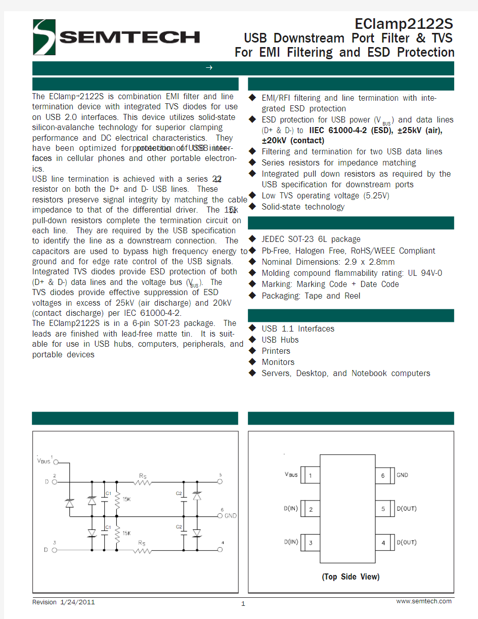
Circuit Diagram Pin Configuration
Applications
Mechanical Characteristics
JEDEC SOT-23 6L package
Pb-Free, Halogen Free, RoHS/WEEE Compliant Nominal Dimensions: 2.9 x 2.8mm
Molding compound flammability rating: UL 94V-0 Marking: Marking Code + Date Code Packaging: Tape and Reel
The EClamp ?2122S is combination EMI filter and line termination device with integrated TVS diodes for use on USB 2.0 interfaces. This device utilizes solid-state silicon-avalanche technology for superior clamping performance and DC electrical characteristics. They
have been optimized for protection of USB inter-protection of USB inter-faces faces in cellular phones and other portable electron-ics.
USB line termination is achieved with a series 22Ωresistor on both the D+ and D- USB lines. These
resistors preserve signal integrity by matching the cable impedance to that of the differential driver. The 15k Ωpull-down resistors complete the termination circuit on each line. They are required by the USB specification to identify the line as a downstream connection. The capacitors are used to bypass high frequency energy to ground and for edge rate control of the USB signals.Integrated TVS diodes provide ESD protection of both (D+ & D-) data lines and the voltage bus (V BUS ). The TVS diodes provide effective suppression of ESD voltages in excess of 25kV (air discharge) and 20kV (contact discharge) per IEC 61000-4-2.
The EClamp2122S is in a 6-pin SOT-23 package. The leads are finished with lead-free matte tin. It is suit-able for use in USB hubs, computers, peripherals, and portable devices
USB 1.1 Interfaces USB Hubs Printers Monitors
Servers, Desktop, and Notebook computers
EMI/RFI filtering and line termination with inte-grated ESD protection
ESD protection for USB power (V BUS ) and data lines (D+ & D-) to IIEC 61000-4-2 (ESD), ±25kV (air),±20kV (contact)
Filtering and termination for two USB data lines Series resistors for impedance matching
Integrated pull down resistors as required by the USB specification for downstream ports Low TVS operating voltage (5.25V) Solid-state technology
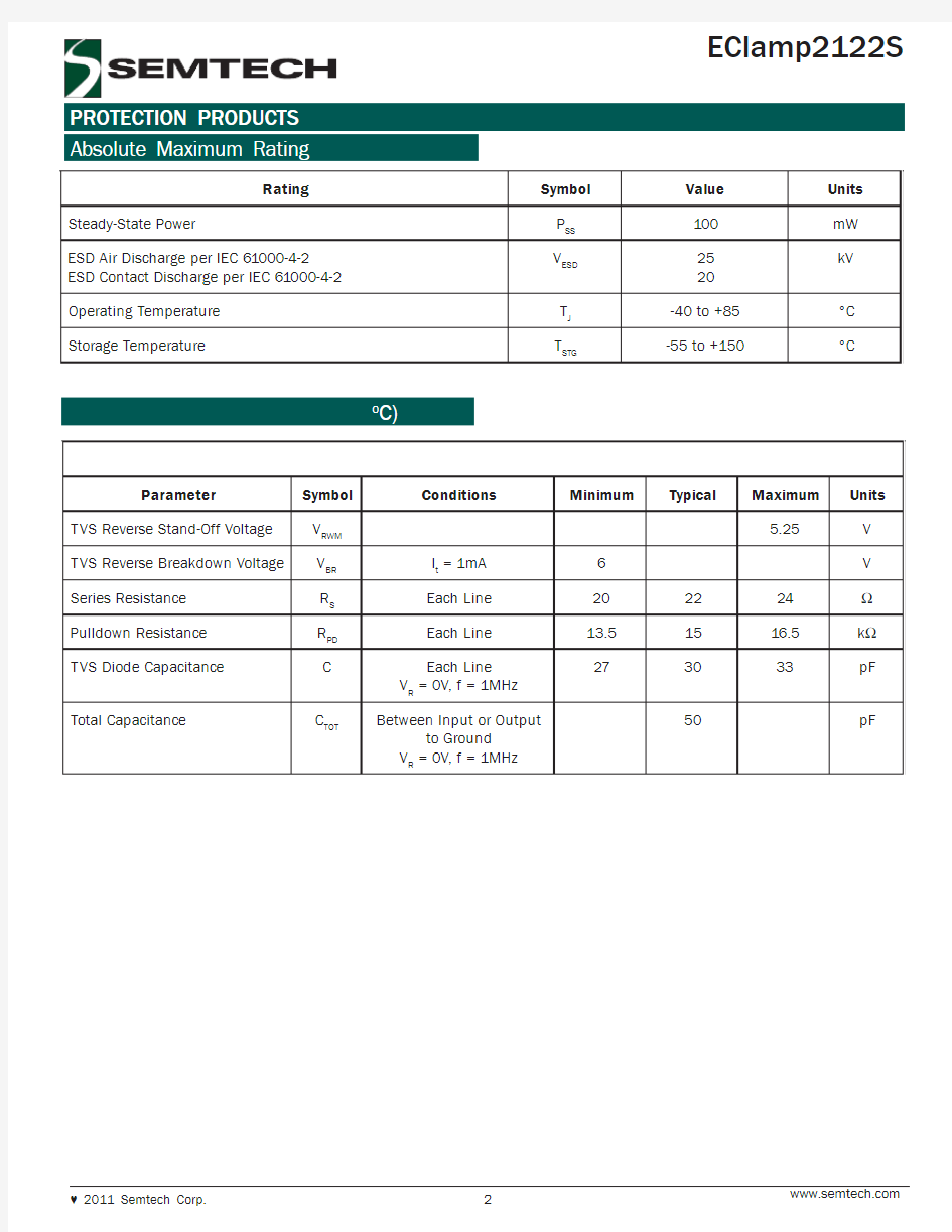
Absolute Maximum Rating
g
n i t a R l o b m y S e u l a V s t i n U r
e w o P e t a t S -y d a e t S P S S 001W m 2
-4-00016C E I r e p e g r a h c s i D r i A D S E 2-4-00016C E I r e p e g r a h c s i D t c a t n o C D S E V D S E 5202V k e r u t a r e p m e T g n i t a r e p O T J 58+o t 04-C °e
r u t a r e p m e T e g a r o t S T G
T S 0
51+o t 55-C
°r
e t e m a r a P l o b m y S s n o i t i d n o C m u m i n i M l a c i p y T m u m i x a M s t i n U e g a t l o V
f f O -d n a t S e s r e v e R S V T V M W R 5
2.5V e g a t l o V n w o d k a e r B e s r e v e R S V T V R B I t A m 1=6V
e c n a t s i s e R s e i r e S R S e n i L h c a E 022242Ωe c n a t s i s e R n w o d l l u P R D P e n i L h c a E 5.31515.61k Ωe c n a t i c a p a C e d o i D S V T C e n i L h c a E V R z H M 1=
f ,V 0=7
2033
3F p e
c n a t i c a p a C l a t o T C T
O T t
u p t u O r o t u p n I n e e w t e B d n u o r G o t V R z
H M 1=f ,V 0=0
5F
p Electrical Characteristics (T = 25o C)
Typical Characteristics
ESD Clamping (Pin 4 or 5 to GND)(8kV Contact per IEC 61000-4-2)ESD Clamping (Pin 4 or 5 to GND)(-8kV Contact per IEC 61000-4-2)
Note: ESD data is taken with a 20dB attenuator ESD Clamping (Pin 1 to GND)(-8kV Contact per IEC 61000-4-2)
ESD Clamping (Pin 1 to GND)
(8kV Contact per IEC 61000-4-2)
Typical Insertion Loss S21
(Pin 2 to 5 with respect to GND)
Typical Insertion Loss S21
(Pin 3 to 4 with respect to GND)
Normalized Junction Capacitance
vs. Reverse Voltage (Data Pins)
0.0
0.10.20.30.40.50.60.70.80.91.01.11.21.31.41.50
1
23
4
5
Reverse Voltage - V R (V)
C J (V R ) / C J (V R =0
)
Applications Information
Figure 1 - EClam Figure 1 - EClamp2p2p2122S Cir 122S Cir 122S Circuit Diagram
cuit Diagram
Device Connection
The EClamp2122S is designed to provide termination,EMI filtering and ESD protection for two USB I/O lines.The equivalent circuit diagram is shown in Figure 1.The device is connected as follows:
z
USB data lines are routed through the
EClamp2122S for easy implementation and opti-mum pc board layout. Pin 1 is connected to the voltage supply line. The input of the D+ line is
routed into pin 2 and out of pin 5. The input of the D- line is connected at pin 3 and the output at pin 4. Pin 6 is connected to ground. The ground connection should be made directly to the ground plane for best results. The path length is kept as short as possible to reduce the effects of parasitic inductance in the board traces.
USB Port Design with EClamp2122S
The Universal Serial Bus (USB) specification requires termination and filtering components for proper opera-tion. In addition, an open USB socket is vulnerable to hazardous ESD discharges in excess of 15kV. These discharges can occur on the data lines or the voltage bus. The EClamp2122S is an easily implemented solution designed to meet the termination & EMI filter requirements of the USB specification revision 1.1. It also provides ESD protection to IEC https://www.doczj.com/doc/2d2119160.html,B line termination is achieved with series resistors on both the D+ and D- lines. These resistors preserve signal integrity by matching the cable impedance to that of the differential driver. 15k Ω pull-down resis-tors are used to identify a downstream port. Capaci-tors are used to bypass high frequency energy to ground and for edge rate control of the USB signals.Integrated TVS diodes provide ESD protection of both (D+ & D-) data lines and the voltage bus (V BUS ).General layout guidelines are given below:
z Avoid running D+ & D- signal line traces near high speed clock lines or similar signal lines.
z Avoid running critical signal lines near board edges.z Place the EClamp2122S near the USB connector to restrict transient coupling.
z
Minimize the path length between the USB connec-tor and the EClamp2122S.
Outline Drawing - SOT-23 6L
Contact Information
Semtech Corporation
Protection Products Division
200 Flynn Rd., Camarillo, CA 93012
Phone: (805)498-2111 FAX (805)498-3804
Tape and Reel Specification
Device Orientation in Tape
e p a T
h t d i W
)x a
M(,B D1
D E F
K
)X A
M(
P0
P2
P)X A
M(T W m
m
8
m
m
2.4
)5
61.(
m
m
1.0
+
5.1
m
m
0.0
-
m
m
0.1
5
0.0
±
01.±
5
7.1
m
m
5
0.0
±
5.3
m
m
m
m
4.2
1.0
±
0.4
m
m
1.0
±
0.4
m
m
5
0.0
±
0.2
m
m
m
m
4.0
m
m
0.8
m
m
3.0
+
m
m
1.0
-0
A0
B0
K
m
m
5
0.0-/+
3
2.3m
m
5
0.0-/+
71.3m
m
5
0.0-/+
73.1
User Direction of feed
YW = 2 - Alphanumeric characters for Date Code