Photoelectrical and Photovoltaic peroperties of n-ZnO/p-Si
Heterojunction
Xu Yanli, Li Jinhua*
Dept.of Electron Sience and tecnology, Changzhou University, Jiangsu 213164, China
*Communication author Email:jhli@https://www.doczj.com/doc/1518327159.html,
Abstract n-ZnO thin films doped In with 2 atm.% were deposited on p-type silicon wafer with textured surface by Ion Beam Enhanced Deposition method, after annealing and prepared front and back electrodes, the n-ZnO/p-Si heterojunction samples were fabricated. The photoelectric property of the sample were measured and compared with silicon solar cell. The result indicated the saturated photocurrent of n-ZnO/p-Si heterojunction was 20% greater than one of the Si solar cell. It means the ZnO/Si heterojunction has a higher ability of produce photoelectron then one of silicon solarcell. The result of the photovoltaic test of n-ZnO/p-Si heterojunction show The open circuit voltage and short-circuit current of the n-ZnO/p-Si heterojunction was 400mV and 5.5mA/cm2 respectively. It was much smaller than the one of silicon solar cells. The reason was discussed.
Key words: ZnO film; z-ZnO/p-Si heterojunction; Solar cell
1.Introduction
Zinc oxide(ZnO) is II-VI a attractive compound semiconductor with wide direct band gap of 3.37eV and large exciton binding energy of 60meV [1] at room temperature. ZnO thin flms has been extensively investigated due to its potential applications in blue and ultraviolet
light-emitting diodes,surface acoustic wave devices, solar cells, gassensors, varistors,etc [2~4]. When ZnO film was doped with the some metal atoms,such as Al, Sn, In, Ga etc the conductive properties will be increased[5-6]. Recently, quite a lot of research groups have devoted to fabrication of In doped or Al-doped ZnOfilms based p-n heterojunction combinded crystal silicon due to its potential applications in optoelectronic devices[7-10]. Because ZnO/Si heterojunction has different band-gap, reasonably, It could absorb from visible to ultraviolet light of sunlight in theory, consequently increases the conversion efficiency of the solar cells greatly. Besides, the ZnO/Si heterojunction solar cell have a number of potential advantages such as simple processing steps, and low processing temperatures[11].
In this study, the photoelectrcal and photoviltaic properties of n-ZnO/p-Si heterojunction will be introduced and comprared with crystal silicon solar cell.
2. Experiment
2.1 texture p-Si suface
Choosing (100) 3-inch silicon wafer with a resistivity of 3-8 ohm.cm, etched at 85o C for 18min in the 2% NaOH solution, cleaned and dying it. The p-type silicon wafer was
textured.
2.2 In doped ZnO film prepration
High purity (99.99% in purity) ZnO powder and In2O5 powders with an atom ratio of 2% were ball-milled,pressed and baked to prepare sputtering target. The Ion Beam Enhanced Deposition(IBED) was used to form the In doped n-ZnO film directely from the powder target. Concretely, the powder pressed targets were sputtered by Ar+ ions with an energy of 2.5 KeV and a beam current of 60mA, and In doped ZnO film was deposited on the p-Si substrat, the surface was textured. Before deposite, Ar+ bean of 50mA was used to sputter the substrate surface to etch the nature SiO2thin film. The substrate were placed on a round holder rotated with a speed of 2 rpm and the substrates also rotated with a speed of 12 rpm. All the films were was deposited for 6 hours. The thickness of the deposited films was about 0.5μm tested by α-step measurement.
2.3 Electrode formation
After annealing the ZnO/Si sample were printed silver plasm as the front electrode and sintered at 700o C for 10min in N2. Then evaporated Al film with a thickness of 0.3μm on the back as back electrode, metalized at 450o C, for 15min to get good ohm contact. n-ZnO/p-Si heterojunction solar cell was obtained. To comprare, a crystal silicon solar cell was fabricated with like process of surface texture and electrodes, phosphorus diffusion, but no anti-reflect laeyer of Si3N4 film.
3. Measurements
The shape of txtured surface was observed by microscope image analysis system , the thickness of ZnO thin films were tested by Dektak 150 profilometer and the crystal orientation was measured by XRD, the photoelectric property of the sample was measured by transistor characteristics tester, the photovoltaic property was tested by a solar cell measurement system. The crrier concentration was checked by Hall instrument.
4. Results and discussion
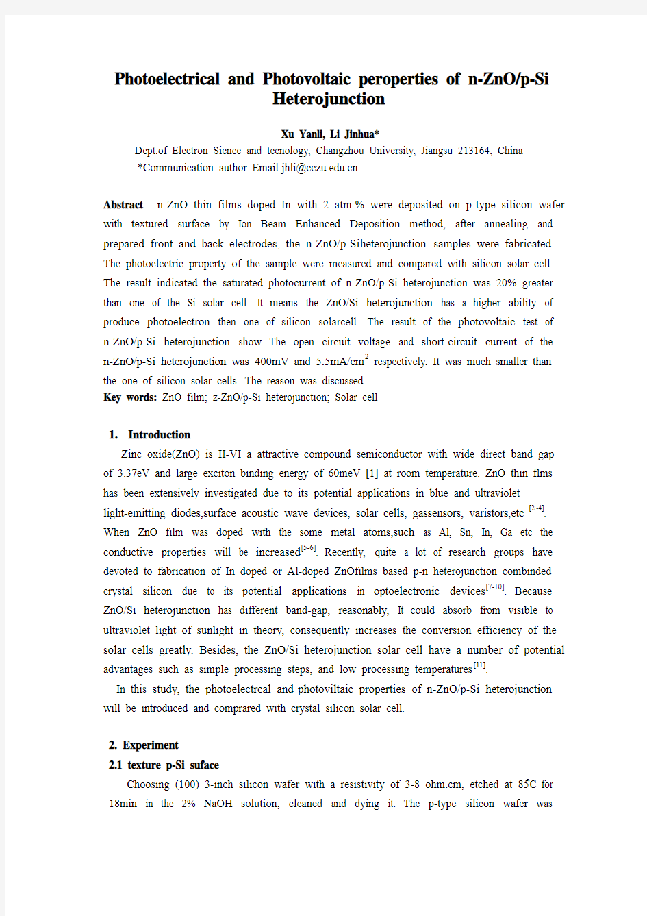
The surface shape of textured silicon wafer was shows as the Fig.1. it was observed the (100) orientation surface was very rough after the NaOH etching, It could increase the
Fig.1 Shape of the tex tured p (100) Si surface
2030405060 0
10k
20k
30k
40k
50k
60k
70k
80k
90k
(002)
annealed 550o C,3min
before annealing
Indium doped ZnO films
I
n
t
e
n
s
i
t
y
(
a
.
u
.
)
Two theta(deg)
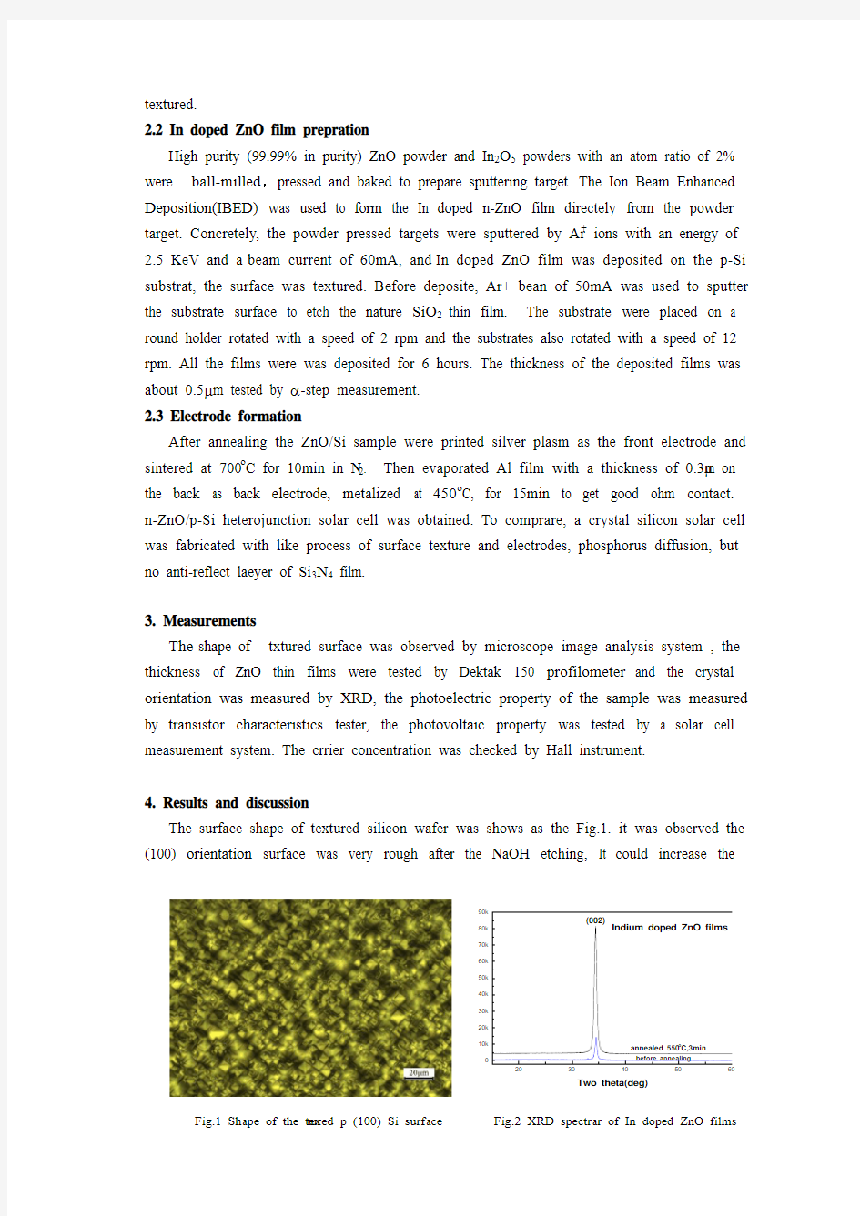
Fig.2 XRD spectrar of In doped ZnO films
effective surface area. Fig.2 was the XRD spectrar of the In doped ZnO films before and
after annealing. It has a single (002)c-axes orientation. Fig.3 was the Atomic Force photographs before and after annealed at 600oC for 5min in N 2. The roughness and grain size of the indium doped ZnO films were different. Fig.4 was a photograph of the n-ZnO/p-Si hetrojunction sample. Indium
doped
ZnO
films
were
characterized using Hall effect measurement by Van de Pauw method. Metal Indium was used as electrode of the Van de pauw figure. The results were listed in table1.
From the table 1 it could be seen that the sheet resistor, carrir mobility and carrir concentration
were
varied
with
the
temperature sensitively. Annealed at 600o C for 10min was the best codition.
It was choosed by n-ZnO/p-Si hetrojunction fabrication process.
The photoelectrical and photovoltaic properties of n-ZnO/p-Si heterojunction and Si solar cell were showed as Fig.5 and Fig.6 respectively.
The photocurrent and dark current were measured using a transister chanracterics tester and a white lamp of 60W, the irradiation energy density was about 4.2mW/cm 2. The photocurrent of the crystal silicon solar cell as compring was about 1.76mA/cm 2 at 2.0V . At the same conditions, the photocurrent of the n-ZnO/p-Si heterojunction was
Fig.3 AFM photograph of ZnO film
before(up) and after(down) annealing
Table 1 Hall effect measurement results of In doped ZnO films after annealing with different
Fig.4 a photograph of the n-ZnO/p-Si heterojunction sample
about 2.2mA/cm 2. it was more 20%higher than one of Si solar cell. But the dark current was larger than one of the Si cell(see Fig.5) and to make the photocurrent to saturation the supplied voltage was different. It was 0.5V and 1.8V respectively to silicon cell and heterojunction.The reasons suppose like folowing:
Because the bandgap of ZnO was aroud 3.37eV , wider than 1.13eV of Si, So heterojuntion sampl e could absorb the energy of ultraviolet light then produced more
photoelectrons, and these photoelectron all moved to the electrode helped by supplied voltage. It seems that to heterojuction the ability of produce photoelectron was higher than silicon solar cell. Needing higher voltage to reach saturation should be result in short excursion lengh of the photoelectron in the polycrystalline ZnO film with more defects, interface state and dangling valence bond.
The crystal silicon solar cell was self-made, it has not deposite Si 3N 4 film as anti-reflection film,and has not print thin assistant electrode. So the light-electrical conversion effectivity was aout 13.5%, the short current(Isc),open circuit voltage(V oc) was 22.75mA/cm 2, 0.635eV respectively under the standard irradiation. From Fig.6, to the z-ZnO/p-Si heterojunction, the V oc and Isc was about 5.5mA/cm 2,and 0.40V respectively. Why the photoelctron produce ability was higher than silicon cell but V oc and Isc was so lower than silicon cell? The reason bay be also due to the polycrystalline structure of ZnO. When test the photoelectrical property, some voltage was supplied on the both side of the p-n junction. All photoelectrons could get enough energy to get to the electrode, but when test photovoltaic property, without any electrcal surce supplied on the electrode, the defects, interface state, dangling in the ZnO film and interface will suppress or capture the photoelectron, make the excursion lengh short, thereby the V oc and Isc was evidently dicrease.
0.00.10.20.30.40.50.60.70.80.9 1.0
P h o t o c u r r e n t (m A )
photovoltage(V)
-15
-10
-5
5
10
15
20
C u r r e n t (m A )
Voltage(V)
Fig.5 Comprarision of photoelectrial propertity between ZnO/Si heterojunction and Si solar cell
Fig.5 Comprarision of photovoltaic propertity between ZnO/Si heterojunction and Si solar cell
5. Conclusion
The n-ZnO/p-Si heterojunction was fabricated by IBED tecnology and solar cell process.The photelectrical and photovoltaic property were measured and compared with crystal silicon solar cell. The results of photoelectrical test indicated that the saturation photocurrent of n-ZnO/p-Si hetrojunction was mor 20% higher than one of the silicon cell. It means the ZnO/Si heterojunction has a higher ability of produce photoelectron then one of silicon solarcell. But the results of the photovoltaic test show the V oc and Isc of the ZnO/Si heterojunction was much lower thanthe one of silicon solar cell. The reason may be due to the the polycrystalline structure of ZnO. the defects, interface state, dangling in the ZnO film and interface will suppress or capture the photoelectron, make the excursion lengh short, thereby the V oc and Isc was evidently dicrease.In order to develop ZnO/Si heterojunction solar cell for practical application, should incresed the quality of ZnO film and improve on the process of solar cell fabrication.
References
[1] Ozgur U,A livoYI, Liu C,Teke A, Reshchicov MA,Dogan S,etal. J Appl Phys 98(2005)04 1301
[2] Y.R. Ryu,T.-S. Lee, J.A. Lubguban, H.W.White,B.-J.Kim,Y.-S.Park,C.-J.Youn, Appl. Phys.
Lett.88(2006)241108.
[3] T.-T. Wu,W.-S.Wang, J.Appl.Phys. 96(2004)5249.
[4] A.K.Kyaw, X.W.Sun, C.Y.Jiang, G.Q.Lo, D.W.Zhao, D.L.Kwong, Appl.Phys. Lett. 93(2008)
221107
[5] M.Suchea,S.Christoulakis,N.Katsarakis,T.Kitsopoulos,G.Kiriakidis,Thin Solid Films
515(2007)6562.
[6] S.-M.Park,T.Ikegami,K.Ebihara,Jpn.J.Appl.Phys.45(2006)8453.
[7] H.-Y.Lee,Y.-H.Chou,C.-T.Lee,W.-Y.Yeh,M.-T.Chu, J. Appl. Phys.107(2010) 014503.
[8] N.Zebbar ,Y.Kheireddine ,K.Mokeddem ,A.Hafdallah ,M.Kechouane, M.S.Aida. Materials
Science in Semiconductor Processing, in press
[9] Shufang Wang ,Mingjing Chen,Xiaohui Zhao,Jingchun Chen,WeiYu, Jianglong Wang,
Guangsheng Fu et al, Physica B 405(2010)4966
[10] S.Majumdar ,S.Chattopadhyay ,P.Banerji, Applied Surface Science 255(2009)6141
[11] A.A.Ibrahim, A.Ashour, J.Mater. Sci.: Mater. Electron.17(2006)835.