? 2000 Fairchild Semiconductor Corporation DS009827
https://www.doczj.com/doc/1f15548216.html,
October 1988Revised March 2000
DM74LS299 8-Input Universal Shift/Storage Register with Common Parallel I/O Pins
DM74LS299
8-Input Universal Shift/Storage Register with Common Parallel I/O Pins
General Description
The DM74LS299 is an 8-bit universal shift/storage register with 3-STATE outputs. Four modes of operation are possi-ble: hold (store), shift left, shift right and load data. The par-allel load inputs and flip-flop outputs are multiplexed to reduce the total number of package pins. Separate outputs are provided for flip-flops Q0 and Q7 to allow easy cascad-ing. A separate active LOW Master Reset is used to reset the register.Features
s Common I/O for reduced pin count
s Four operation modes: shift left, shift right, load and store s Separate shift right serial input and shift left serial input for easy cascading s 3-STATE outputs for bus oriented applications
Ordering Code:
Devices also available in T ape and Reel. Specify by appending the suffix letter “X” to the ordering code.
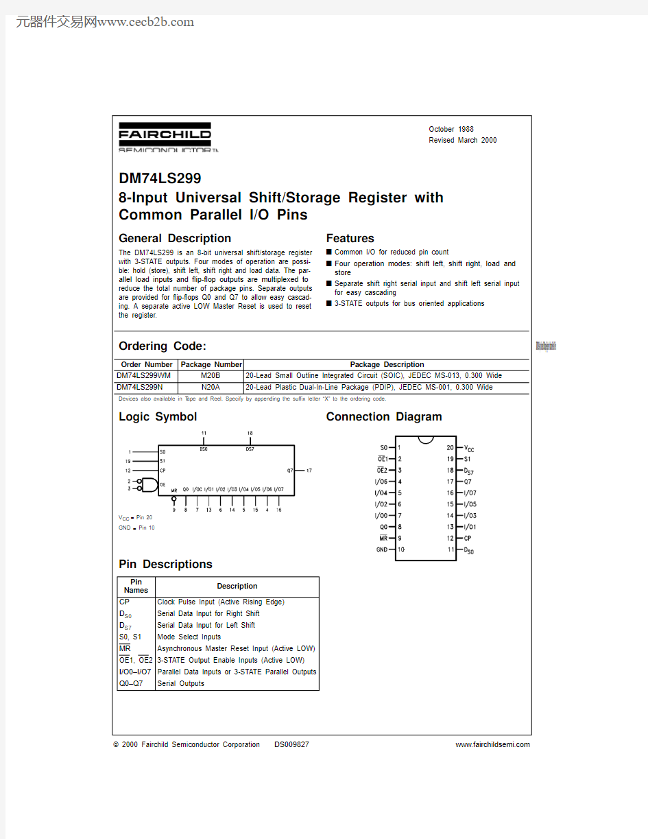
Logic Symbol V CC = Pin 20GND = Pin 10
Pin Descriptions
Connection Diagram
Order Number Package Number
Package Description
DM74LS299WM M20B 20-Lead Small Outline Integrated Circuit (SOIC), JEDEC MS-013, 0.300 Wide DM74LS299N
N20A
20-Lead Plastic Dual-In-Line Package (PDIP), JEDEC MS-001, 0.300 Wide
Pin Names Description
CP Clock Pulse Input (Active Rising Edge)D S0Serial Data Input for Right Shift D S7Serial Data Input for Left Shift S0, S1Mode Select Inputs
MR
Asynchronous Master Reset Input (Active LOW)
OE1, OE23-STATE Output Enable Inputs (Active LOW)I/O0–I/O7Parallel Data Inputs or 3-STATE Parallel Outputs Q0–Q7
Serial Outputs
https://www.doczj.com/doc/1f15548216.html, 2
D M 74L S 299
Functional Description
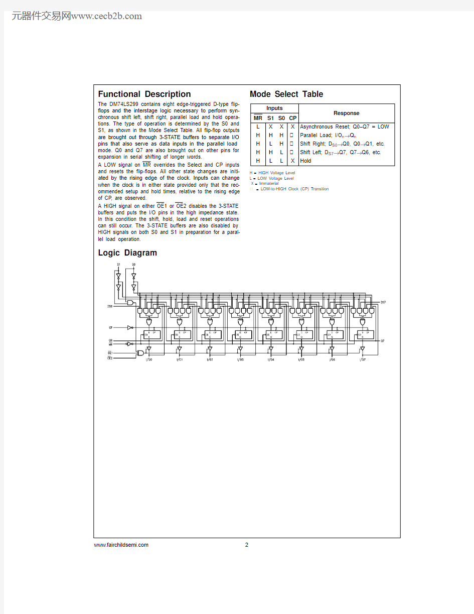
The DM74LS299 contains eight edge-triggered D-type flip-flops and the interstage logic necessary to perform syn-chronous shift left, shift right, parallel load and hold opera-tions. The type of operation is determined by the S0 and S1, as shown in the Mode Select Table. All flip-flop outputs are brought out through 3-STATE buffers to separate I/O pins that also serve as data inputs in the parallel load mode. Q0 and Q7 are also brought out on other pins for expansion in serial shifting of longer words.
A LOW signal on MR overrides the Select and CP inputs and resets the flip-flops. All other state changes are initi-ated by the rising edge of the clock. Inputs can change when the clock is in either state provided only that the rec-ommended setup and hold times, relative to the rising edge of CP, are observed.
A HIGH signal on either OE1 or OE2 disables the 3-STATE buffers and puts the I/O pins in the high impedance state.In this condition the shift, hold, load and reset operations can still occur. The 3-STATE buffers are also disabled by HIGH signals on both S0 and S1 in preparation for a paral-lel load operation.
Mode Select Table
H = HIGH Voltage Level L = LOW Voltage Level X = Immaterial
= LOW-to-HIGH Clock (CP) Transition
Logic Diagram
Inputs Response
MR S1S0CP L X X X
Asynchronous Reset; Q0–Q7 = LOW
H H H Parallel Load; I/O n →Q n
H L H Shift Right; D S0→Q0, Q0→Q1, etc.H H L Shift Left; D S7→Q7, Q7→Q6, etc.H
L
L
X
Hold
https://www.doczj.com/doc/1f15548216.html,
DM74LS299
Absolute Maximum Ratings (Note 1)
Note 1: The “Absolute Maximum Ratings” are those values beyond which the safety of the device cannot be guaranteed. The device should not be operated at these limits. The parametric values defined in the Electrical Characteristics tables are not guaranteed at the absolute maximum ratings.The “Recommended Operating Conditions” table will define the conditions for actual device operation.
Recommended Operating Conditions
Supply Voltage 7V Input Voltage
7V
Operating Free Air Temperature Range 0°C to +70°C Storage Temperature Range
?65°C to +150°C
Symbol Parameter
Min Nom Max Units V CC Supply Voltage
4.755
5.25
V V IH HIGH Level Input Voltage 2
V V IL LOW Level Input Voltage 0.8V I OH HIGH Level Output Current Q0, Q7?0.4mA I/O0–I/O7?2.6mA I OL LOW Level Output Current Q0, Q78mA I/O0–I/O7
24mA T A Free Air Operating Temperature 070
°C t S (H)Setup Time HIGH or LOW 24ns t S (L)S0 or S1 to CP
24t H (H)Hold Time HIGH or LOW 0ns t H (L)S0 or S1 to CP
0t S (H)Setup Time HIGH or LOW 10ns t S (L)I/O n , D S0, D S7 to CP 10t H (H)Hold Time HIGH or LOW 0ns t H (L)I/O n , D S0, D S7 to CP
0t W (H)CP Pulse Width HIGH or LOW
15ns t W (L)15t W (L)MR Pulse Width LOW 15ns t REC
Recovery Time 10
ns
MR to CP
https://www.doczj.com/doc/1f15548216.html, 4
D M 74L S 299
Electrical Characteristics
Over recommended operating free air temperature range (unless otherwise noted)Note 2: All typicals are at V CC = 5V, T A = 25°C.
Note 3: Not more than one output should be shorted at a time, and the duration should not exceed one second.
Switching Characteristics
V CC = +5.0V, T A = +25°C
Symbol Parameter
Conditions
Min
Typ Max Units (Note 2)V I Input Clamp Voltage V CC = Min, I I = ?18 mA ?1.5
V V OH HIGH Level V CC = Min, I OH = Max Q0, Q7 2.7 3.4
V
Output Voltage V IL = Max I/O0–I/O7
2.4
V OL
LOW Level V CC = Min, I OL = Max
0.350.5Output Voltage
V IH = Min
V I OL = 4 mA, V CC = Min 0.25
0.4I I Input Current @ Max V CC = Max Inputs 0.1mA Input Voltage V I = 7V
Sn 0.2mA I IH HIGH Level V CC = Max, V I = 2.7V
Sn 40μA Input Current
Inputs 20μA I IL LOW Level V CC = Max, V I = 0.4V Sn ?0.8mA Input Current Inputs
?0.4
mA I OS Short Circuit V CC = Max Q 0, Q 7?20?100mA Output Current (Note 3)
I/O 0–I/O 7
?30
?130I CC Supply Current V CC = Max, OE = 4.5V 60mA I OZH 3-STATE Output Off V CC = Max 40μA Current HIGH V O = 2.7V I OZL
3-STATE Output Off V CC = Max ?400
μA
Current Low
V O = 0.4V
Symbol Parameter
R L = 2 k ?
Units
C L = 15 pF
Min
Max
f MAX Maximum Input Frequency 35
MHz t PLH Propagation Delay 26ns t PHL CP to Q0 or Q728t PLH Propagation Delay 25ns t PHL CP to I/O n
35t PHL Propagation Delay 28ns MR to Q0 or Q7t PHL Propagation Delay 35ns MR to I/O n
t PZH Output Enable Time
18ns t PZL 25t PHZ Output Disable Time
15ns t PLZ
20
https://www.doczj.com/doc/1f15548216.html,
DM74LS299
Physical Dimensions inches (millimeters) unless otherwise noted
20-Lead Small Outline Integrated Circuit (SOIC), JEDEC MS-013, 0.300 Wide
Package Number M20B
https://www.doczj.com/doc/1f15548216.html,
6
D M 74L S 299 8-I n p u t U n i v e r s a l S h i f t /S t o r a g e R e g i s t e r w i t h C o m m o n P a r a l l e l I /O P i n s
Physical Dimensions inches (millimeters) unless otherwise noted (Continued)
20-Lead Plastic Dual-In-Line Package (PDIP), JEDEC MS-001, 0.300 Wide
Package Number N20A
Fairchild does not assume any responsibility for use of any circuitry described, no circuit patent licenses are implied and Fairchild reserves the right at any time without notice to change said circuitry and specifications.LIFE SUPPORT POLICY
FAIRCHILD’S PRODUCTS ARE NOT AUTHORIZED FOR USE AS CRITICAL COMPONENTS IN LIFE SUPPORT DEVICES OR SYSTEMS WITHOUT THE EXPRESS WRITTEN APPROVAL OF THE PRESIDENT OF FAIRCHILD SEMICONDUCTOR CORPORATION. As used herein:1.Life support devices or systems are devices or systems which, (a) are intended for surgical implant into the body, or (b) support or sustain life, and (c) whose failure to perform when properly used in accordance with instructions for use provided in the labeling, can be rea-sonably expected to result in a significant injury to the user. 2. A critical component in any component of a life support device or system whose failure to perform can be rea-sonably expected to cause the failure of the life support device or system, or to affect its safety or effectiveness.
https://www.doczj.com/doc/1f15548216.html,