Design of NDIR gas sensor with two F-P absorber-structures working as IR-emitter and IR-detector
- 格式:pdf
- 大小:3.98 MB
- 文档页数:8
(二 0 一 二 年 六 月本科毕业设计说明书 学校代码: 10128 学 号:************题 目:家用燃气泄漏报警装置的设计 学生姓名: 学 院:机械学院 系 别:测控系 专 业:测控技术与仪器 班 级:测控08-1 指导教师: 高 级 实 验 师摘要燃气(人工煤气、天然气)的普及,为市民提供了方便,也提高市民的生活质量,但是任何事物都有它的两面性,在使用燃气的过程中,因燃气泄漏等原因造成的燃气爆炸、中毒等意外事故时有发生,给人们的生命和财产安全带来了严重的威胁,因此安全使用燃气,是不可忽视的一个重中之重的工作。
家用燃气泄漏报警装置能有效监测环境中可燃气体(如CH4)的浓度,一旦其浓度超出报警限定值,就能发出声光报警信号,并且能随着浓度的增加报警音量逐渐加大,能及时起到安全防范的作用。
本设计所研究的可燃性气体报警系统包括:气体信号采集电路、调理电路、模数转化电路、单片机系统电路、报警电路组成,首先利用传感器对可燃气体浓度信号进行监测并且转变成电压信号,选择合适的放大电路,将电压放大到A/D 所要求的电压,经过模数转换,将检测的电压值送入单片机,在单片机内完成与设定的电压信号进行比较,当气体浓度超标时,驱动声音和灯光报警。
关键词:传感器;报警器;单片机AbstractWith the popularity of Gas ,for example( artificial coal gas, natural gas ), It is provide a convenient to citizens and improve the quality of lives, But every coin has its two sides,at the use of gas in the process, gas explosion caused by gas leak, So that poisoning and other accidents have occurred, It is harm for people and property and brings the seriously threat to the safe use of gas at the same time, The Domestic gas leakage alarm device can effectively monitor the environment of combustible gases (such as CH4) leakage, Once its concentration beyond the alarm limit value, can send out sound and light alarm signals, and with the increasing concentration of alarm volume increased gradually, The alarm plays a significant role. the sensor especially gas sensors usage and use research are needed.The design and research of the family gas alarm system includes: gas signal acquisition circuit, analog-to-digital conversion electric control circuit, The signals are monitored and converted into voltage signal, select the appropriate amplification circuit, the voltage amplification to the requirement of the A/D voltage, after analog-digital conversion, the detected voltage value into the microcontroller, in the MCU completed within the voltage signal is compared with the set, when the gas concentration exceed the standard, drive the sound and light alarm.Keywords: sensor;alarm;SCM目录引言 (1)第一章概述 (2)1.1家用燃气泄露报警的概述 (2)1.2家用燃气泄露报警的发展 (2)1.3家用燃气泄露报警研究的目的与意义 (3)第二章燃气检测传感器的选择 (4)2.1气体传感器的选型 (4)2.1.1气体传感器介绍 (4)2.2.2气体传感器的主要参数和特性 (7)2.2.2气体传感器的选定 (8)2.2.3 MC101介绍 (8)第三章家用燃气泄露报警装置的硬件部分设计 (11)3.1系统硬件电路总体设计 (11)3.2家用燃气报警器的功能 (11)3.2.1声光报警功能 (11)3.2.2标准工作条件 (11)3.2.3外围接口电路的设计 (16)3.2.4 A/D转换主要技术指标 (18)3.2.5单片机与ADC0808接口电路 (18)3.2.6串口转并口芯片74HC164 (19)3.2.7数码管显示 (20)3.2.8声音灯光报警电路 (22)3.3总电路设计 (22)第四章燃气泄漏报警系统的软件部分设计 (24)4.1软件设计重要性 (24)4.2主程序设计流程图 (24)4.3软件设计的子程序基本思想 (28)4.3.1A/D转换 (28)4.3.2浓度转换 (29)4.3.3 数码显示 (30)结论 (32)谢辞 (33)参考文献 (34)图表清单表2-1 各种气体传感器可检测的气体种类 (7)表2-2 MC101技术指标 (8)图2-1 灵敏度特性图 (9)图2-2响应恢复特性图 (9)图2-3 输出信号随环境温度的变化图 (9)图2-4 输出信号随环境温度的变化图 (10)图2-5 输出信号随工作电压的变化图 (10)图2-6 输出信号随工作电压的变化图 (10)图2-7 传感器基本测试电路图 (10)表3-1 地址选通输入端 (17)表3-2引脚说明 (20)表3-3功能表 (20)图3-1燃气报警系统结构框图 (12)图3-2 AT89C51单片机 (12)图3-3时钟和复位电路 (15)图3-4电源电路电路、信号采集及放大电路 (16)图3-5 ADC0808引脚图 (17)图3-6单片机与0808接口电路 (19)图3-7 74HC164 (19)图3-8数码管显示图 (21)图3-9 声音灯光报警电路 (22)图3-10燃气报警系统总电路图 (23)图4-1 主程序流程图 (28)图4-2 A/D转换程序流程图 (28)图4-3 浓度转换流程图 (29)图4-4数码管显示流程图 (30)引言随着我国燃气的变革及西气东输工程的进行,目前家家户户做饭离不开煤气、天然气,一旦泄露后果不堪设想,每年,因煤气泄漏引发的中毒事件,或因室内燃气泄漏浓度过高引起的爆炸,类似的事件也不少见。

NDIR红外气体传感器的基本概述NDIR红外气体传感器(Non-dispersive Infrared Gas Sensor)是一种利用红外辐射原理检测气体浓度的传感器。
它由红外光源、气体室、红外滤波器、检测器以及电子信号处理电路等组成。
这种传感器主要用于测量空气中的气体浓度,如CO2、CO、CH4等。
NDIR传感器的工作原理是通过红外吸收特性来检测气体浓度。
当红外光源照射到气体室中的气体时,气体中的特定组分会吸收特定波长的红外光,吸收光的强度与气体浓度成正比。
检测器接收红外光,并通过与光源的参考信号进行比较,计算出气体的浓度值。
为了提高传感器的性能,NDIR传感器通常使用窄带滤波器,以选择性地传递特定波长的红外光。
这样可以排除其他波长的干扰光,提高气体浓度的测量精度。
NDIR传感器有许多优点。
首先,它具有高度可选择性。
通过选择不同的滤波器,可以检测多种气体,从而适应不同的应用需求。
其次,NDIR传感器灵敏度高,可检测到极低浓度的气体。
同时,它对温度和湿度的依赖性也较小,可以在不同的环境条件下进行可靠的气体浓度测量。
此外,NDIR传感器具有快速响应时间和长寿命的特点。
然而,NDIR传感器也存在一些局限性。
首先,由于传感器本身的设计和结构复杂,其制造成本较高。
另外,一些特定的气体分子如氧气(O2)和水蒸气(H2O)具有较高的红外吸收能力,这可能会导致测量上的干扰。
此外,NDIR传感器的响应时间较慢,无法实现实时监测。
为了克服这些问题,研究者们正在不断改进NDIR传感器的设计和技术。
他们提出了多通道测量、温湿度补偿和智能算法等方法来提高传感器的性能。
此外,一些新型材料的应用也为NDIR传感器的发展提供了新的可能性。
总之,NDIR红外气体传感器是一种重要的气体浓度检测工具。
它通过利用红外光的吸收特性来测量气体浓度,具有高度可选择性、高灵敏度和稳定性等优点。
随着技术的发展,NDIR传感器在环境监测、工业安全和室内空气质量监测等领域的应用将会越来越广泛。
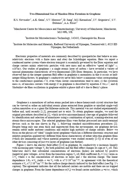
Two-Dimensional Gas of Massless Dirac Fermions in Graphene K.S. Novoselov1, A.K. Geim1, S.V. Morozov2, D. Jiang1, M.I. Katsnelson3, I.V. Grigorieva1, S.V. Dubonos2, A.A. Firsov21Manchester Centre for Mesoscience and Nanotechnology, University of Manchester, Manchester, M13 9PL, UK2Institute for Microelectronics Technology, 142432, Chernogolovka, Russia3Institute for Molecules and Materials, Radboud University of Nijmegen, Toernooiveld 1, 6525 ED Nijmegen, the NetherlandsElectronic properties of materials are commonly described by quasiparticles that behave as nonrelativistic electrons with a finite mass and obey the Schrödinger equation. Here we report a condensed matter system where electron transport is essentially governed by the Dirac equation and charge carriers mimic relativistic particles with zero mass and an effective “speed of light” c∗ ≈106m/s. Our studies of graphene – a single atomic layer of carbon – have revealed a variety of unusual phenomena characteristic of two-dimensional (2D) Dirac fermions. In particular, we have observed that a) the integer quantum Hall effect in graphene is anomalous in that it occurs at halfinteger filling factors; b) graphene’s conductivity never falls below a minimum value corresponding to the conductance quantum e2/h, even when carrier concentrations tend to zero; c) the cyclotron mass mc of massless carriers with energy E in graphene is described by equation E =mcc∗2; and d) Shubnikov-de Haas oscillations in graphene exhibit a phase shift of π due to Berry’s phase.Graphene is a monolayer of carbon atoms packed into a dense honeycomb crystal structure that can be viewed as either an individual atomic plane extracted from graphite or unrolled single-wall carbon nanotubes or as a giant flat fullerene molecule. This material was not studied experimentally before and, until recently [1,2], presumed not to exist. To obtain graphene samples, we used the original procedures described in [1], which involve micromechanical cleavage of graphite followed by identification and selection of monolayers using a combination of optical, scanning-electron and atomic-force microscopies. The selected graphene films were further processed into multi-terminal devices such as the one shown in Fig. 1, following standard microfabrication procedures [2]. Despite being only one atom thick and unprotected from the environment, our graphene devices remain stable under ambient conditions and exhibit high mobility of charge carriers. Below we focus on the physics of “ideal” (single-layer) graphene which has a different electronic structure and exhibits properties qualitatively different from those characteristic of either ultra-thin graphite films (which are semimetals and whose material properties were studied recently [2-5]) or even of our other devices consisting of just two layers of graphene (see further). Figure 1 shows the electric field effect [2-4] in graphene. Its conductivity σ increases linearly with increasing gate voltage Vg for both polarities and the Hall effect changes its sign at Vg ≈0. This behaviour shows that substantial concentrations of electrons (holes) are induced by positive (negative) gate voltages. Away from the transition region Vg ≈0, Hall coefficient RH = 1/ne varies as 1/Vg where n is the concentration of electrons or holes and e the electron charge. The linear dependence 1/RH ∝Vg yields n =α·Vg with α ≈7.3·1010cm-2/V, in agreement with the theoretical estimate n/Vg ≈7.2·1010cm-2/V for the surface charge density induced by the field effect (see Fig. 1’s caption). The agreement indicates that all the induced carriers are mobile and there are no trapped charges in graphene. From the linear dependence σ(Vg) we found carrier mobilities µ =σ/ne, whichreached up to 5,000 cm2/Vs for both electrons and holes, were independent of temperature T between 10 and 100K and probably still limited by defects in parent graphite. To characterise graphene further, we studied Shubnikov-de Haas oscillations (SdHO). Figure 2 shows examples of these oscillations for different magnetic fields B, gate voltages and temperatures. Unlike ultra-thin graphite [2], graphene exhibits only one set of SdHO for both electrons and holes. By using standard fan diagrams [2,3], we have determined the fundamental SdHO frequency BF for various Vg. The resulting dependence of BF as a function of n is plotted in Fig. 3a. Both carriers exhibit the same linear dependence BF = β·n with β ≈1.04·10-15 T·m2 (±2%). Theoretically, for any 2D system β is defined only by its degeneracy f so that BF =φ0n/f, where φ0 =4.14·10-15 T·m2 is the flux quantum. Comparison with the experiment yields f =4, in agreement with the double-spin and double-valley degeneracy expected for graphene [6,7] (cf. caption of Fig. 2). Note however an anomalous feature of SdHO in graphene, which is their phase. In contrast to conventional metals, graphene’s longitudinal resistance ρxx(B) exhibits maxima rather than minima at integer values of the Landau filling factor ν (Fig. 2a). Fig. 3b emphasizes this fact by comparing the phase of SdHO in graphene with that in a thin graphite film [2]. The origin of the “odd” phase is explained below. Another unusual feature of 2D transport in graphene clearly reveals itself in the T-dependence of SdHO (Fig. 2b). Indeed, with increasing T the oscillations at high Vg (high n) decay more rapidly. One can see that the last oscillation (Vg ≈100V) becomes practically invisible already at 80K whereas the first one (Vg <10V) clearly survives at 140K and, in fact, remains notable even at room temperature. To quantify this behaviour we measured the T-dependence of SdHO’s amplitude at various gate voltages and magnetic fields. The results could be fitted accurately (Fig. 3c) by the standard expression T/sinh(2π2kBTmc/heB), which yielded mc varying between ≈ 0.02 and 0.07m0 (m0 is the free electron mass). Changes in mc are well described by a square-root dependence mc ∝n1/2 (Fig. 3d). To explain the observed behaviour of mc, we refer to the semiclassical expressions BF = (h/2πe)S(E) and mc =(h2/2π)∂S(E)/∂E where S(E) =πk2 is the area in k-space of the orbits at the Fermi energy E(k) [8]. Combining these expressions with the experimentally-found dependences mc ∝n1/2 and BF =(h/4e)n it is straightforward to show that S must be proportional to E2 which yields E ∝k. Hence, the data in Fig. 3 unambiguously prove the linear dispersion E =hkc∗ for both electrons and holes with a common origin at E =0 [6,7]. Furthermore, the above equations also imply mc =E/c∗2 =(h2n/4πc∗2)1/2 and the best fit to our data yields c∗ ≈1⋅106 m/s, in agreement with band structure calculations [6,7]. The employed semiclassical model is fully justified by a recent theory for graphene [9], which shows that SdHO’s amplitude can indeed be described by the above expression T/sinh(2π2kBTmc/heB) with mc =E/c∗2. Note that, even though the linear spectrum of fermions in graphene (Fig. 3e) implies zero rest mass, their cyclotron mass is not zero. The unusual response of massless fermions to magnetic field is highlighted further by their behaviour in the high-field limit where SdHO evolve into the quantum Hall effect (QHE). Figure 4 shows Hall conductivity σxy of graphene plotted as a function of electron and hole concentrations in a constant field B. Pronounced QHE plateaux are clearly seen but, surprisingly, they do not occur in the expected sequence σxy =(4e2/h)N where N is integer. On the contrary, the plateaux correspond to half-integer ν so that the first plateau occurs at 2e2/h and the sequence is (4e2/h)(N + ½). Note that the transition from the lowest hole (ν =–½) to lowest electron (ν =+½) Landau level (LL) in graphene requires the same number of carriers (∆n =4B/φ0 ≈1.2·1012cm-2) as the transition between other nearest levels (cf. distances between minima in ρxx). This results in a ladder of equidistant steps in σxy which are not interrupted when passing through zero. To emphasize this highly unusual behaviour, Fig. 4 also shows σxy for a graphite film consisting of only two graphene layers where the sequence of plateaux returns to normal and the first plateau is at 4e2/h, as in the conventional QHE. We attribute this qualitative transition between graphene and its two-layer counterpart to the fact that fermions in the latter exhibit a finite mass near n ≈0 (as found experimentally; to be published elsewhere) and can no longer be described as massless Dirac particles. 2The half-integer QHE in graphene has recently been suggested by two theory groups [10,11], stimulated by our work on thin graphite films [2] but unaware of the present experiment. The effect is single-particle and intimately related to subtle properties of massless Dirac fermions, in particular, to the existence of both electron- and hole-like Landau states at exactly zero energy [912]. The latter can be viewed as a direct consequence of the Atiyah-Singer index theorem that plays an important role in quantum field theory and the theory of superstrings [13,14]. For the case of 2D massless Dirac fermions, the theorem guarantees the existence of Landau states at E=0 by relating the difference in the number of such states with opposite chiralities to the total flux through the system (note that magnetic field can also be inhomogeneous). To explain the half-integer QHE qualitatively, we invoke the formal expression [9-12] for the energy of massless relativistic fermions in quantized fields, EN =[2ehc∗2B(N +½ ±½)]1/2. In QED, sign ± describes two spins whereas in the case of graphene it refers to “pseudospins”. The latter have nothing to do with the real spin but are “built in” the Dirac-like spectrum of graphene, and their origin can be traced to the presence of two carbon sublattices. The above formula shows that the lowest LL (N =0) appears at E =0 (in agreement with the index theorem) and accommodates fermions with only one (minus) projection of the pseudospin. All other levels N ≥1 are occupied by fermions with both (±) pseudospins. This implies that for N =0 the degeneracy is half of that for any other N. Alternatively, one can say that all LL have the same “compound” degeneracy but zeroenergy LL is shared equally by electrons and holes. As a result the first Hall plateau occurs at half the normal filling and, oddly, both ν = –½ and +½ correspond to the same LL (N =0). All other levels have normal degeneracy 4B/φ0 and, therefore, remain shifted by the same ½ from the standard sequence. This explains the QHE at ν =N + ½ and, at the same time, the “odd” phase of SdHO (minima in ρxx correspond to plateaux in ρxy and, hence, occur at half-integer ν; see Figs. 2&3), in agreement with theory [9-12]. Note however that from another perspective the phase shift can be viewed as the direct manifestation of Berry’s phase acquired by Dirac fermions moving in magnetic field [15,16]. Finally, we return to zero-field behaviour and discuss another feature related to graphene’s relativistic-like spectrum. The spectrum implies vanishing concentrations of both carriers near the Dirac point E =0 (Fig. 3e), which suggests that low-T resistivity of the zero-gap semiconductor should diverge at Vg ≈0. However, neither of our devices showed such behaviour. On the contrary, in the transition region between holes and electrons graphene’s conductivity never falls below a well-defined value, practically independent of T between 4 and 100K. Fig. 1c plots values of the maximum resistivity ρmax(B =0) found in 15 different devices, which within an experimental error of ≈15% all exhibit ρmax ≈6.5kΩ, independent of their mobility that varies by a factor of 10. Given the quadruple degeneracy f, it is obvious to associate ρmax with h/fe2 =6.45kΩ where h/e2 is the resistance quantum. We emphasize that it is the resistivity (or conductivity) rather than resistance (or conductance), which is quantized in graphene (i.e., resistance R measured experimentally was not quantized but scaled in the usual manner as R =ρL/w with changing length L and width w of our devices). Thus, the effect is completely different from the conductance quantization observed previously in quantum transport experiments. However surprising, the minimum conductivity is an intrinsic property of electronic systems described by the Dirac equation [17-20]. It is due to the fact that, in the presence of disorder, localization effects in such systems are strongly suppressed and emerge only at exponentially large length scales. Assuming the absence of localization, the observed minimum conductivity can be explained qualitatively by invoking Mott’s argument [21] that mean-free-path l of charge carriers in a metal can never be shorter that their wavelength λF. Then, σ =neµ can be re-written as σ = (e2/h)kFl and, hence, σ cannot be smaller than ≈e2/h per each type of carriers. This argument is known to have failed for 2D systems with a parabolic spectrum where disorder leads to localization and eventually to insulating behaviour [17,18]. For the case of 2D Dirac fermions, no localization is expected [17-20] and, accordingly, Mott’s argument can be used. Although there is a broad theoretical consensus [18-23,10,11] that a 2D gas of Dirac fermions should exhibit a minimum 3conductivity of about e2/h, this quantization was not expected to be accurate and most theories suggest a value of ≈e2/πh, in disagreement with the experiment. In conclusion, graphene exhibits electronic properties distinctive for a 2D gas of particles described by the Dirac rather than Schrödinger equation. This 2D system is not only interesting in itself but also allows one to access – in a condensed matter experiment – the subtle and rich physics of quantum electrodynamics [24-27] and provides a bench-top setting for studies of phenomena relevant to cosmology and astrophysics [27,28].1. Novoselov, K.S. et al. PNAS 102, 10451 (2005). 2. Novoselov, K.S. et al. Science 306, 666 (2004); cond-mat/0505319. 3. Zhang, Y., Small, J.P., Amori, M.E.S. & Kim, P. Phys. Rev. Lett. 94, 176803 (2005). 4. Berger, C. et al. J. Phys. Chem. B, 108, 19912 (2004). 5. Bunch, J.S., Yaish, Y., Brink, M., Bolotin, K. & McEuen, P.L. Nanoletters 5, 287 (2005). 6. Dresselhaus, M.S. & Dresselhaus, G. Adv. Phys. 51, 1 (2002). 7. Brandt, N.B., Chudinov, S.M. & Ponomarev, Y.G. Semimetals 1: Graphite and Its Compounds (North-Holland, Amsterdam, 1988). 8. Vonsovsky, S.V. and Katsnelson, M.I. Quantum Solid State Physics (Springer, New York, 1989). 9. Gusynin, V.P. & Sharapov, S.G. Phys. Rev. B 71, 125124 (2005). 10. Gusynin, V.P. & Sharapov, S.G. cond-mat/0506575. 11. Peres, N.M.R., Guinea, F. & Castro Neto, A.H. cond-mat/0506709. 12. Zheng, Y. & Ando, T. Phys. Rev. B 65, 245420 (2002). 13. Kaku, M. Introduction to Superstrings (Springer, New York, 1988). 14. Nakahara, M. Geometry, Topology and Physics (IOP Publishing, Bristol, 1990). 15. Mikitik, G. P. & Sharlai, Yu.V. Phys. Rev. Lett. 82, 2147 (1999). 16. Luk’yanchuk, I.A. & Kopelevich, Y. Phys. Rev. Lett. 93, 166402 (2004). 17. Abrahams, E., Anderson, P.W., Licciardello, D.C. & Ramakrishnan, T.V. Phys. Rev. Lett. 42, 673 (1979). 18. Fradkin, E. Phys. Rev. B 33, 3263 (1986). 19. Lee, P.A. Phys. Rev. Lett. 71, 1887 (1993). 20. Ziegler, K. Phys. Rev. Lett. 80, 3113 (1998). 21. Mott, N.F. & Davis, E.A. Electron Processes in Non-Crystalline Materials (Clarendon Press, Oxford, 1979). 22. Morita, Y. & Hatsugai, Y. Phys. Rev. Lett. 79, 3728 (1997). 23. Nersesyan, A.A., Tsvelik, A.M. & Wenger, F. Phys. Rev. Lett. 72, 2628 (1997). 24. Rose, M.E. Relativistic Electron Theory (John Wiley, New York, 1961). 25. Berestetskii, V.B., Lifshitz, E.M. & Pitaevskii, L.P. Relativistic Quantum Theory (Pergamon Press, Oxford, 1971). 26. Lai, D. Rev. Mod. Phys. 73, 629 (2001). 27. Fradkin, E. Field Theories of Condensed Matter Systems (Westview Press, Oxford, 1997). 28. Volovik, G.E. The Universe in a Helium Droplet (Clarendon Press, Oxford, 2003).Acknowledgements This research was supported by the EPSRC (UK). We are most grateful to L. Glazman, V. Falko, S. Sharapov and A. Castro Netto for helpful discussions. K.S.N. was supported by Leverhulme Trust. S.V.M., S.V.D. and A.A.F. acknowledge support from the Russian Academy of Science and INTAS.43µ (m2/Vs)0.8c4P0.4 22 σ (1/kΩ)10K0 0 1/RH(T/kΩ) 1 2ρmax (h/4e2)1-5010 Vg (V) 50 -10ab 0 -100-500 Vg (V)50100Figure 1. Electric field effect in graphene. a, Scanning electron microscope image of one of our experimental devices (width of the central wire is 0.2µm). False colours are chosen to match real colours as seen in an optical microscope for larger areas of the same materials. Changes in graphene’s conductivity σ (main panel) and Hall coefficient RH (b) as a function of gate voltage Vg. σ and RH were measured in magnetic fields B =0 and 2T, respectively. The induced carrier concentrations n are described by [2] n/Vg =ε0ε/te where ε0 and ε are permittivities of free space and SiO2, respectively, and t ≈300 nm is the thickness of SiO2 on top of the Si wafer used as a substrate. RH = 1/ne is inverted to emphasize the linear dependence n ∝Vg. 1/RH diverges at small n because the Hall effect changes its sign around Vg =0 indicating a transition between electrons and holes. Note that the transition region (RH ≈ 0) was often shifted from zero Vg due to chemical doping [2] but annealing of our devices in vacuum normally allowed us to eliminate the shift. The extrapolation of the linear slopes σ(Vg) for electrons and holes results in their intersection at a value of σ indistinguishable from zero. c, Maximum values of resistivity ρ =1/σ (circles) exhibited by devices with different mobilites µ (left y-axis). The histogram (orange background) shows the number P of devices exhibiting ρmax within 10% intervals around the average value of ≈h/4e2. Several of the devices shown were made from 2 or 3 layers of graphene indicating that the quantized minimum conductivity is a robust effect and does not require “ideal” graphene.ρxx (kΩ)0.60 aVg = -60V4B (T)810K12∆σxx (1/kΩ)0.4 1ν=4 140K 80K B =12T0 b 0 25 50 Vg (V) 7520K100Figure 2. Quantum oscillations in graphene. SdHO at constant gate voltage Vg as a function of magnetic field B (a) and at constant B as a function of Vg (b). Because µ does not change much with Vg, the constant-B measurements (at a constant ωcτ =µB) were found more informative. Panel b illustrates that SdHO in graphene are more sensitive to T at high carrier concentrations. The ∆σxx-curves were obtained by subtracting a smooth (nearly linear) increase in σ with increasing Vg and are shifted for clarity. SdHO periodicity ∆Vg in a constant B is determined by the density of states at each Landau level (α∆Vg = fB/φ0) which for the observed periodicity of ≈15.8V at B =12T yields a quadruple degeneracy. Arrows in a indicate integer ν (e.g., ν =4 corresponds to 10.9T) as found from SdHO frequency BF ≈43.5T. Note the absence of any significant contribution of universal conductance fluctuations (see also Fig. 1) and weak localization magnetoresistance, which are normally intrinsic for 2D materials with so high resistivity.75 BF (T) 500.2 0.11/B (1/T)b5 10 N 1/2025 a 0 0.061dmc /m00.04∆0.02 0c0 0 T (K) 150n =0e-6-3036Figure 3. Dirac fermions of graphene. a, Dependence of BF on carrier concentration n (positive n correspond to electrons; negative to holes). b, Examples of fan diagrams used in our analysis [2] to find BF. N is the number associated with different minima of oscillations. Lower and upper curves are for graphene (sample of Fig. 2a) and a 5-nm-thick film of graphite with a similar value of BF, respectively. Note that the curves extrapolate to different origins; namely, to N = ½ and 0. In graphene, curves for all n extrapolate to N = ½ (cf. [2]). This indicates a phase shift of π with respect to the conventional Landau quantization in metals. The shift is due to Berry’s phase [9,15]. c, Examples of the behaviour of SdHO amplitude ∆ (symbols) as a function of T for mc ≈0.069 and 0.023m0; solid curves are best fits. d, Cyclotron mass mc of electrons and holes as a function of their concentration. Symbols are experimental data, solid curves the best fit to theory. e, Electronic spectrum of graphene, as inferred experimentally and in agreement with theory. This is the spectrum of a zero-gap 2D semiconductor that describes massless Dirac fermions with c∗ 300 times less than the speed of light.n (1012 cm-2)σxy (4e2/h)4 3 2 -2 1 -1 -2 -3 2 44Kn7/ 5/ 3/ 1/2 2 2 210 ρxx (kΩ)-4σxy (4e2/h)0-1/2 -3/2 -5/2514T0-7/2 -4 -2 0 2 4 n (1012 cm-2)Figure 4. Quantum Hall effect for massless Dirac fermions. Hall conductivity σxy and longitudinal resistivity ρxx of graphene as a function of their concentration at B =14T. σxy =(4e2/h)ν is calculated from the measured dependences of ρxy(Vg) and ρxx(Vg) as σxy = ρxy/(ρxy + ρxx)2. The behaviour of 1/ρxy is similar but exhibits a discontinuity at Vg ≈0, which is avoided by plotting σxy. Inset: σxy in “two-layer graphene” where the quantization sequence is normal and occurs at integer ν. The latter shows that the half-integer QHE is exclusive to “ideal” graphene.。

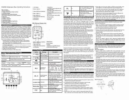
Intelligent Infrared CO2 Gas Sensor(Model: MH-711A)ManualVersion: 3.3Valid from: May 1st, 2014 Zhengzhou Winsen Electronics Technology Co., Ltd.StatementThis manual copyright belongs to Zhengzhou Winsen Electronics Technology Co., LTD. Without the written permission, any part of this manual shall not be copied, translated, stored in database or retrieval system, also can’t spread through electronic, copying, record ways.Thanks for purchasing our product. In order to keep customers using it better and reduce the faults caused by misuse, please read the manual carefully and operate it correctly in accordance with the instructions. If users disobey the terms or remove, disassemble, change the components inside of the sensor, we shall not be responsible for the loss.The specific such as color, appearance, sizes etc., please in kind prevail.We are devoting ourselves to products development and technical innovation, so we reserve the right to improve the products without notice. Please confirm it is the valid version before using this manual. At the same time, users’ comments on optimized using way are welcome.Please keep the manual properly, in order to get help if you have questions during the usage in the future.Zhengzhou Winsen Electronics Technology CO., LTD.MH-711A Infrared CO2 Gas Sensor1. Product DescriptionMH-711A is a universal type intelligent sensor to detect CO2 in air taking advantages of non-dispersive infrared (NDIR) principle. With high selectivity, no oxygen dependence, high performance and long lifespan features, MH-711A also has built-in temperature compensation feature. MH-711A is a compact andhigh-performance sensor based on infrared absorption of gas detection technology, micro-machining and sophisticated circuit design.2. CharacteristicsLong lifespanHigh Sensitivity and resolution5V constant power supply, low power consumption Output method: UART, analog voltage signal, etc. Quick response & ResumeTemperature compensation, excellent linear outputAnti-poisons, anti-vapor interferenceDetect combustible gas concentration matching with flame-proof marked detector in area 1&2explosive environments which mix of ⅡA, ⅡB, ⅡC and T1-T6 flammable gases, vapors and air3. ApplicationWidely used for industrial field instrumentation, industrial-process control and safety protection4. Technical ParametersProduct Model MH-711A Target Gas CO2 Working Voltage 4.5 V ~ 5.5V DC Average Current < 100mA Interface Level 3.3VMeasurement Range 0~30%VOL optional (view table 2)Output Signal IIC 0.4-2V DC Warm-up Time 3min Response Time T 90 < 30s Working Temp. -40℃ ~ 70℃Working Humidity0 to 95%RH, Non-condensingDimension Φ44×61mm Weight 350g Lifespan >5 years Ex-marking Ex d ⅡC T6 GbProtected ClassIP65Table 1 Technical IndexTable 2: Measurement Range and Accuracy5. Structural DrawingFigure 1 Structural Drawing of SensorFigure 2: Pin DefinitionPin DescriptionPad1 Vin (input voltage 4.5V ~5.5V) Pad4 GNDPad5 Vout (0.4~2V) Pad2 IIC(SCL) clock Pad3IIC(SDA) dataDetected GasMeasurementRange AccuracyRemarksCarbon Dioxide (CO2 gas)0~2000ppm ±50ppm +/-5% readingTemperature compensation 0~6000ppmTemperature compensation 0~1%VOL Temperature compensation 0~3%VOL Temperature compensation 0~5%VOL Temperature compensation 0~10%VOL Temperature compensation 0-30%VOL±15% reading Temperature compensationReserved, do not connectPad6, Pad7, Pad8Pad10, Pad11, Pad12Table 3: Definition of Pin6. Application CircuitFigure 3 Application CircuitExplanations:6.1: Analogue Voltage OutputVoltage output range 0.4 to 2V, relatively stands for 0 to F.S.Pad1 connect with 5V supply, Pad4 connect with VSS and Pad5 connect with input side of ADC. Then warm-up the sensor, the Vout will show a voltage value which stands for the gas concentration. If the sensor malfunctions, the output voltage is 0V.Figure 4 Analogue Voltage Output6.2 Digital OutputPad1 connect with 5V supply, Pad4 connect with VSS.Customer’s CLK connects with sensor CLK; SDA connect sensor SDA.The detector can read the value of gas concentration directly through the IIC of the sensor (The pull-up resistor of user’s SCL and SDA signal lines must be less than 10k to ensure the normal work of the communication interface), no need to calculate the gas concentration.6.2.1 Communication ProtocolMH-711A is communicated through IIC bus. The module works basing IIC slave mode and can connects to external MCU,module address: 0x55, write operation address: 0xAA, read operation address: 0xAB. Every frame number data contains 10 bytes. Different host orders lead to different data and the last byte of data is the proof test value. The SCL clock frequency is recommend less than 10K.1) Device AddressAddress format: Highest seven digits are the module add of the sensor(0x55),the least significant digit is SDIR, 0 stand for Reading, 1 stand for Writing.Table 4: Address FormatIIC communicationWrite address: 0xAA, Read address: 0xAB 2) Bus DescriptionIIC interface protocol is a special bus signal protocol, is composed of 3 parts - Start(S), Stop(P) and binary data, asshown below.At start,SCL is high,SDA is at falling edge.Aftter that,send the slave add.After the seven add digits is the control read&write digits,choose the read&write operation as above picWhen the slave device recognizes the corresponding add information,it sends a responsive signal to main device and SDA is pulled down at the ninth clock cycle.At stop,SCL keeps high level,SDA is at rising edge.Figure 5 IIC Sequence Chart3) CommandEvery frame number data of IIC communication command contains 10 bytes. Different host orders lead to different data and the last byte of data is the proof test value. Table 5 Command List0x96 Gas Concentration 0xA0 Calibrate zero point (ZERO ) 0xAACalibrate span point (SPAN )A7 A6 A5 A4 A3 A2 A1 W/R1 0 1 0 1 0 1 0/1Gas Concentration Reading1 0x96 Gas Concentration ReadingSend0 1 2 3 4 5 6 7 8 9 Command -- -- -- -- -- -- -- --CheckCode 0x96 0x00 0x00 0x00 0x00 0x00 0x00 0x00 0x00 0x6AEXP. 96 00 00 00 00 00 00 00 00 6AReturn0 1 2 3 4 5 6 7 8 9 ModuleStatusHighDensityLowDensityHighRangeLowRangeCheckCodeEXP. ReturnGas concentration= high density *256 + low density Calibrate Zero1 0xA0 Gas Concentration ReadingSend0 1 2 3 4 5 6 7 8 9 Command-- -- -- -- -- -- -- --CheckCode 0xa0 0x00 0x00 0x00 0x00 0x00 0x00 0x00 0x00 0x60EXP. A0 00 00 00 00 00 00 00 00 60Return 0 1 2 3 4 5 6 7 8 9 -- -- -- -- -- -- -- -- ---- -- -- -- -- -- -- -- --EXP. No value returnCalibrate Span1 0xAA Gas Concentration ReadingSend0 1 2 3 4 5 6 7 8 9 CommandSPAN Value -- -- -- -- -- --CheckCode 0xaaHighByteLowByte0x00 0x00 0x00 0x00 0x00 0x00 0xbbEXP. AA 13 88 00 00 00 00 00 00 BB (Eg. calibrate 5000ppm, HEX:0x1388)Return 0 1 2 3 4 5 6 7 8 9 -- -- -- -- -- -- -- -- ---- -- -- -- -- -- -- -- --EXP. No value return6.2.2 Calibrate and CalculateThe checksum = (invert (byte0 +... + 8)) + 1For example, Gas Concentration ReadingCommand SentByte0 Byte1 Byte2 Byte3 Byte4 Byte5 Byte6 Byte7 Byte8 Byte9 Command - - - - - - - - CheckValue 0x96 0x00 0x00 0x00 0x00 0x00 0x00 0x00 0x00 0x6AA. Add all the bytes together except byte 00x96 + 0 + 0 + 0 + 0 + 0 + 0 + 0 + 0 = 0x96B. Get the value from step A, then invert it.0xff – 0x96 = 0x69C. Plus one based on the value of step B0x69 + 0x01 = 0x6A6.2.3 Example ProgramC Language Calibrate & Calculate and Routinechar getCheckSum(char *packet){char i, checksum;for( i = 1; i < 9; i++){checksum += packet[i];}checksum = 0xff – checksum;checksum += 1;return checksum;}7. Notes For Maintenance7.1 The sensor should be calibrated regularly. Recommended cycle time is once per 6 months.7.2 Do not use the sensor in the high dusty environment for long time.7.3 Please use the sensor with correct power supply.Zhengzhou Winsen Electronics Technology Co., LtdAdd.: NO.299 Jinsuo Road, National Hi-Tech Zone,Zhengzhou, 450001 ChinaTel.: 0086-371-67169097Fax: 0086-371-60932988E-mail:*******************。

STABILITY CHAMBERSInstallation, Operation andMaintenance InstructionsGENERAL 2Inspection 2Location 2Installation 2DoorAlignment 2 Shelf Installation 2Contacts 2RemotePort 2RS485Outlet 2InternalPort 2AccessInstallation 3 DrainElectrical 3 Glycerin Well Assembly 3 OPERATION 4 MAINTENANCE 5Cleaning 5 PeriodicCleaning the humidifier 5-7Maintenance Service and8AnalysisGuideGENERALINSPECTIONWhen the equipment is received, all items should be carefully checked against the bill of lading to insure all crates and cartons have been received. All units should be inspected for concealed damage by uncrating the units immediately. If any damage is found, it should be reported to the carrier at once, and a claim should be filed with the carrier. This equipment has been inspected and tested in the manufacturing facility and has been crated in accordance with transportation rules and guidelines. Manufacturer is not responsible for freight loss or damage.LOCATIONThe refrigeration system located at the top of the cabinet requires free air access for proper operation. Allow a minimum four-inch clearance on the top, rear, and sides of the cabinet. The cabinet should also be leveled when it is placed in its permanent location. Do not stack items on top of the unit.Vibration during shipping and handling may loosen mechanical connections. Check all connections during installation. Check all wiring, piping and fasteners.CAUTION•Do not modify cabinet construction or associated equipment assemblies.•Do not remove labeling or information supplied with the unit.INSTALLATIONDoor Alignment - If for some reason the doors are not squared up on the cabinet, the doors can be adjusted. Opening the door(s) and loosening the screws that hold both the top and bottom hinges to the cabinet can accomplish this. After adjusting the door so that it is aligned correctly, tighten the screws to securely hold the hinges in place.Shelving Installation - Locate shelf clips in bag inside cabinet,install in shelf supports (4 per shelf)Remote contacts - Terminal board for dry contacts is locatedbehind the cabinet façade, on the left hand side of the control box,connect wires as per label.RS485 port - (Optional) terminal board for RS485 port is locatedbehind the cabinet façade, on the left hand side of the control box,connect wires as per label.Duplex/ or European Outlet - (Optional) is located near the top of the interior cabinet back. This is a15 amp 115 volt duplex PN 88010300 with its own power supply cord. Duplex outlet power cord is wrapped up on the back of the cabinet top. Outlet is not inter-wired thru main cabinet supply and must be plugged into a 115 volt/ or 220/240V power supply. Locate cabinet within 8 feet of the wall receptacle.Access Port - (Optional) is provided with a spring loaded cover on the right hand side of the cabinet.DRAIN INSTALLATIONThe Stability Chamber has a floor drain in the bottom ofthe cabinet. A silicone drain stopper has been placed inthis drain. The drain stopper will prevent undesirableliquids from running into the drain. The stopper can beremoved if any possible liquids flowing into this drain areacceptable to go to the floor drain.An 18” length of 1/2" I.D. drain hose is shipped insidecabinet. Attach hose to drain stub under cabinet withsupplied clamp and run to an atmospheric floor drain.May substitute longer drain hose as needed. Humidifierunits will require a drain for overflow.ELECTRICALFor electrical requirements see data information andwiring unit diagram located in parts bag, inside of thecabinet.Check the proposed external power outlet/supply to beused to ensure that the voltage, phase and currentcarrying capacity of the circuit from the electrical panelcorrespond to the requirements of the cabinet. NEVERuse an extension cord to wire any unit. Refer to the serialtag (nameplate data) for all pertinent electrical information.Observe all Warning Labels. Disconnect power supply(s) to eliminate injury from electrical shock or moving parts when servicing equipment.GLYCERIN WELL ASSEMBLYImportant: For accurate product temperature reading, the product-sensing bulb must be immersed in glycerin solution contained in the provided well.One glycerin well, along with a six-ouncecontainer of glycerin, is furnished with eachmodel. The purpose of the glycerin is tosimulate the product stored in the StabilityChamber. The glycerin temperature reflectsthe product's temperature during normaloperation.Figure 1After the unit is put into operation, remove thestopper at the top of the glycerin well. Checkto make sure that the temperature indicatingor alarm sensing bulb is positioned inside andat the bottom of the glycerin well. Add the sixounces of glycerin that has been provided intothe glycerin well. Reinstall the stopper to thetop of the glycerin well.OPERATIONThe Stability Chambers are designed for an operating range of 4°C to 70°C Temperature only, 5°C to 60°C Temperature with Humidity.These units employ a programmable controller to control the temperature, defrost, humidity and CO2 settings. The controller, which is located on the facade of the unit, is factory set. Please see the separate instructions, part number 113635, on the operation of the controller used in the Stability Chambers.The cabinets use an evaporator coil, located on top of the cabinet as the heat-removing source. Through the refrigeration process, heat is captured in the evaporator, transferred to the condensing unit on top of the cabinet, and expelled to the surrounding outside air. It is extremely important to allow a four-inch clearance on the top, rear, and sides of the unit for the refrigeration process to function properly.The cabinets utilize electrically operated heaters to warm the cabinets in the heating mode. The heating elements are located in the interior cowl. The programmable control is factory set with a cutout temperature to prevent the cabinet from exceeding its design limits.Note: The cabinets are equipped with two switches located on the façade. One is the main power ON/OFF switch for the unit. The other is a three-position switch for the battery-powered alarm. The alarm switch is placed in the middle, or OFF position, for shipment. When the Stability Chamber is put into operation, the top of the switch should be pushed in to the ON position. With the switch in the ON position, the battery will sound the alarm if the main power to the cabinet is interrupted. The switch flipped to the bottom position is used to test the battery. This test must be done with power uninterrupted to the cabinet. The alarm will sound if the battery is good. This test should be done periodically. The battery is located on the backside of the control box that is on top of the unit behind the façade.CO2 OPTIONThe Stability Chambers are offered with a CO2 dispensing and measurement system. The CO2 system is microprocessor based and controlled by a sensor based on the NDIR Single-Beam Dual-Wavelength principle. The sensor supplied with the Stability Chamber measures from 0-20% CO2 density and provides a reliable and stable reference measurement over time. Water vapor, dust, debris and most chemicals do not affect measurement accuracy; therefore, the sensor may be used in a harsh and humid environment.The CO2 option settings are controlled by the programmable controller located on the façade of the unit. Please see the default and adjustable settings in the separate instructions, part number 113635. Installation Requirements – The end user must supply two CO2 tanks and two-stage gas regulators for the CO2 input. See Figure A for hook up points. The input gas pressure must be above 4 psi as the CO2 tank switch-over valve is factory set to recognize an empty tank when the pressure drops to 4 psi. The maximum recommended input pressure should not exceed 25 psi.Figure AMAINTENANCEPERIODIC CLEANINGDisconnect power source, including optional duplex power cord if equipped, before servicing or cleaning.Beginning with the initial installation, the interior surfaces of the cabinet should be periodically wiped down with a solution of warm water and baking soda. This solution will remove any odors from spillage that has occurred. The exterior of the cabinet should also be cleaned frequently with a commercial grade of glass cleaner. Caution: Do not use an abrasive or alkaline solution.Monthly cleaning of the condenser will aid the heat transfer characteristics of the refrigeration system and increase its efficiency. Dust, dirt, and lint may accumulate on the fins of the condensing unit. This obstruction may affect the flow of air through the condenser, thereby lowering the efficiency of the system. A wire brush or a brush with stiff bristles can be used to loosen these particles that are attached to the fins so that they may be removed with a vacuum cleaner. Important: Failure to keep the condenser coil clean and clear of obstructions could result in temperature loss and damage to the compressor. All moving parts have been permanently lubricated and will generally require no maintenance.CLEANING THE HUMIDIFIERNote: The water supply should have a dedicated shutoff valve and regulator installed. Connect the water supply to the humidifier (the operating pressure range is 10-60 psi). For best results, provide a source of reverse osmosis water with a resistance of .05 to 1.0mΩ, which will reduce the scale build up and cleaning frequency. Unit is equipped for water supply with 1/8” Male Pipe Threads. The humidifier reservoir water level may be adjusted by using the adjusting thumb screw located on the float valve (see below).The humidifier is a precision built instrument that, given proper care, will provide years of dependable service. Cleaning the humidifier periodically is all that is required to insure proper operation. Depending on local water conditions, mineral solids and other matter may accumulate in various parts of the unit. These accumulations must be removed so that water flows freely for efficient operation. Failure to clean the humidifier may result in malfunction which will lead to repairs.Cleaning the Humidifier1. Disconnect the electrical plug from power source. Turn off water supply. (See Figure D)2. Unfasten the Dome Strap and remove the Dome from the humidifier assembly by lifting it from thechromed Motor Pan (Figure B).Figure CBFigureFigure D3. Lift out the Atomizing Unit that rests freely on the Reservoir.4. Clean the Atomizing Unit. Do not submerge in water.a. Slightly twist the Cylindrical Screen out of the lock position and remove.b. Remove the Impeller Cap from the Pump Tube by tapping lightly against the bottom edge of theCap with a flat object, such as a knife or file. Do not tap the face of the Impeller Cap.c. Free the three Apertures in the pump bushing of accumulated solids (Figure C). To do this,insert a pointed scraper or pipe cleaner through the open end of the Pump Tube into the three Apertures on the side of the pump bushing. You may not actually see the Apertures, but you can feel them. Gently poke and free the Apertures of any solids that may have accumulated.Scrape out waste materials along the inner walls of the Pump Tube.d. Replace the Impeller Cap on the Pump Tube and lightly tap around the edge of the Cap until itis in place. Do not tap the face of the Impeller Cap.e. Spin the Pump Tube by hand to insure that it rotates freely.f. Replace the Cylindrical Screen by twisting it into the lock position.g. Brush the Vapor Maker Comb clean by using a small wire brush or an old toothbrush. Also,clean out the Motor Pan.5. Empty and clean the Reservoir of all liquids and waste materials. Care should be taken so as not todisturb the Floats or Float Valve.6. Reassemble the humidifier by placing the Atomizing Unit on the Reservoir and the Dome on thechromed Motor Pan.7. Re-install the humidifier into its bracket as shown on Figure D.MAINTENANCE SERVICE AND ANALYSIS GUIDEREFRIGERATION SYSTEMS - ALL MODELSMALFUNCTION POSSIBLE CAUSE SOLUTIONCompressor will not start - 1. Service cord unplugged 1. Plug in service cordno hum 2. Fuse blown or removed 2. Replace fuse3.Determine reasons and correctOverloadtripped3.4. Control stuck open 4. Repair or replace5. Wiring incorrect 5. Check wiring against the diagramCompressor will not start - 1. Improperly wired 1. Check wiring against the diagramhums but trips on overload 2. Low voltage to unit 2. Determine reason and correctprotector 3. Starting capacitor defective 3. Determine reason and replace4. Relay failing to close 4. Determine reason, correct or replaceCompressor starts and runs, 1. Low voltage to unit 1. Determine reason and correctbut short cycles on overload 2. Overload defective 2. Check current, replace overload protectorprotector 3. Excessive head pressure 3. Check ventilation or restriction inrefrigeration system4. Compressor hot-return gas hot 4. Check refrigerant charge, fix leak ifnecessaryCompressor operates long 1. Short of refrigerant 1. Fix leak, add refrigerantor continuously 2. Control contact stuck 2. Repair or replace3. Evaporator coil iced 3. Determine cause, defrost manually4. Restriction in refrigeration 4. Determine location and remove restrictionsystem5. Dirty condenser 5. Clean condenserCompressor runs fine, but 1. Overload protector 1. Check wiring diagramshort cycles 2. Cold control 2. Differential too close - widenReducechargeOvercharge3.3.4. Air in system 4. Purge and recharge5. Undercharge 5. Fix leak, add refrigerantStarting capacitor open, 1. Relay contacts stuck 1. Clean contacts or replace relayshorted or blown 2. Low voltage to unit 2. Determine reason and correct3.ReplacerelayImproper3.Relay defective or burned out 1. Incorrect relay 1. Check and replace2. Voltage too high or too low 2. Determine reason and correctRefrigerated space too warm 1. Control setting too high 1. Reset control2. Refrigerant overcharge 2. Purge refrigerant3. Dirty condenser 3. Clean condenser4. Evaporator coil iced 4. Determine reason and defrost5. Not operating 5. Determine reason, replace if necessary6. Air flow to condenser or 6. Remove obstruction for free air flowevaporatorblockedStandard temperature system 1. Control setting is too low 1. Reset the controlfreezes the product 2. Control points stuck 2. Replace the controlObjectionable noise 1. Fan blade hitting fan shroud 1. Reform or cut away small section of shroud2. Tubing rattle 2. Locate and reform3. Vibrating fan blade 3. Replace fan blade4. Condenser fan motor rattles 4. Check motor bracket mounting, tighten5.Compressor suspension bolts not loosenedGeneralvibration5.on applicable models - loosen them6. Worn fan motor bearings 6. Replace fan motorPan Area 1. No cooling 1. Make sure switch is in the "on" position2. Too cold 2. Adjust temperature control - see instructionsunder pan area3. Too warm 3. Adjust temperature control - see instructionsunder pan areaFailure to Heat 1. Manual overload tripped 1. Push reset on hi-limit switch2. Incorrect setting 2. See control manual3. Alarm enabled 3. See control manualHumidity level not correct 1. Water supply interrupted 1. Check water supply2. Clean Humidifier2. Incorrect control settings 1. See control manual3. Piping not connected / sealed 1. Connect tubing2. Seal joints4. No power to humidifier 1. Check power connections for humidifier。
[Review ]物理化学学报(Wuli Huaxue Xuebao )Acta Phys.-Chim.Sin.2016,32(5),1087-1104May doi:10.3866/PKU.WHXB201602224Received:November 16,2015;Revised:February 19,2016;Published on Web:February 22,2016.*Corresponding author.Email:wangjing@;Tel:+86-411-84708382.The project was supported by the National Natural Science Foundation of China (61574025,61131004).国家自然科学基金(61574025,61131004)资助项目©Editorial office of Acta Physico -Chimica Sinica金属氧化物异质结气体传感器气敏增强机理唐伟王兢*(大连理工大学电子科学与技术学院,辽宁大连116023)摘要:金属氧化物异质结由于费米能级效应、不同组分之间的协同作用,常被用来提高电阻型金属氧化物半导体气体传感器的气敏特性。
本文简述了近年来国内外金属氧化物异质结材料的类别,主要分为混合氧化物结构、层状结构、第二相粒子修饰结构、一维纳米结构和核-壳结构;重点综述了金属氧化物异质结的气敏增强机理,包括异质结效应、协同效应、催化溢流效应、响应反型、载流子分离及微结构调控六大机理;分析了当前异质结气体传感器面临的瓶颈。
最后对纳米异质结气体传感器的发展进行了展望,今后金属氧化物异质结气体传感器可以从明确异质结界面机理展开,这将为自下而上地设计出符合实际需要的气体传感器提供一定参考。
关键词:金属氧化物异质结;协同效应;溢流效应;响应反型;载流子分离;微结构调控中图分类号:O649Enhanced Gas Sensing Mechanisms of Metal OxideHeterojunction Gas SensorsTANG WeiWANG Jing *(School of Electronic Science and Technology,Dalian University of Technology,Dalian 116023,Liaoning Province,P .R.China )Abstract:The metal oxide heterojunction has often been used to improve the gas sensing properties of resistive metal oxide semiconductor gas sensors.Metal oxide heterojunctions have been demonstrated to have many unique properties such as Fermi-level mediated charge transfer effects as well as synergistic behavior of different components.In this short review,we summarize the fundamental types of metal oxide heterojunction materials reported in domestic and foreign research in recent years.Metal oxide heterojunctions are mainly divided into five categories of mixed composite structures,multi-layer films,structure modified with a second phase,1D nanostructure and core-shell structure.We review the enhanced gas sensing mechanisms of metal oxide heterojunctions.These mechanisms are discussed in detail,including the role of the heterojunction,synergistic effects,the spill-over effect,response-type inversion,separation of charge carriers,and microstructure manipulation.We also analyze the remaining challenges of metal oxide heterojunction gas sensors.Finally,we provide an outlook for future development of metal oxide heterojunction gas sensors.The future research directions of metal oxide heterojunction gas sensors can be developed from the definition of heterojunction interface mechanisms.It is hoped that determining the heterojunction interface mechanisms will provide some reference for the design of needed gas sensors in a bottom-up route.Key Words:Metal oxide heterojunction;Synergistic effect;Spill-over effect;Response type inversion;Separation of charge carrier;Microstructure manipulation1087Acta Phys.-Chim.Sin.2016V ol.321引言近年来,随着大气环境污染的加剧,食品、药品品质的恶化,工业、家庭安全事故的频发以及人们安全及环保意识的提高,监控生活和生产场所中的各种有毒有害、易燃易爆气体已经迫在眉睫,其监测范围已经渗透到环境保护、医疗健康、航天军事工程、生命安全、工业生产等各个领域。

___________________________________________________________________________________________Whilst SGX has taken care to ensure the accuracy of the information contained herein it accepts no responsibility for the consequences of any use thereof and also reserves the right to change the specification of goods without notice. SGX accepts no liability beyond the set out in its standard conditions of sale in respect of SGX Europe Sp. z o.o. Building 11Ligocka St. 103, 40-568 Katowice, PolandT: +48 (0) 32 438 4778E:**************************IR15 Dual Gas Series DatasheetInfrared Dual Gas Sensor for Hazardous Environments(Portable and Fixed Systems)The SGX infrared sensors use the proven Non-Dispersive Infrared (NDIR) principle to detect and monitor the presence of gases. With an infrared source and specific filtering on the pyroelectric detectors mounted inside the optical/gas cavity, individual gases or types of gas can be identified and their concentrations determined.These sensors are suitable for reliable monitoring of gas levels in general safety applications where the sensor size is restricted and require a flameproof enclosure for hazardous environments.The IR15 Series contain two active detector elements for simultaneous monitoring of Carbon Dioxide and Methane or Hydrocarbon mixtures in the same size housing as some of the single gas sensors from the IR1xxx series sensors, making the sensor more cost effective than two separate sensors.APPLICATIONS∙ Oil & Gas∙ Petrochemical ∙ Biogas∙Wastewater ∙ Utilities ∙ Steelworks∙ Confined Space Entry ∙ Indoor Air QualityFEATURES∙ For detection of the following gases:o Carbon Dioxide & Hydrocarbons, o Hydrocarbons Mixtures ∙Gas concentration ranges:o 0 - 5% Carbon Dioxide(also suitable for 0 to 0.5%v/v) o 0 - 100% Carbon Dioxide(also suitable for 0 to 10%) o 0 - 100%v/v Hydrocarbons(also suitable for 0 to 100%LEL)∙ 19mm sensor height∙ Embedded thermistor for improved temperature compensation∙ Diffused gas sampling via mesh ∙ Low power∙ Reference channel for self-compensation∙ Special gold plated optical gas cavity for stable signal levels∙ Operational in varying temperature, pressure and humidity∙ Fast response∙ Rugged stainless steel construction ∙ No moving parts∙ Immunity from ‘poisoning’∙Reliable fail-safe operation∙Certified: ATEX, IECEx, CSA and ULOPERATIONTo operate, the sensors must be interfaced to a suitable circuit for power supply, output amplification and signal processing. Sensor outputs require linearisation and compensation for ambient temperature variation using algorithms in the system firmware. This is necessary for sensors to meet their full performance specification. An embedded temperature sensor facilitates this compensation on certain types. Further compensation for pressure changes can also be made in an algorithm, provided there is a suitable input from a pressure sensor.A set of Application Notes is available from the SGX Sensortech Ltd website, to explain more about NDIR gas sensing and provide advice for the end-user on interfacing the sensors and processing signals.TECHNICAL SPECIFICATIONCONFIGURATIONSThe Highest Concentration Range is the highest range the sensor is suitable. The Lowest Concentration Range is the lowest range the sensor is suitable. The use of the sensor beyond these ranges will affect the sensor’s performance.IR15TTThe IR15TT can be used in all applications for general monitoring of both relatively low concentrations of carbon dioxide and simultaneous %LEL and %v/v concentrations of Group II hydrocarbons, including benzene. The sensors contain a broadband hydrocarbon detector which are cross sensitive to most hydrocarbons and can therefore be calibrated to a specific target gas or a number of gases that can then be selected in the configuration of the customer’s gas measurement instrument.IR15TT-MThe IR15TT-M is very similar to the IR15TT except that a narrowband hydrocarbon detector is used. The sensor can still be used to monitor the same levels of carbon dioxide and hydrocarbons but are unsuitable for the detection of benzene. The narrowband detector also has a slightly lower response to humidity than the IR15TT, but is generally more cross-sensitive to other hydrocarbons.IR15TT-RThe IR15TT-R was designed specifically for Biogas applications for the simultaneous detection of carbon dioxide up to 100%v/v and %LEL and %v/v concentrations of hydrocarbons, but can be potentially used for other applications. The IR15TT-R contains the narrowband detector which is unsuitable for the detection of benzene.IR15TT-DThe IR15TT-D is fitted with both the narrowband and broadband hydrocarbon detectors with differing centre wavelength and bandwidth to potentially differentiate between hydrocarbons. The sensor was designed for the gas instruments being used by utilities companies to help differentiate between different compositions of natural gas.HANDLING PRECAUTIONS1. Do not allow sensors to fall on the floor. This could cause IR Source filament breakage, damage to the pins and the gasentrance aperture.2. Do not apply mechanical force against the gas entrance aperture.3. Do not immerse sensors in water or other fluids.4. Protect the gas entrance aperture against dust ingress and sprayed materials.5. Anti-static handling precautions must be taken.PERFORMANCEFor test purposes, all data taken using the following conditions:- Performance as tested in the SGX IR-EK2 Evaluation Kit directly after calibration.- SGX linearisation and temperature compensation algorithms applied; see Infrared Sensor Application Notes.- IR Source Voltage 5V, square wave, at 4 Hz and 50% duty cycle. Running the IR Source at 3V will decrease performance due to lower output signals.- Ambient temperature (20°C) and pressure (101 kPa).- All gases diluted in dry nitrogen.- Performance for the Hydrocarbons refers to Methane only. Most other hydrocarbons will have an improved performance.- Performance data is the same for the supported IR Source variants (“_1” variants).- Refer to Application Notes for more information.(2) Production Test Limits, using standard test gases of Dry Nitrogen, 2%v/v Carbon Dioxide and 5%v/v Methane, where appropriate . (3) A 0.30 absorbance is equivalent to a 30% decrease in the Active peak-to-peak output.(4)The minimum detection level is the smallest detectable change in concentration based upon a 2 sigma variantion. The best detectable change occurs at 0% gas concentration due to the non-linear output of the detector (see Fractional Absorbance Curves).(5) Performance for most hydrocarbons will be better than for methane for equiavlent concentrations, as methane is one of the lower sensitive gasescompared to other hydocarbons.(6) After linearisation using the recommended method of linearisation and based upon a calibration gas with a concentration >75% of the full-scale. (7) Using average Alpha and Beta coefficients based upon test data from the instrument in which the sensor is being tested. Refer to ApplicationNotes for information on calculating Alpha and Beta coefficients. Accuracy can be improved by measuring each sensor over temperature to define specific Alpha or Alpha & Beta coefficients.(8) After sensor stabilisation and over a period of 8 hours. (9) Difference in response when changed from 0 %RH to 90 %RH.(10) Sensors can be used over a greater ambient pressure using pressure compensation of the concentration. An external pressure sensor will berequred for this.FRACTIONAL ABSORBANCE CURVESThese show the typical sensitivity versus concentration before linearisation for the range of gases. For further explanation, refer to the Infrared Sensor Application Notes.Primary Target GasesNote: Both IR15TT-D channels have a similar response to methane but different responses to other alkanes (see table below).Relative Absorbance of Narrowband and Broadband Detectors to AlkanesMethane 5%v/v Ethane (0.5%v/v) Propane (0.35%v/v) Narrowband1.00 0.82IR15TT-D / IR15TT-MBroadband 1.00CERTIFICATIONSCSAULATEXIECEXINSTRUCTIONS SPECIFIC TO HAZARDOUS AREA INSTALLATIONS(Ref: EU ATEX Directive 2014/34/EU)1. The IR15xx Series Gas Sensing Heads are component-approved only and may not be used as stand-alone items in ahazardous area without further protection.2. The IR15xx Series Gas Sensing Heads shall be protected in service. The Sensing Head shall be mounted in a protectiveenclosure such that an impact of 7 J in accordance with IEC 60079-0:2007 clause 26.4.2 from any direction shall not cause the impact head to make contact with the Sensing Head.3. The thermal resistance of the IR15xx Series Gas Sensing Heads does not exceed 25 K/W. This shall be taken into accountwhen considering its surface temperature and the temperature classification of the equipment into which it is to be incorporated. Tests indicated that an internal ignition raises the temperature of the mesh by a further 4.2 K (including a 1.2 safety factor).4. The IR15xx Series Gas Sensing Heads have not been assessed as a safety device (EHSR 1.5).5. There are no user-serviceable parts in the component.6. The end-user/installer shall be aware that the certification of the IR15xx Series Gas Sensing Heads relies on the followingmaterials used in its construction, which are suitable for most common applications:Enclosure .................................. Stainless steel Mesh ......................................... Stainless steel Bushing ..................................... Epoxy resinIn accordance with the Note in EN60079-0:2006 clause 6.1, the end-user/installer shall inform the manufacturer of any adverse conditions that the IR15xx Series Gas Sensing Heads may encounter. This is to ensure that the IR15xx Series Gas Sensing Heads are not subjected to conditions that may cause degradation of these materials. 7. The IR15xx Series Gas Sensing Head is only certified for use in ambient temperatures between -20°C and +55︒C andshould not be used outside this range.8. The maximum input power of the IR15xx Series Gas Sensing Head shall not exceed 2.5 W.9. The IR15xx Series Gas Sensing Heads are dust-proof (IP5x) but offers no protection against the ingress of water. Whereprotection in excess of IP50 is required, the apparatus into which the IR15xx Series Head is installed shall provide the necessary ingress protection (for example by fitting an external semi-permeable membrane).OUTLINE(All dimensions in millimetres; dimensions without limits are nominal)ConnectionsOutline NotesPin Connection 1. Body dimensional tolerances ±0.1 mm. Pindimensional tolerances as indicated.1 IR Source2 Reference Detector Output3 IR Source Return2. IR15xx Series sensors are designed to press-fit intoPCB sockets. The end-user should choose a socket to accommodate the full sensor pin length. This will ensure a stable mechanical location as well as good electrical contact. SGX Sensortech Ltd recommend the Wearns Cambion type 450-1813-01-03-00 single-pole solder mount socket with through hole, or a suitable equivalent.4 Active 1 Detector Output (CO2 for IR15TT / IR15TT-M / IR15TT-R; Narrowband Hydrocarbon for IR15TT-D)ACCESSORIESDust Membrane (DPP702964BA)Material PTFEAir Flow ≥6.8 l/hr/cm2(∆p 10mbar) Water Intrusion Pressure ≥210 mbarLaminated PTFE Thickness 0.28 mm (nominal)。
基于Fano 共振的全介质型超表面甲烷传感器设计刘海, 周彤, 陈聪, 高鹏, 戴耀威, 王晓林, 段森浩, 高宗阳(中国矿业大学 信息与控制工程学院,江苏 徐州 221116)摘要:与传统甲烷传感器相比,超表面甲烷传感器具有高度灵敏、性能稳定、小型化、集成化、多功能可定制等优点,更满足在煤矿等复杂环境下的应用需求。
设计了基于Fano 共振的全介质型超表面甲烷传感器。
超表面结构由周期性的硅纳米结构和SiO 2衬底组成,包含4个方形硅环纳米结构及中心的硅纳米方块。
通过改变几何参数观察其对全介质超表面结构Fano 共振的影响,结果表明,综合考虑结构的品质因数和调制深度,应选取方形硅环中心距离为1 000 nm ,方形硅环的内边长为100 nm ,硅纳米块的边长为200 nm ,此时品质因数为227.60,调制深度为99.98%,接近100%。
通过在超表面结构内涂覆甲烷气敏薄膜实现传感检测功能,结合极窄线宽的Fano 谐振特性和显著的局域场增强效应,实现对甲烷气体的高精度检测。
仿真结果表明:全介质超表面传感器对甲烷体积分数的灵敏度为−0.953 nm/%,且甲烷体积分数变化与共振峰偏移量呈线性关系,监测性能较好;全介质超表面传感器的折射率灵敏度高达883.95 nm/RIU ,且共振峰偏移量与环境折射率增量呈线性关系,可用于检测环境折射率的变化。
关键词:甲烷传感器;Fano 共振;超表面器件;品质因数;调制深度;灵敏度;环境折射率中图分类号:TD712 文献标志码:ADesign of all dielectric metasurface methane sensor based on Fano resonanceLIU Hai, ZHOU Tong, CHEN Cong, GAO Peng, DAI Yaowei, WANG Xiaolin,DUAN Senhao, GAO Zongyang(School of Information and Control Engineering, China University of Mining and Technology, Xuzhou 221116, China)Abstract : Compared with traditional methane sensors, metasurface methane sensors have advantages such as high sensitivity, stable performance, miniaturization, integration, and multi functional customizability. It better meets the application needs in complex environments such as coal mines. This paper proposes an all dielectric type metasurface methane sensor based on Fano resonance. The metasurface structure consists of periodic silicon nanostructures and SiO 2 substrates, consisting of four square silicon ring nanostructures and a central silicon nanoblock. By changing the geometric parameters, the effect on the Fano resonance of the all dielectric metasurface structure is observed. The results show the following points. Considering the quality factor and modulation depth of the structure, the center distance of the square silicon ring should be 1 000 nm, the inner edge length of the square silicon ring should be 100 nm, and the edge length of the silicon nanoblock should be 200 nm.At this time, the quality factor is 227.60, and the modulation depth is 99.98%, which is close to 100%. By coating methane gas sensing thin films within the metasurface structure to achieve sensing and detection functions,combined with the extremely narrow linewidth Fano resonance features and significant local field enhancement effect, high-precision detection of methane gas is achieved. The simulation results show that the sensitivity of the all dielectric metasurface sensor to methane volume fraction is −0.953 nm/%. The change in methane volume收稿日期:2023-04-20;修回日期:2023-09-12;责任编辑:胡娴。
机动车尾气NDIR传感器性能仿真分析陈晨;张玉钧;何莹;尤坤;高彦伟【摘要】Vehicle exhaust testing plays an important role in the prevention and control emission pollution. NDIR gas sensor, as the key component of measuring CO and CO2 in the exhaust, has to meet the performance requirement of national standards. In order to optimize and evaluate the design proposal in the primary stage of design, this paper introduces computer a performance simulation analysis method of NDIR gas sensor, the measurement accuracy of the sensor is estimated by calculating and analyzing the response function of the sensor. The design proposal can be elevated in the primary stage of design. Using this method guided the design of NDIR sensor for vehicle exhaust and proves the application value of the method.%机动车尾气检测在防治机动车尾气污染中起到十分重要的作用,非分散红外法(NDIR)气体传感器作为测量尾气CO、CO2的核心部件,其性能指标必须满足国家相关标准的要求.为了在设计的初始阶段实现对设计方案的优化和性能评估,本文提出了一种NDIR气体传感器的性能仿真分析方法,通过计算和分析NDIR气体传感器的响应函数来估算传感器可以达到的测量精度.将该方法应用于机动车尾气NDIR气体传感器的设计中,证明该方法具有一定应用价值.【期刊名称】《红外技术》【年(卷),期】2017(039)006【总页数】7页(P567-573)【关键词】机动车尾气;非分散红外;性能仿真分析;响应函数【作者】陈晨;张玉钧;何莹;尤坤;高彦伟【作者单位】中国科学院环境光学与技术重点实验室,安徽光学精密机械研究所,安徽合肥 230031;中国科学院环境光学与技术重点实验室,安徽光学精密机械研究所,安徽合肥 230031;中国科学院环境光学与技术重点实验室,安徽光学精密机械研究所,安徽合肥 230031;中国科学院环境光学与技术重点实验室,安徽光学精密机械研究所,安徽合肥 230031;中国科学院环境光学与技术重点实验室,安徽光学精密机械研究所,安徽合肥 230031【正文语种】中文【中图分类】O433随着我国经济的不断发展,机动车的保有量也在不断上升,截止到2015年底,全国机动车保有量已达到2.79亿辆。
基于NDIR的CO2探测系统设计张浩;王钊;李悦;陈建伟;罗豪甦【期刊名称】《湖北大学学报(自然科学版)》【年(卷),期】2018(040)003【摘要】介绍一种基于非分光红外(NDIR)技术的CO2探测系统,该系统包括硬件和软件两大部分.硬件部分包括正线性稳压电路、负线性稳压电路、DC/DC转换电路、电荷放大电路、放大倍数可调和阻抗匹配电路、程序下载电路和显示模块,该系统以内部集成12位ADC的微处理器MSP430F149为核心,配合外围电路控制红外光源闪烁和接收处理PMNT红外热释电探测器输出的模拟电压信号;软件部分进行信号采集、A/D转换、处理、显示.该系统采用PMNT红外热释电探测器,结合NDIR技术,设计一种CO2在线检测系统.%Introduces a CO2detection system based on Non-Dispersive Infra-Red(NDIR)technology.The system includes two parts hardware and software,hardware part contains linear regulator circuit of positive and negative linear regulator circuit,DC/DC conversion circuit,charge amplifier circuit of detector,magnification can be adjusted impedance matching circuit,program download circuit and display module,The system takes the integrated 12 bit ADC microcontroller as the core, cooperating with peripheral circuit to control infrared light source and to receive analog voltage signals from the PMNT infrared pyroelectric detector.The software section is used for signal collection,A/D conversion and processing and display.The system adopted PMNT infraredpyroelectric detector, combined with NDIR technology, and designed a system of CO2on-line detection.【总页数】7页(P220-225,236)【作者】张浩;王钊;李悦;陈建伟;罗豪甦【作者单位】湖北大学物理与电子科学学院,湖北武汉430062;湖北大学物理与电子科学学院,湖北武汉430062;中国科学院上海硅酸盐研究所,上海200050;中国科学院上海硅酸盐研究所,上海200050;中国科学院上海硅酸盐研究所,上海200050【正文语种】中文【中图分类】TP732.2【相关文献】1.基于电调制NDIR技术的瓦斯探测系统 [J], 李振新2.基于NDIR原理的便携式CO2浓度检测仪 [J], 李小伟;桑志锋;庄汝科;车晓波;马建辉3.基于NDIR开放光路CO2浓度测量的标定方法研究 [J], 张珅; 王煜; 赵欣; 桂华侨; 韩春慧; 许权4.一种基于NDIR原理的CO2浓度测量的温度补偿模型 [J], 卢印举;段明义5.基于曲面拟合的NDIR单通道CO2气体传感器快速标定算法 [J], 陈凯彦;朱斌成;毛科技因版权原因,仅展示原文概要,查看原文内容请购买。
NDIR甲烷传感器电路设计与实现李鑫;梁娜【摘要】基于红外检测原理,以MSPF1611单片机为核心设计了NDIR甲烷传感器.针对NDIR甲烷传感器的核心电路部分,设计了NDIR甲烷传感器的电源电路和放大滤波电路;为检验放大滤波电路的放大和滤波性能,使用PROTEUS软件对所设计的放大滤波电路进行了仿真,结果表明该电路具有较好的放大和滤波效果.实验室条件下,对NDIR甲烷传感器进行了全量程标准甲烷气体的检测性实验和对0.5%标准甲烷气体检测的稳定性实验,结果表明该传感器能够准确地检测出甲烷浓度和具有较好的测量稳定性.【期刊名称】《机械设计与制造》【年(卷),期】2015(000)012【总页数】4页(P240-242,246)【关键词】MSPF1611;NDIR甲烷传感器;电源电路;放大滤波;PROTEUS;稳定性【作者】李鑫;梁娜【作者单位】石家庄职业技术学院电气与电子工程系,河北石家庄 050081;石家庄职业技术学院电气与电子工程系,河北石家庄 050081【正文语种】中文【中图分类】TH16;TP242.3摘.:基于红外检测原理,以MSPF1611单片机为核心设计了NDIR甲烷传感器。
针对NDIR甲烷传感器的核心电路部分,设计了NDIR甲烷传感器的电源电路和放大滤波电路;为检验放大滤波电路的放大和滤波性能,使用PROTEUS软件对所设计的放大滤波电路进行了仿真,结果表明该电路具有较好的放大和滤波效果。
实验室条件下,对NDIR甲烷传感器进行了全量程标准甲烷气体的检测性实验和对0.5%标准甲烷气体检测的稳定性实验,结果表明该传感器能够准确地检测出甲烷浓度和具有较好的测量稳定性。
矿井下瓦斯浓度的精确测量关乎到井下人员的生命安全。
目前,NDIR甲烷传感器作为该领域新型传感器,已经展现出了相对于其他传感器的巨大优势,具有寿命长、不易中毒、精度高、不需频繁调校、不消耗气体等优点,被广泛认为将成为下一代瓦斯检测传感器[1]。
基于NDIR原理的多组分气体在线监测系统的设计与实现叶刚;赵静;陈建伟【摘要】传统电化学法可燃及有毒有害气体报警传感器应用于城市下水道管网、公厕、小区的化粪池等场合.由于设备经常处于高温高湿环境,传感器的敏感元经常存在快速劣化现象,设备稳定使用周期急剧缩短,为用户带来大量的系统维护和耗材成本的问题.设计并实现采用热释电材料传感器,基于非分散红外光谱吸收原理的多组分气体监测报警系统.实验结果表明,该系统以较低的综合使用成本完全实现了传统电化学传感器的替代,适合市政、化工、石油等可燃及有毒有害气体监测的场合使用.【期刊名称】《计算机应用与软件》【年(卷),期】2019(036)008【总页数】6页(P115-119,188)【关键词】热释电材料;非分散红外光谱;快速傅里叶变换;卡尔曼滤波;物联网;Angular【作者】叶刚;赵静;陈建伟【作者单位】埃森哲(中国)有限公司先进技术中心上海 200072;中国科学院上海硅酸盐研究所上海 201800;中国科学院上海硅酸盐研究所上海 201800【正文语种】中文【中图分类】TP30 引言城市管网重大危险源主要指下水道及化粪池等设施中的可燃及有毒有害气体。
由于城市管网环境潮湿、相对封闭,废水、排污物分解大量易燃易爆、有毒有害气体如CH4、H2S、CO、SO2等积聚在管网的空间里,如果不能及时抽排处置,一旦浓度超标,就有可能造成爆炸或人员中毒的事故。
由于此类危险源处于人口密集城市地区,一旦出现事故极易造成群死群伤,其社会影响极为恶劣,同时还会造成巨大的经济损失。
例如:1985年6月27日,重庆市渝中区大溪沟罗家院地区下水道突然发生大爆炸。
强烈的爆炸力炸毁下水道及化粪池271米,81户居民住房和几家商店倾刻间化为乌有,26人死亡、91人受伤,局部地区断电、断气,损失严重。
2002年9月10日,重庆市南岸区农贸市场化粪池爆炸,造成3人死亡、21人受伤。
2012年2月9日,广西南宁市华东路下水道爆炸,3个井盖炸飞,造成2人受伤。
APPLICATION NOTE1. How does theCARBOCAP®, NDIR(non-dispersive infrared), single-beam, dualwavelength sensor work?The Vaisala CARBOCAP ® Sensor has three major components: a light source, an interferometer, and an IR detector. The light source is positioned to shine at the IR detector so that the light travels a fixed distance to the detector, where the intensity of the light is measured. A Fabry-Perot Interferometer (FPI) is positioned just in front of the IR detector. The FPI is a tunable filter which allows only certainwavelengths of light to pass through to the detector.The purpose of this document is to answer most frequently asked questions often proposed concerning CO 2 measurement and products.CO 2 measurement in incubators -questions and answersMi IR CO Fa In DePrFrequently asked questions1.How does the CARBOCAP ®, NDIR (non-dispersiveinfrared), single beam, dual wavelength sensor work?2.How do temperature and pressure affect CO 2 measurement?3.How can temperature and pressure error be corrected when using Vaisala CO 2 products?4.How can condensation be avoided when sampling from incubators?5.Why is the CO 2 concentration reading higher than expected when using the pumpsampling method with drying tubing?At the CO 2 absorption wavelength, light is absorbed by the carbondioxide present in the gas. The FPI tunes out of all other wavelengths, so the intensity of light reaching the IR Detector varies as a function of the amount of CO 2 within the sensor.Mirror surface CO 2 IR absorptionProtective window IR source Fabry-Perot Interferometer FilterDetectorCarbon dioxide absorbs certainwavelengths of light and not others, so the FPI is designed to pass light at a CO 2 absorption wavelength (4.26 μm) and a nearby, non-absorbing wavelength. See the illustration on the right.When the sensor is operating, the FPI is regularly tuned back and forth between the two wavelengths. At the CO 2 absorption wavelength, the intensity of detected light is reduced in proportion to the concentration of CO 2 in the optical path. The light intensity measured at the non-absorbing wavelength serves as a baseline for comparison.As the concentration of CO 2 varies, the difference in light intensities varies. The exact relationshipbetween IR light intensity and CO 2 volume concentration is determined when the instrument is calibrated using pure nitrogen (0 ppm CO 2) and a known concentration of CO 2.The CARBOCAP ® sensor design is simple and robust, using only one light source and one IR detector. This eliminates errors caused by slight differences in the multiple components of dualbeam sensor designs. The FPI used in the CARBOCAP ® sensor is micromachined from silicon and has no moving parts, providing much higher reliability than mechanical“chopper wheel” designs.The FPI is tuned to a nearby non-absorbing reference wavelength, where the IR Detector measures the full intensity of light, creating a baseline for comparison. Any changes in the performance of the light source, FPI or IR Detector, affect both measurements equally, preserving the difference between both measurements and therefore the calibration of the sensor. This is a key to the long-term stability of the sensor.Both absorption and reference are measured with the CARBOCAP ® sensor.The CARBOCAP sensor alsoincorporates the latest generation IR light source with the Microglow. Microglow technology solves many of the challenges that impact traditional infrared sources. The key advantages of microglow are greater stability, reducedpower consumption, and a greatly extended operational lifetime. Replacing the incandescent lightbulb with microglow technologyVaisala-patented microglow, a silicon MEMS emitter infrared source.increases the sensor’s operational lifetime by 50%, while power consumption is only 25% that of traditional infrared sources.The intensity of microglow remains extremely stable throughout its lifetime. Other benefits include short response time and superior manufacturability, as the chip can be automatically assembleddirectly on the component board.Microglow’s stuperior long-term stability.Read more about microglow technology at /microglow .2. How do temperature and pressure affect CO 2 measurement?All non-dispersive infraredinstruments fundamentally measure mole density (the number ofmolecules in the path of the beam). Most users prefer output in volume percent, so the CO 2 instruments are adjusted to display this by correlating the number of molecules to a known CO 2 volume concentration. Because gases are compressible, their mole densities change with changing ambient atmospheric pressure and temperature, which means the output is temperature and pressure dependent.The CO 2 measurement needs to be compensated if the measurement conditions deviate significantly from the calibration conditions, which are 1013 hPa and 25 °C. See Tables 1 and 2 on the next page to see the magnitude of the effect of uncompensated changes in pressure and temperature according to the ideal gas law.For a detailed understanding of the need for compensation, it is helpful to first understandsomething about the behavior of gases. In any mixture of gases, the total pressure of the gas is the sum of the partial pressures of the component gases. This is Dalton’s law and it is represented as follows:P total =P 1 + P 2 + P 3...The quantity of any gas in a mixture can be expressed as a pressure. With air as an example, the major components are nitrogen, oxygen, carbon dioxide, and water vapor so total atmospheric pressure is composed of the partial pressures of these gases.The partial pressure of each gas is the product of its volume concentration and the total pressure of the system.The air we breathe consists of about 78% nitrogen, 21% oxygen, 0.9% argon and approximately 0.04% carbon dioxide. These percentages remain roughly constant throughout theatmosphere, regardless of altitude.The average pressure of the atmosphere at sea level isapproximately 1013 hPa, thereforethe partial pressure of carbon dioxide is 0.04% of 1013hPa(0.0004*1013), or 0.405 hPa. For example in Denver, Colorado, USA, where the altitude is approximately 5280 feet and atmosphericpressure is about 834.3 hPa, that same 0.04 % carbon dioxides gives us a partial pressure of 0.334 hPa versus 0.405 hPa.Even though CO 2 still makes up 0.04 % of the atmosphere at this higher altitude, the pressure is less, and when the pressure decreases, the mole density decreases. Since NDIR sensors fundamentally measure mole density,compensation needs to be made when a volume percent or ppmv reading is required. Temperature compensation is also important because as temperature decreases the mole density increases.Most of Vaisala carbon dioxide transmitters have an integratedtemperature sensor, when the device can automatically compensate temperature related variations in the measurement. In addition, also oxygen and relative humidity compensations can be set but these parameters have a minor effect on the measurement accuracy.Table 1. Effect of uncompensated pressure changes of %CO 2 readings in an NDIR sensor according to ideal gas law.Instruments calibrated at 25 ˚C and 1013 hPaAltitude above sea level Pressure (hPa)Measurement concentration (%CO 2)Correctedconcentration (%CO 2)Difference (%CO 2)feetmeters001013 5.00 5.000.00500153992.8 4.90 5.000.101000305979.1 4.83 5.000.171500458958.4 4.73 5.000.272000610937.7 4.63 5.000.372500763923.9 4.56 5.000.443000915903.2 4.46 5.000.5435001068889.4 4.39 5.000.6140001220868.7 4.29 5.000.7145001373854.9 4.22 5.000.7850001526834.3 4.12 5.000.8855001679820.5 4.05 5.000.9560001831806.7 3.985.001.02Table 2. Effect of uncompensated temperature changes on %CO 2 readings in an NDIR sensor according to ideal gas law.Instruments calibrated at 25 ˚C and 1013 hPaT emperature (˚C)Measured concentration (%CO 2)Corrected concentration (%CO 2)Difference (%CO 2)25 5.00 5.000.0026 4.98 5.000.0227 4.97 5.000.0328 4.95 5.000.0529 4.93 5.000.0730 4.92 5.000.0831 4.90 5.000.1032 4.89 5.000.1133 4.87 5.000.1334 4.85 5.000.1535 4.84 5.000.1636 4.82 5.000.18374.815.000.19The Vaisala GM70 with the humidity probe alongside the carbon dioxide probe.3. How can temperature and pressure errors be corrected when using Vaisala CO 2 products?Carbon dioxide measurements made at temperatures and pressures different from the calibration conditions may need to be corrected to achieve the required accuracy. The simplest form of correction for a volume percent reading can be done using a formula according to the ideal gas law:c corrected (%/ppm) =c measured (%/ppm)*(1013*(t(°C)+273))In the Vaisala CARBOCAP ® Hand-Held Carbon Dioxide Meter GM70 the temperature and pressure of the environment at the measurement point can be easily set in the GM70 user menu. Compensations are made internally and the instrument displays thecorrected measurement. Theinternal correction also takes into account dependencies caused by real gas laws, as well as theelectronics and optical components of the instrument. The internal correction is more accurate for the GM70 than the ideal gas law correction. Another way to compensate for temperature is to connect a Vaisala HUMICAP ®Humidity and Temperature Probe HMP77B to the MI70 indicator alongside the CO 2 probe. The temperature measured with the probe can be set to automatically compensate the CO 2 reading.The Vaisala CARBOCAP ® Carbon Dioxide probes GMP231 and GMP251have internal temperaturecompensations, when the probe measures and compensatestemperature automatically. Also oxygen and relative humidity compensations can be set for best accuracy.(298K*p(hPa))Nafion ® tubing, Vaisala part No. 212807GM.4. How can condensation be avoided when sampling from incubators?The GM70 has two alternative sampling methods: diffusion and pump-aspirated. The pump-aspiration option is designed to draw a sample from spaces where diffusion-based direct measurement is not possible.Precaution must be taken when drawing a gas sample from humid environments, since the optical surfaces of the NDIR sensor inside the probe and the pumping chamber must be protected from condensation.Incubators and environmental chambers are challenging to measure, as the gas sample is usually drawn from an environment with hightemperature and high humidity into a room temperature environment,resulting in condensation.Condensation inside of the tubing and sample system can be avoided by using a sample tube made out of a material called Nafion ® (available as an accessory, Vaisala Part No. 212807GM).The core technology of the tubing is Nafion ®1 that is highly selective in the removal of water. The water moves through the membrane wall and evaporates into thesurrounding air in a process called pervaporation. Nafion ® removes water by absorption which occurs as a First Order kinetic reaction. In drying applications, the moisture exchanger transfers water vapor from a wet gas stream into the surrounding atmosphere. Drying is complete when the sample humidity level is equal to the ambient humidity level. Since drying proceeds as a First Order kinetic reaction, this level can be reached extremely quickly, usually within 100 to 200 milliseconds. This behavior makes the tubing ideal applications involving a very humid sample drawn to room temperature. The humidity of the gas sample can be reduced with only a short length of the tubing. For more information on tubing, see .1 Nafion ® is a Dupont co-polymer of tetrafluoroethylene (Teflon) and perfluoro-3,6-dioxa-4-methyl-7-octene-sulfonic acid.The Vaisala GM70 is used to verify the CO 2 level in incubators.When using the GM70 pumpto sample from an incubator,use Nafion® tubing to eliminate the possibility of moisture condensation in the sample system. These guidelines are recommended:-It is desirable to have theNafion® sample tubingpresent at the transition pointbetween the incubator andthe ambient environment.20 cm of Nafion® in theambient environment issufficient to transfer watervapor from the extractedsample to the ambientenvironment. The remainderof the sample tubing canbe Neoprene or some othermaterial. Connect the tubingusing hose barb fittingsor some other method toprevent leakage of ambientair into the sample. Keep theoverall sample line as short aspossible.-If sampling through theincubator door, insert theNafion® tubing into theincubator and gently closethe incubator door, checkingto make sure that the doorseal does not damage thetubing and seals adequatelyaround it.-When drawing a gas sample from a chamber, a fewcentimeters of the samplingline should be placed insidethe chamber. If there is a riskfor condensation inside thechamber where the sample isdrawn, take special care thatthe condensate is not running to the tube.-To check that condensation has not reached the probe,you can pull out the CO2probe from the GM70 pump.When re-inserting the probe,do not push the probe all theway in. Instead, match thetwo O-rings together withthe smooth probe surface toachieve a tight connection.NeopreneGMP220 series probeMI70 indicatorGas inletGas outlet Short section of Neoprene tubingto prevent condensed water fromrunning to the sampling systemSampling system with the Nafion® membrane tube.-If sampling through a hole or other port in the incubator,insert Nafion® tubing into theincubator and seal around it. -If sampling through a hose barb fitting/sample port, use a very short length of Neoprene tubing to connect the fittingof the Nafion tubing to theincubator fitting. Use theNeoprene as a “connector”to hold the Nafion® tubingas close as possible to thehose barb. It is undesirableto have the sample gas travelthrough the Neoprene, ascondensation is likely to result within the Neoprene tubing.-As a precaution, keep the GM70 pump above the levelof the chamber sampling port.If condensation occurs in thesample line, this will preventliquid water from damagingthe CO2sensor.Please contact us at/contactusScan the code for more informationRef. B210826EN-D ©Vaisala 2022This material is subject to copyright protection, with all copyrights retained by Vaisala and its individual partners. All rights reserved. Any logos and/or product names are trademarks of Vaisala or its individual partners. The reproduction, transfer, distribution or storage of information contained in this brochure in any form without the prior written consent of Vaisala is strictly prohibited. All specifications — technical included — are subject to change without notice.5. Why is the CO 2concentration reading higher than expected when using the pump sampling method with drying tubing?When using the Nafion ® tubing to dry the sample, the CO 2concentration of the dry sample will be slightly higher than in the wet sample.This is due to a phenomenon called dilution. The CO 2 density is “diluted” in the incubator by the volume that the water vapor occupies. If water vapor is removed from the sample, the fractions occupied by other gases, including CO 2, will increase accordingly.Table 3 contains the dilution co-efficients for the gas concentrationAs an example: A gas sample is drawn from a 40 °C (Td) environment and introduced into a 10 °C (Td) enviroment, where the measured gas concentration is 5.32%. In the 40 °C (Td) environment this corresponds to 5% CO 2 (5.32% X 0.939= 5.00%) since the higher water content diluted the sample.Table 3. Dilution coefficientswhen drying a gas sample. Dew point (at 1013 hPa) of the gassample in the incubator is chosen on the horizontal axis, and thedew point of the gas sample at the measurement point is chosen on the vertical axis. Dew point of the gas sample at the measurement point can be determined with a humidity probe (HMP75B, HMP76B or HMP77B).。
NDIR乙烷气体传感器中滤光膜的研制王平贵;付秀华;张静;刘冬梅【摘要】为满足NDIR乙烷气体传感器的使用要求,对气体探测系统中的滤光膜进行研制.根据甲烷与乙烷气体分子的红外吸收光谱,红外探测器的响应度以及系统的灵敏度确定了滤光膜的技术参数.选用Ge和Nb2O5分别作为高低折射率薄膜材料,根据拆分技术原理并借助膜系设计软件完成了滤光膜的双面设计,解决了滤光膜截止区域宽,且单面设计膜层应力过大的问题.采用直流脉冲磁控溅射真空镀膜的方法,制备的滤光膜在中心波长6.7μm处的透过率为72.09%,半峰值带宽为301nm,2.5~6.3μm和7.1~10μm的平均透过率为0.13%和0.01%,减小了其余干扰气体的影响,提高了探测系统的信噪比.薄膜样品经过了附着力测试,满足系统使用要求.【期刊名称】《长春理工大学学报(自然科学版)》【年(卷),期】2019(042)004【总页数】4页(P42-45)【关键词】NDIR;光学薄膜;滤光膜;乙烷;气体传感器【作者】王平贵;付秀华;张静;刘冬梅【作者单位】长春理工大学光电工程学院,长春 130022;长春理工大学光电工程学院,长春 130022;长春理工大学光电工程学院,长春 130022;长春理工大学光电工程学院,长春 130022【正文语种】中文【中图分类】O484乙烷(C2H6)属于易燃易爆气体,是天然气中除了甲烷以外最主要的成分。
在室温下,当空气中乙烷浓度达到3%到12.4%,遇到明火将会发生爆炸。
在化工领域中,因为天然气中存在一定浓度的乙烷,而在沼气等发酵气体中不存在乙烷,因此乙烷可以作为探测油田很好的标志。
此外,在医疗领域,相关研究表明,人体呼出气体中包含的挥发性有机化合物和人体的身体健康状况有着密切的联系。
如在肺炎患者呼出气检测中,发现乙烷含量明显增加[1-4]。
因此,实现乙烷气体含量的实时监控具有重大意义。
非分光红外(Non-Dispersive InfraRed,NDIR)光学吸收型气体传感器是基于气体分子的选择吸收特性来工作的,具有操作维护简单、使用寿命长、响应速度快、抗干扰能力强、测量精度高、稳定性好等优点[5]。
Design of a NDIR gas sensor with two non-symmetric Fabry-Perotabsorber-structures working as IR-emitter and IR-detectorJohann Mayrwöger*a, Wolfgang Reichl b, Christian Krutzler c, Bernhard Jakoby aa Institute for Microelectronics and Microsensors, Johannes Kepler University Linz,Altenberger Str. 69, A-4040 Linz, Austriab E+E Elektronik, Langwiesen 7, 4209 Engerwitzdorf, Austriac Integrated Microsystems Austria (IMA), Viktor Kaplan Str. 2/1, A-2700 Wiener Neustadt, AustriaABSTRACTEvery gas (e.g. CO2) absorbs IR-radiation at individual gas specific IR-wavelengths. Non-dispersive infrared (NDIR) gassensors exploit this property for gas monitoring. Such sensors are used in various applications, e.g. for control of airquality in office buildings or cars. This is a big market for low cost sensors. A NDIR sensor consists basically of threecomponents: an IR-emitter, a chamber containing the sample gas, and an IR-detector with a filter for the observedwavelength. Commercially available systems use broadband IR-emitters (e.g.: micro-lamps) in combination withthermopile or pyroelectric detectors fabricated with a narrowband gas-specific IR-filter, e.g., an interference filter. Wedevised a concept for a simple and cost-effective NDIR-gas sensor based on two non-symmetric Fabry-Perot absorber-structures as IR-emitter and as IR-detector where no additional interference filter is needed. The presented sensorcombines thin layer technology with optical sensing techniques. The system was first analyzed using ray tracing modelsbased on a Monte Carlo method in order to model the response function of the system’s sample chamber. For our results,the sample gas is CO2 where the major absorption is centered around 4.26μm.Keywords: G as monitoring, infrared radiation, bolometer1.INTRODUCTIONMany gas molecules absorb electromagnetic radiation in the infrared region. The specific absorption spectrum can beused to identify defined substances like CO2. In Figure 1 the major absorption peaks for some gases in the wavelengthsection between 1µm and 8µm are displayed. The basic functionality of a NDIR gas sensor is very simple [1]: a (usuallybroadband) IR-source emits infrared radiation, the sample-gas in the sensor cell absorbs radiation at its characteristicwavelengths, and the IR-detector at the end of the optical path measures the remaining intensity of the radiation. Thedecrease in the wavelength dependent infrared radiation caused by gas absorption follows the Lambert-Beer law [1]:l cI⋅⋅−Ie=α⋅(1)This equation provides the remaining intensity I (with initial intensity I0) after passing through some absorbing mediacharacterized by an absorption coefficient α and concentration c, where the total length of the propagation path throughthe medium is l.To establish NDIR sensors in the fields of low budget mass marked applications, their overall costs have to be reduced. Itis easy to see from (1) that the achievable measurement resolution is predetermined by the optical length and thereforelinked to the geometry of the optical path, so the degrees of freedom in modifying the geometry are limited.An interesting option for lowering the overall costs is the use of cheaper infrared components. We proposed andinvestigated a low-cost concept for a non-dispersive infrared (NDIR) gas sensor consisting of two non-symmetric Fabry-Perot absorber-structures (FPAS) as IR-emitter and as IR-detector. For the functionality of such a detector structure,three layers are essential: a top metal mirror, a dielectric layer and a metal mirror at the bottom (see Figure 2). In the thin*johann.mayrwoeger@jku.at; phone +43 732 2468 6263; fax +43 732 2468 6252; www.ime.jku.atOptical Sensing and Detection, edited by Francis Berghmans, Anna Grazia Mignani, Chris A. van Hoof,Proc. of SPIE Vol. 7726, 77260J · © 2010 SPIE · CCC code: 0277-786X/10/$18 · doi: 10.1117/12.853516top metal mirror the actual IR-absorption takes place. It is known (e.g., from [2]), that for optimum absorption and emission, respectively, the sheet resistance of the top metal mirror has to match the vacuum-impedance:Ω==377000εμZ (2) The thickness of the dielectric layer defines the selectivity for a specific wavelength (the thickness has to be equal to (2n +1) λd /4 where n corresponds to the order of the absorption peak and λd is the wavelength in the dielectric layer) [3]. The metal mirror at the bottom acts as reflector for infrared radiation. According to Kirchhoff's law of thermal radiation, the characteristics for the IR-emitter are the same as for the IR-absorber.Figure 1: Major gas absorption peaks in the wavelength region between 1µm and 8µm.Figure 2: Sketch of a non-symmetric Fabry-Perot structure (dimensions not to scale). The thickness of the dielectriclayer is determined by the infrared absorption wavelength λd (wavelength in the dielectric layer) required for theintended gas detection, where n is an integer number which represents the order of the selected absorption peakassociated with the Fabry-Perot structure and α defines the angle to the normal incidence to the surface.An elementary point of our NDIR sensor concept is that the dielectric layers of the two FPAS have different thicknesses (IR-emitter: 3 λd /4, IR-absorber: 5 λd /4), a sketch of the sensor concept is depicted in Figure 3. The absorption maximum of the entire system, which is supposed to be equal to the selected absorption peak of the analyzed gas (e.g. CO 2: vacuum wavelength 4.26μm), corresponds to the 3 λd /4 and 5 λd /4 resonance peaks of the emitter and absorber (detector), respectively (see also below). In that manner, the spurious side-lobes of emitter and detector characteristics are located at different wavelengths such that they are attenuated in the overall characteristics. For the latter also the distribution of the emitted wavelength according to the temperature-depending blackbody-radiation and the emissivity has to be considered. Using this setup, the cross-sensitivity to the absorption of other gases (mainly water vapor but also CO and N 2O, laughing gas) is minimized. We furthermore present theoretical models (incl. ray tracing simulations) for the entire system performance.Figure 3: Sketch of the presented NDIR gas sensor concept with its basic building blocks: IR-source fabricated as3 λd/4 structure, optical path containing the absorbing gas confined by infrared reflective walls, and IR-detectorfabricated as 5 λd/4 structure.YER DESIGN OF THE INFRARED ACTIVE COMPONENTSThe chosen materials for the two different FPAS are in both cases gold for the bottom mirror (about 120nm thick), germanium for the dielectric layer (thickness about 800nm for the IR-source with a 3 λd/4 structure and about 1330nm for the IR-detector with a 5 λd/4 structure, respectively), and titanium for the top metal mirror (about 15nm thick). The motivations for choosing this materials and the calculation of there thicknesses are described in [4] in more detail.2.1Design of IR-emitter and IR-absorberEven though the principle assembling of our IR-emitter and IR-absorber are identical, in their individual designs one has to pay attention to their different purposes. The IR-emitter needs an additional heating layer below the bottom metal mirror to achieve the temperature necessary for emitting the required IR-wavelength (the discussion of the design of the heating layer is beyond the scope of this paper). To obtain a better measurement resolution, the IR-absorber is designed as a semiconductor bolometer. The reason for this approach is the high (negative) temperature coefficient of the semiconductor germanium. When absorbing IR-radiation, the whole absorber will be heated, which changes the electrical resistance of all device layers. Since the change in resistance of the dielectric layer is the most distinctive, the lateral direction of the bottom metal mirror is interrupted so that the measurement current is forced to flow through the dielectric germanium layer (sketches of the two different designs are depicted in Figure 4). A detailed description ofsemiconductor bolometer can be found in [5].Figure 4: Sketches of the different designs for IR-emitting and IR-absorbing structure based on the principle design of Figure 2. The upper figure sketches the current-heated IR-emitter with its additional heating layer. The lowerfigure shows the IR-absorber, which is working as semiconductor bolometer.3.SIMULATION OF THE SPECTRAL CHARACTERISTICS3.1Simulating the emitting and the absorbing structureThe center absorption wavelength associated with a Fabry-Perot structure is influenced by the incidence angle of the radiation onto the device surface. Therefore, it is necessary to take the influence of this parameter into account. To simulate this behavior, we applied the enhanced matrix approach [6]. The obtained absorption (or emission) from this method are depicted in Figure 5 for the 3 λd/4 structure and in Figure 6 for the 5 λd/4 structure.Figure 5: Simulated absorption (or emission, according to Kirchhoff's law) of a 3 λd/4 structure similar to Figure 2. Theabsorption depends on the IR-wavelength and the incidence angle of the IR-radiation.Figure 6: Simulated absorption (or emission, according to Kirchhoff's law) of a 5 λd/4 structure similar to Figure 2. Theabsorption depends on the IR-wavelength and the incidence angle of the IR-radiation.3.2Spectral characteristics of the total systemFor calculating the resulting wavelength-depending spectral IR-absorption of the entire system, three parameters have to be considered. The first is the blackbody radiation at a defined temperature (we use 600K as emitting temperature) [7]. For the latter two parameters, the results of the previous section 3.1, i.e. the wavelength- and angle-dependent emission and absorption, are required. In combining these parameters we can find the resulting transfer function, which gives the total IR-absorption of the whole system. The starting parameters and their corresponding dependence on the wavelength are illustrated in Figure 7. In this picture the area below the curves of the resulting total IR-absorption is proportional tothe achieved detector signal in the case of a non absorbing media where for this simple illustration only normal incidence on the IR-detector has been assumed. When taking oblique incidence into account, transfer functions for each indivudial ray have to be established using the characteristics shown in Figure 5 and Figure 6. The total transfer function is then obtained by summing up the contributions of all rays (ray tracing method, see also below).Figure 7: The calculated resulting wavelength-depending absorption characteristics for the combination a 3 λd/4 structure as IR-source and a 5 λd/4 structure as IR-absorber is given by the product of the blackbody radiationtimes the emission characteristics associated with the 3 λd/4 structure times the absorption characteristics of the5 λd/4 structure. It is important to note that in this simple approach, only normal incidence to the surfaces of thestructures is assumed. To also take into account the change in emission and absorption characteristics due tooblique incidence, the ray tracing method can be employed.In Figure 8 the total IR-absorption spectrum (obtained with the approximate method discussed above) is compared to the absorption spectra of some gases in the wavelength region between 2µm and 8µm. This picture illustrate the basic spectral sensitivity of the setup shows at a major peak around 4.26µm, corresponding to the most important absorption line of CO2. The picture also shows that the cross-sensitivity to the absorption of other gases mainly water vapor but also CO and N2O (laughing gas) are damped without using an additional filter. Note that for many applications, water vapor is the main interfering substance as it can be present in significant concentrations. The present design efficiently suppresses the major absorption areas associated with water vapor, i.e. the regions around 2.7µm and 6µm.Figure 8: Comparison of the resulting IR-absorption characteristics (see also Figure 7) to the characteristic infraredabsorption spectra of some gases.4.MODELING DES TOTAL SENSOR SYSTEM WITH RAY TRACINGTo demonstrate the applicability of our sensor concept for CO2 measurements, a sample cell visualized in Figure 9 has been simulated. For those simulations we used a ray tracing models based on a Monte Carlo method. The method (we used the ray tracing code ZEMAX [8]) is illustrated in [9] in more detail.Figure 9: 3D-model of the simulated sensor geometry with the IR-emitter on the left, the optical path containing the sample gas, and the IR-detector on the right hand side. In this case we use a simple circular pipe as optical path. Itslength is 55mm and its diameter is 10mm. The geometrical dimensions of the IR-emitter and the IR-detector are4mm×0.5mm on a 0.3mm substrate. Several emitted rays are shown as an example.As the outcome of our ray tracing simulation, we obtain the normalized CO2 response for the geometry given in Figure 10. This resulting response function shows a shallower characteristic than commercially available NDIR gas sensors but is suitable for low cost mass marked applications. Commercially available sensors are commonly equipped with broadband micro-lamps as IR-source in combination with thermopile or pyroelectric detectors, which are combined with a narrowband gas-specific IR-filter, as IR-detector.Figure 10: Simulated CO2 response of a gas sensor system cell using the assembling sketched in Figure 9.5.FABRICATED NON-SYMMETRIC FABRY-PEROT ABSORBER STRUCTURES FOREMITTING AND ABSORBING INFRARED RADIATIONBoth structures, IR-emitter and IR-absorber, are designed according to the simple structure shown in Figure 2, however, they feature different thicknesses of the dielectric layer. A scanning-electron-microscope picture of such a structure is shown in Figure 11.Figure 11: Profile of a non-symmetric Fabry-Perot absorber structure designed according to Figure 2.To control the IR-emission, it is necessary to recognize the temperature of the emitting area. For this reason we designed our IR-emitter (and also our IR-detector) together with two temperature sensors on the same substrate (microscope pictures of the fabricated structures: Figure 12 and Figure 13, respectively).Figure 12: Top view of a IR-source (microscope picture). On the top and on the bottom two temperature sensors are placed, the emitting area is between the two sensors. The heater is designed as a meander structure.Figure 13: Top view of a IR-absorber (microscope picture). On the top and on the bottom two temperature sensors are placed, the absorbing area designed as a semiconductor bolometer is between the two sensors.The characterization of these devices is not yet finished at this time but is underway.6.CONCLUSIONWe demonstrated a new sensor concept for low cost NDIR gas sensor system. Instead of using broadband IR-emitters (e.g.: micro-lamps) in combination with thermopile or pyroelectric detectors combined with narrowband gas-specific IR-filters, we employ two non-symmetric Fabry-Perot absorber-structures as IR-emitter and as IR-detector where no additional interference filter is needed. We apply ray tracing simulations of the entire sensor system to demonstrate its feasibility for the measurement of CO2 as target gas and illustrate the applicability for mass marked applications.ACKNOWLEDGEMENTThis work is supported by the Federal Ministry of Economics and Labor, the Federal Government of Lower Austria (Industrial Center of Competence program K ind, project KOFIRS 03301), and by the Austrian COMET (Competence Centers for Excellent Technologies) Program.REFERENCES[1]Staab, J., [Industrielle Gasanalyse], Oldenbourg Industrieverlag, Munich & Vienna (1994).[2]Bauer, S., Bauer-Gogonea, S. and Ploss, P., …The physics of pyroelectic infrared devices”, Appl. Phys. B65, pp. 544-551 (1992)[3]Kasberger, J., Rauter, P. and Jakoby, B., …Wavelength Selectivity of a Thermal IR–Absorber as Part of a FullyIntegrated IR–Absorption Sensor”, Proc. IEEE Sensors Lecce, pp.996-999 (2008)[4]Mayrwöger, J., Reichl, W., Hauer, P., Krutzler, C. and Jakoby, B., …CO2 monitoring using a simple Fabry-Perot-based germanium bolometer”, Sensors and Actuators B: Chemical, article in press[5]Liddiard, K. C., …Thin-film resistance bolometer IR detectors-II”, Infrared Phys. 26 (1), pp. 43-49 (1986)[6]Gaylord, T. K., …Stable implementation of the rigorous coupled-wave analysis for surface-relief gratings: enhancedtransmittance matrix approach”, J. Opt. Soc. Am. A 12, pp. 1077-1086 (1995)[7]Hecht, E., [Optics], 4. ed. Addison-Wesley, San Francisco, 2009[8][9]Mayrwöger, J., Hauer, P., Reichl, W., Schwödiauer, R., Krutzler, C., and Jakoby, B., …Modeling of Infrared GasSensors Using a Ray Tracing Approach”, IEEE Sensors Journal, accepted for publication。