PS2键盘接口设计资料
- 格式:pdf
- 大小:666.73 KB
- 文档页数:79

研究生课程设计报告课程名称:基于FPGA的现代数字系统设计设计名称: PS/2键盘接口设计姓名:学号:课程教师:起止日期: 2016,西南科技大学信息工程学院制设计任务书学生班级:学生姓名:学号:设计名称:PS/2键盘接口设计起止日期: 2016,12,21至2016,12,28 课程教师:设计题目一、设计目的和意义键盘是嵌入式系统的最重要的输入设备之一,是实现人机交互的重要途径。
除了可以自行设计扫描式矩阵键盘之外,还可以选择标准 PS/2键盘实现人机交互。
扫描式矩阵键盘虽然电路简单,但不具有通用性,当需要使用较多的按键输入时,则会占用较多的I/O 端口,在软件上则要进行上电复位、按键扫描及通信的处理,而且还要加上按键的去抖动处理,增大了系统软、硬件的开销,开发周期较长。
标准PS/2 键盘由于接口通信协议简单,在系统中占用软硬件资源少,高可靠性,表达信息量大而得到了越来越广泛的应用本设计根据PS/2键盘的通信时序,利用Verilog HDL硬件描述语言来设计PS/2接口键盘的输入识别电路,并在CPLD/FPGA上实现,避免了硬件电路的焊接与测试。
Verilog HDL语言满足数字系统设计和综合的所有要求,设计中充分运用Verilog HDL层次化与模块化的思想,使整个设计过程简单、灵活。
同时运用EDA工具ISE Design Suite10.1验证设计。
经过对系统进行编译、仿真、测试,完成把键盘按键扫描码转的通码的显示,成功实现PS/2接口键盘的输入识别及显示的功能。
本设计具有较好的通用性和可移植性,可取代自行设计扫描式矩阵键盘而用于许多嵌入式系统设计中。
二、设计原理1 PS/2模块1.1、SP/2键盘接口PS/2通信协议是一种双向同步串行通迅协议。
通迅的两端通过CLOCK(时钟信号端)同步,并通过DATA(数据端口)交换数据。
任何一方如果想要抑制另外一方的通迅时,只需要把CLOCK 拉到低电平。
PS2键盘与鼠标的接口定义针脚定义:原理PS/2鼠标接口采用一种双向同步串行协议。即每在时钟线上发一个脉冲,就在数据线上发送一位数据。在相互传输中,主机拥有总线控制权,即它可以在任何时候抑制鼠标的发送。方法是把时钟线一直拉低,鼠标就不能产生时钟信号和发送数据。在两个方向的传输中,时钟信号都是由鼠标产生,即主机不产生通信时钟信号。如果主机要发送数据,它必须控制鼠标产生时钟信号。方法如下:主机首先下拉时钟线至少100μs 抑制通信,然后再下拉数据线,最后释放时钟线。通过这一时序控制鼠标产生时钟信号。当鼠标检测到这个时序状态,会在10ms内产生时钟信号。如图3中A 时序段。主机和鼠标之间,传输数据帧的时序如图2、图3所示。2.2 数据包结构在主机程序中,利用每个数据位的时钟脉冲触发中断,在中断例程中实现数据位的判断和接收。在实验过程中,通过合适的编程,能够正确控制并接收鼠标数据。但该方案有一点不足,由于每个CLOCK都要产生一次中断,中断频繁,需要耗用大量的主机资源。PS/2鼠标的四种工作模式是:Reset模式,当鼠标上电或主机发复位命令0xFF给它时进入这种模式;Stream模式鼠标的默认模式,当鼠标上电或复位完成后,自动进入此模式,鼠标基本上以此模式工作;Remote模式,只有在主机发送了模式设置命令0xF0后,鼠标才进入这种模式;Wrap模式,这种模式只用于测试鼠标与主机连接是否正确。PS/2鼠标在工作过程中,会及时把它的状态数据发送给主机。发送的数据包格式如表1所示。Byte1中的Bit0、Bit1、Bit2分别表示左、右、中键的状态,状态值0表示释放,1表示按下。Byte2和Byte3分别表示X轴和Y轴方向的移动计量值,是二进制补码值。Byte4的低四位表示滚轮的移动计量值,也是二进制补码值,高四位作为扩展符号位。这种数据包由带滚轮的三键三维鼠标产生。若是不带滚轮的三键鼠标,产生的数据包没有Byte4 其余的相同。一.PS/2 鼠标键盘协议PC 键盘可以有6 脚的mini-DIN 或5 脚的DIN 连接器如果你的键盘是6 脚的mini-DIN 而你的计算机是5 脚的DIN 或者相反这两类连接器可以用上面提到的适配器来兼容具有6 脚mini-DIN 的键盘通常被叫做PS/2 键盘而那些有5 脚DIN 叫做AT 设备XT 键盘也使用5 脚DIN 但它们非常古老并且多年前就不生产了所有现代的为PC 建造的键盘不是PS/2,AT 就是USB 的这篇文章不适用于USB 设备它们使用了一种完全不同的接口。
当前嵌入式系统技术已得到了广泛应用,但传统嵌入式系统的人机接口多采用小键盘操作的文本菜单方式,用户操作较为不便。本文介绍了一种利用PS/2接口鼠标,在点阵LCD的单片机系统上实现图形化用户界面的方案。用窗口菜单和图形按钮取代了传统的键盘操作,具有成本低、效果好等特点,具有很强的实用性。1 PS/2接口和协议1.1 接口的物理特性PS/2接口用于许多现代的鼠标和键盘,由IBM最初开发和使用。物理上的PS/2接口有两种类型的连接器:5脚的DIN和6脚的mini-DIN。图1就是两种连接器的引脚定义。使用中,主机提供+5V电源给鼠标,鼠标的地连接到主机电源地上。1.2 接口协议原理PS/2鼠标接口采用一种双向同步串行协议。即每在时钟线上发一个脉冲,就在数据线上发送一位数据。在相互传输中,主机拥有总线控制权,即它可以在任何时候抑制鼠标的发送。方法是把时钟线一直拉低,鼠标就不能产生时钟信号和发送数据。在两个方向的传输中,时钟信号都是由鼠标产生,即主机不产生通信时钟信号。如果主机要发送数据,它必须控制鼠标产生时钟信号。方法如下:主机首先下拉时钟线至少100μs抑制通信,然后再下拉数据线,最后释放时钟线。通过这一时序控制鼠标产生时钟信号。当鼠标检测到这个时序状态,会在10ms内产生时钟信号。如图3中 A 时序段。主机和鼠标之间,传输数据帧的时序如图2、图3所示。2.2 数据包结构在主机程序中,利用每个数据位的时钟脉冲触发中断,在中断例程中实现数据位的判断和接收。在实验过程中,通过合适的编程,能够正确控制并接收鼠标数据。但该方案有一点不足,由于每个CLOCK都要产生一次中断,中断频繁,需要耗用大量的主机资源。2 PS/2鼠标的工作模式和协议数据包格式2.1 PS/2鼠标的四种工作模式PS/2鼠标的四种工作模式是:Reset模式,当鼠标上电或主机发复位命令0xFF给它时进入这种模式;Stream模式鼠标的默认模式,当鼠标上电或复位完成后,自动进入此模式,鼠标基本上以此模式工作;Remote模式,只有在主机发送了模式设置命令0xF0后,鼠标才进入这种模式;Wrap模式,这种模式只用于测试鼠标与主机连接是否正确。PS/2鼠标在工作过程中,会及时把它的状态数据发送给主机。发送的数据包格式如表1所示。Byte1中的Bit0、Bit1、Bit2分别表示左、右、中键的状态,状态值0表示释放,1表示按下。Byte2和Byte3分别表示X轴和Y轴方向的移动计量值,是二进制补码值。Byte4的低四位表示滚轮的移动计量值,也是二进制补码值,高四位作为扩展符号位。这种数据包由带滚轮的三键三维鼠标产生。若是不带滚轮的三键鼠标,产生的数据包没有Byte4 其余的相同。3 设计与实现3.1 接口设计因为PS/2鼠标接口采用双向同步串行协议,时钟脉冲信号以下皆称CLOCK 总是由鼠标产生。因此,可以考虑这种方案:鼠标的CLOCK接主机的一外中断线,数据线以下皆称DATA 接主机的某一I/O口线,如图4所示。由于鼠标与主机之间以双向同步串行协议传送数据,若不考虑CLOCK,仅考虑DATA,则其数据帧的时序与单片机的UART异步串行时序类似。所以,采用了另一种方案:鼠标的CLOCK仍旧接主机的外中断,但鼠标的DATA接UART的接收脚RxD 。参照图4DATA改接RxD。在初始化过程中,主机利用CLOCK的外中断和RxD脚的I/O口线功能实现数据的传输。初始化完成后,切换到RxD功能即UART的接收引脚功能。因为鼠标已处于Stream模式的工作状态,这时鼠标能主动发送数据。这样,主机可以在每收到一帧数据时才中断一次。中断次数大大降低,减少了主机资源的耗用。不过,在此方案中,必须实现另一个功能:主机波特率的自适应。因为PS/2接口的鼠标一般工作在10kHz~20kHz时钟频率。不同厂家制造的鼠标工作的时钟频率不同。嵌入设备主机要做到与不同鼠标的波特率同步和自适应,才能够正确接收鼠标传送来的数据。波特率的自适应是这样实现:鼠标上电自检时会产生一串时钟脉冲,利用鼠标时钟脉冲产生的中断,结合主机的定时器测量时钟脉冲周期,可以得出所用鼠标的时钟频率,进而求出波特率。通过设置相应的波特率寄存器,实现了波特率的自适应。3.2 软件实现软件实现原理框图如图5所示。(1)鼠标初始化最简单的初始化就是当鼠标上电自检完成后,主机给鼠标发送一个使能鼠标数据传送命令字节(0xf4),鼠标就会在默认设置状态下工作。主机也可实现自定义初始化,如:复位三次(Snd_CMD(0xff),Snd_CMD(0xff), Snd_CMD(0xff);设置采样率:Snd_CMD(0xf3),Snd_CMD(0x0a);设置解析度(2点/毫米):Snd_CMD (0xe8),Snd_CMD(0x01);设置缩放比例(1:1):Snd_CMD(0xe6);使能鼠标数据传送:Snd_CMD(0xf4)。鼠标每收到一个命令字节都会给出一个应答字节(0xfa)。(2)两种方案的实现过程两种方案的软件实现过程基本相同。只是后一种方案中,初始化时还要实现主机波特率的自适应,关闭时钟脉冲中断和打开串口中断。此后主机利用UART的接收功能接收鼠标数据。(3)图形化人机接口(GUI)的实现在点阵式LCD显示屏上实现图形化的人机接口界面,主要有两个方面:一个是菜单图标的实现;另一个是鼠标光标的实现。实现菜单图标,显示屏一般工作在图形显示模式。菜单图标有正常显示状态和反显状态,它们都用函数实现:voidDraw_ICON(signed int xICON, signed int yICON,unsigned char *pDatICON)。xICONyICON是图标所在位置的左上角坐标值,pDatICON是各个图标及其不同显示状态的点阵码值。反显状态是当图标被光标滑到或点取时才显现的。实现鼠标光标,又分两种情况。一种是单层显示的LCD,只能由程序画出鼠标光标。但是,当光标移动较快时,画出光标的点阵图形需要耗用较多的主机资源。另一种是有双层显示和光标功能的LCD,只需程序控制它的光标移动位置,无需程序画出光标的点阵图形,因而耗用主机资源较少,实现起来效果较好。两种方案简单、明了,容易实现,都已在实验中得到验证。并且,后一种方案已在某一仪表系统中得到成功应用。总体来说,随着嵌入式处理器性能的不断提高,在嵌入设备中接入鼠标,既可灵活使用,也可减少因接入许多按键而占用的口线数,还能使LCD的图形化显示界面更美观、更人性化。。
课程设计报告题目HDL项目设计摘要:键盘是最常用人机接口设备之一,在嵌入式系统中有着相当广泛的应用。
一般自行设计的简易矩阵键盘仅仅是按行、列排列起来的矩阵开关。
当需要较多的按键时,则会占用较多的I/O 端口,在软件上则要进行上电复位按键扫描及通信处理,而且还要加上按键的去抖动处理,增大了软硬件开销。
而PS/2 键盘,内嵌自动去除按键抖动设计,自动地识别键的按下与释放,软硬件开发简便,价格便宜,稳定可靠,将PS/2 键盘作为嵌入式系统的输入设备已经成为可行的方案。
本设计是以现场可编程逻辑器件(FPGA)为核心的PS/2接口键盘的输入识别电路。
利用QuartusⅡ软件编写verilog HDL硬件描述语言程序以实现键盘部分简单键值的识别与输出。
本设计主要以程序为核心,硬件电路的搭建使用FPGA实验箱,将程序顶层文件里定义的输入输出端口与实验箱管脚进行相应的配置,除实验箱上的reset键以外,外设是一个与实验箱通过PS/2接口相连的键盘。
当系统上电后,实验箱上的数码管可以依次显示从键盘上输入的键值,并具有数码管清零功能。
关键词:Ps/2接口键盘、输入识别、FPGA 、Quartus Ⅱ、Verilog HDLAbstractThe keyboard, as one of the most commonly used man-machine interface equipment, has a wide application in embedded systems. General to design simple matrix keyboard is only per row, column arrangement up matrix switch. When need more button, will occupy more I/O port, in software, must carry on the power on the reset button scanning and communication processing, but also add buttons to jitter processing, increases the software and hardware cost. And PS / 2 keyboard, inline automatic remove key jitter design, automatically identify key press and release, software and hardware development is simple, cheap, stable and reliable, the PS / 2 keyboard as embedded system input device has become feasible scheme.This design based on field programmable logic devices (FPGA) is the core of the PS / 2 interface keyboard input identification circuit. Use verilog HDL Quartus Ⅱwriting software hardware description language program to realize the keyboard part simple key value of the recognition and output. This design mainly program as the core, the construction of the hardware circuit using FPGA experimental box, will be the top procedure defined in the file input/output port and experimental XiangGuan foot carries on the corresponding configuration, in addition to the experiment box on the reset button beyond, peripheral is a and experimental box through the PS / 2 interface connected keyboard. When the system is powered on, experiment box on the digital tube display can in turn from the keyboard input key value, and has the digital tube reset function.Keywords: Ps / 2 interface keyboard input identification FPGA,QuartusⅡVerilog HDL目录摘要2一.系统设计 51.1设计目标 51.2方案对比与确定 51.3总体设计框图及说明 61.3.1 总体设计框图 61.3.2总体设计端口说明 6 1.4模块电路设计及说明 7 1.4.1键盘数据接收部分 71.4.2数码管显示部分 8二.结果与讨论92.1调试步骤 9 2.2调试现象 92.3问题与分析 9三.软件设计103.1程序流程图 103.2程序设计 11四.心得体会17五.参考文献17六.附录18第一章系统设计1.1系统设计目标(1)以通用的PS2键盘为输入,设计一个能够识别PS2键盘输入编码的电路,并把键值通过数码管显示;(2)至少能够识别0~9的数字键。
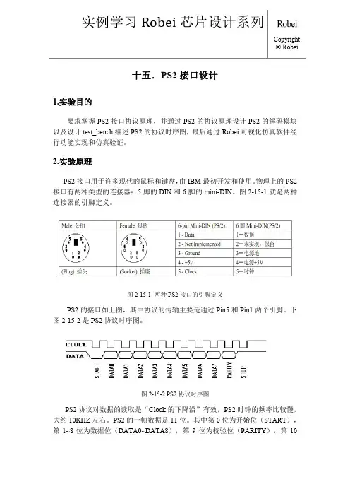
十五.PS2接口设计1.实验目的要求掌握PS2接口协议原理,并通过PS2的协议原理设计PS2的解码模块以及设计test_bench描述PS2的协议时序图,最后通过Robei可视化仿真软件经行功能实现和仿真验证。
2.实验原理PS2接口用于许多现代的鼠标和键盘,由IBM最初开发和使用。
物理上的PS2接口有两种类型的连接器:5脚的DIN和6脚的mini-DIN。
图2-15-1就是两种连接器的引脚定义。
图2-15-1 两种PS2接口的引脚定义PS2的接口如上图,其中协议的传输主要是通过Pin5和Pin1两个引脚。
下图2-15-2是PS2协议时序图。
图2-15-2 PS2协议时序图PS2协议对数据的读取是“Clock的下降沿”有效,PS2时钟的频率比较慢,大约10KHZ左右。
PS2的一帧数据是11位。
其中第0位为开始位(START),第1~8位为数据位(DATA0~DATA8),第9位为校验位(PARITY),第10位为结束位(STOP )。
但对PS2解码时,除了第1~8位数据位外,其余的位都可忽视。
下面主要以PS2接口在编码键盘的应用为例进行实验。
键盘的编码有“通码”和“段码”之分。
可以这样解释,“通码”是某按键“按下事件”,“段码”是某按键的“释放事件”。
假如,按下“W ”键,就会输出“0x1d ”的“通码”。
释放“W ”键,就会输出“0xF0 0x1d ”的“段码”。
限于篇幅,编码方式不再列出,读者可以在网上搜索。
下图2-15-3显示组成PS2接口的各个模块:ps2_clk_inh2l_sig ps2_data_outps2_data_in ps2_done_sig图2-15-3 PS2模块化设计detect_module 是电平检测模块,为了检测PS2时钟信号(ps2_clk_in )的“下降沿”,然后将下降沿信号(h2l_sig )输出。
ps2_decode_module 是PS2的解码模块,依据detect_module 输出的时钟下降沿信号(h2l_sig ),对每一帧(11位)数据进行解码和过滤,最后将一字节数据输出ps2_data ,然后ps2_done_sig 产生一个高脉冲,表示完成一次性的解码操作。
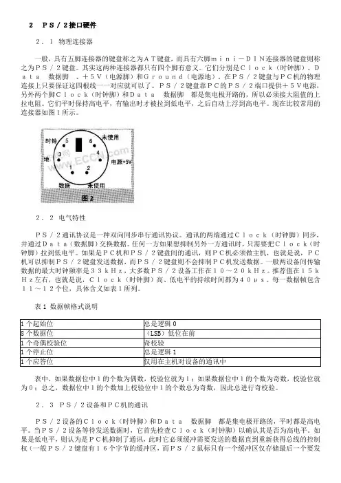
2PS/2接口硬件2.1物理连接器一般,具有五脚连接器的键盘称之为AT键盘,而具有六脚mini-DIN连接器的键盘则称之为PS/2键盘。
其实这两种连接器都只有四个脚有意义。
它们分别是Clock(时钟脚)、Data 数据脚 、+5V(电源脚)和Ground(电源地)。
在PS/2键盘与PC机的物理连接上只要保证这四根线一一对应就可以了。
PS/2键盘靠PC的PS/2端口提供+5V电源,另外两个脚Clock(时钟脚)和Data 数据脚 都是集电极开路的,所以必须接大阻值的上拉电阻。
它们平时保持高电平,有输出时才被拉到低电平,之后自动上浮到高电平。
现在比较常用的连接器如图1所示。
2.2电气特性PS/2通讯协议是一种双向同步串行通讯协议。
通讯的两端通过Clock(时钟脚)同步,并通过Data(数据脚)交换数据。
任何一方如果想抑制另外一方通讯时,只需要把Clock(时钟脚)拉到低电平。
如果是PC机和PS/2键盘间的通讯,则PC机必须做主机,也就是说,PC机可以抑制PS/2键盘发送数据,而PS/2键盘则不会抑制PC机发送数据。
一般两设备间传输数据的最大时钟频率是33kHz,大多数PS/2设备工作在10~20kHz。
推荐值在15kHz左右,也就是说,Clock(时钟脚)高、低电平的持续时间都为40μs。
每一数据帧包含11~12个位,具体含义如表1所列。
表1 数据帧格式说明表中,如果数据位中1的个数为偶数,校验位就为1;如果数据位中1的个数为奇数,校验位就为0;总之,数据位中1的个数加上校验位中1的个数总为奇数,因此总进行奇校验。
2.3PS/2设备和PC机的通讯PS/2设备的Clock(时钟脚)和Data 数据脚 都是集电极开路的,平时都是高电平。
当PS/2设备等待发送数据时,它首先检查Clock(时钟脚)以确认其是否为高电平。
如果是低电平,则认为是PC机抑制了通讯,此时它必须缓冲需要发送的数据直到重新获得总线的控制权(一般PS/2键盘有16个字节的缓冲区,而PS/2鼠标只有一个缓冲区仅存储最后一个要发送的数据)。
PS2键盘在单片机上的应用摘要:在嵌入式PC应用系统中,作为人机交互设备的键盘,往往采用结构简单按键少的矩阵键盘。
标准键盘虽然能直接与嵌入式PC机的PS/2接口相连,但是体积大,按键多,不能满足需求,本文提出用一种AT89C52单片机实现具有标准PS/2接口的矩阵键盘,具有便捷,实用的特点。
关键词:PS/2接口,PS/2键盘,拨号键,AT89C52,LCD1602Abstract:PS/2 interface is one of the most useful mouse interface.It was IBM’s patent named osulum before. It is the dedicate interface of mouse and keyboard. This text implied a plan using PS/2 to make a system. PS/2 tansmit the data which was pressed, and AT89C52 receive it ,disposed it and transmit it to Lcd1602. Lcd1602 discover it to make us know which key has been pressed. PS/2 simulate a phone’s dial keyboard. This system’s feature is the circuit is sample and useful.Keywords:PS/2 keyboard, AT89C52, LCD1602,PS/2 interface,dial keyboard目录1、前言 (1)2、整体方案设计 (2)2.1方案论证 (2)2.2方案比较 (3)3、单元模块设计 (4)3.1PS2键盘模块 (4)3.2单片机模块 (6)3.3LCD显示模块 (7)4、软件设计 (9)5、系统技术指标及精度和误差分析 (10)6、结论 (11)7、设计小结 (12)8、致谢 (14)9、参考文献 (14)附录1:电路总图 (15)附录2:仿真图 (16)附录3:软件代码 (17)1、前言单片机因其性价比高, 处理能力强, 且抗干扰能力好, 在医疗器械、机电液控制、数据传输等各类工控系统和设备仪器中得到广泛应用。
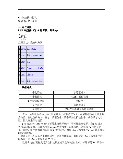
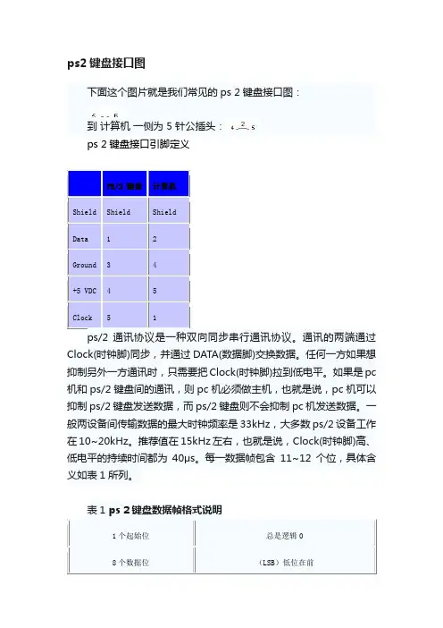
PS2键盘接口协议2009-06-03 16:11一.电气特性PS/2 键盘接口为 6 针母插,外观为:上图为接口底座引脚图1DATA Key Data2n/c Not connected3GND Gnd4VCC Power , +5 VDC5CLK Clock6n/c Not connected二.数据格式1个起始位总是逻辑08个数据位(LSB)低位在前1个奇偶校验位奇校验1个停止位总是逻辑11个应答位仅用在主机对设备的通讯中表中,如果数据位中1的个数为偶数,校验位就为1;如果数据位中1的个数为奇数,校验位就为0;总之,数据位中1的个数加上校验位中1的个数总为奇数,因此总进行奇校验。
ps2设备的clock和data都是集电极开路的,平时都是高电平。
当ps2设备等待发送数据时,它首先检查clock是否为高。
如果为低,则认为PC抑制了通讯,此时它缓冲数据直到获得总线的控制权。
如果clock为高电平,ps2则开始向PC发送数据。
一般都是由ps2设备产生时钟信号。
发送按帧格式。
数据位在clock为高电平时准备好,在clock下降沿被PC读入。
数据从键盘/鼠标发送到主机或从主机发送到键盘/鼠标,时钟都是PS2设备产生.主机对时钟控制有优先权,即主机想发送控制指令给PS2设备时,可以拉低时钟线至少100μS,然后再下拉数据线,最后释放时钟线为高。
PS2设备的时钟线和数据线都是集电极开路的,容易实现拉低电平。
PC在时钟的下降沿读取数据.PS: ps2协议是现在大多数鼠标,键盘与PC通讯的标准协议,鼠标的通讯更为简单些,只是传送的数据内容不一样而已。
三.数据发送时序键盘接口时序(a) 键盘发送时序;(b) 键盘接收时序从PS/2向PC机发送一个字节可按照下面的步骤进行:(1)检测时钟线电平,如果时钟线为低,则延时50μs;(2)检测判断时钟信号是否为高,为高,则向下执行,为低,则转到(1);(3)检测数据线是否为高,如果为高则继续执行,如果为低,则放弃发送(此时PC机在向PS/2设备发送数据,所以PS/2设备要转移到接收程序处接收数据);(4)延时20μs(如果此时正在发送起始位,则应延时40μs);(5)输出起始位(0)到数据线上。
第二章PS2键盘接口程序设计总结2.1 PS/2键盘接口简介键盘上包含了一个大型的按键矩阵,它们是由安装在电路板上的处理器(叫做“键盘编码器”)来监视的。
具体的处理器在键盘与键盘之间是多样化的,但是它们基本上都做着同样的事情:监视哪些按键被按下或释放了,并传送适当的数据到主机。
如果有必要,处理器处理所有的去抖动并在它的16 字节缓冲区里缓冲数据。
你的主板包含了一个“键盘控制器”,负责解码所有来自键盘的数据,并告诉你的软件什么事件发生了。
在主机和键盘之间的通讯使用IBM 的协议。
2.1.1 扫描码键盘的处理器花费很多的时间来扫描或监视按键矩阵。
如果它发现有键被按下、释放或按住,键盘将发送“扫描码”的信息包到计算机。
扫描码有两种不同的类型:“通码”和“断码”当一个键被按下或按住就发送通码;当一个键被释放就发送断码。
每个按键被分配了唯一的通码和断码,这样主机通过查找唯一的扫描码就可以测定是哪个按键。
每个键一整套的通断码组成了“扫描码集”。
有三套标准的扫描码集分别是第一套、第二套和第三套。
所有现代的键盘默认使用第二套扫描码。
2.1.2 通码、断码和机打重复率只要一个键被按下,这个键的通码就被发送到计算机。
记住通码只表示键盘上的一个按键,它不表示印刷在按键上的那个字符。
这就意味着在通码和ASCII 码之间没有已定义的关联。
直到主机把扫描码翻译成一个字符或命令。
虽然多数第二套通码都只有一个字节宽,但也有少数扩展按键的通码是两字节或四字节宽。
这类的通码第一个字节总是为“E0h”。
正如键按下通码就被发往计算机一样,只要键一释放断码就会被发送。
每个键都有它自己唯一的通码,它们也都有唯一的断码。
幸运的是你不用总是通过查表来找出按键的断码。
在通码和断码之间存在着必然的联系,多数第二套断码有两字节长它们的第一个字节是“F0h”,第二个字节是这个键的通码。
扩展按键的断码通常有三个字节,它们前两个字节是“E0h”,“F0h”,最后一个字节是这个按键通码的最后一个字节。
PS2 键盘接口设计之二(实现了从键盘输入并显示在
LCD 液晶屏上)
在熟悉了PS2 键盘接口设计之后,我想大家都希望将输入的数据在显示
屏中实时的显示出来或者看看我们到底输入的是什幺样的东西,基于这个原因,结合Spartan-3E 开发板上的资源,我利用了液晶1602 将输入的字符显示出来。
最终结果是可以从键盘上输入任意ASCII 字符,可以通过1602 显示
出来。
具体实现方法是基于我的上一篇博文上的PS2 键盘设计和修改后的1602 液晶接口,顶层文件定义如下图所示:
CapsLock 为大写锁定或者Shift 输入端,高有效,clk_50m 是系统时钟信号,ps2c,ps2d 为ps2 的时钟和数据端口定义,rst_n 为复位输入,低有效,disp_value 为输入字符的ASCII 值,sf_d 为LCD 数据端口,lcd_e,
lcd_rs,lcd_rs 为1602 控制信号。
具体包含两个模块:一个是键盘接口模块,一个是显示模块,键盘接口模块主要负责获取按键的ASCII 值,显示模块主要负责在LCD 上将该ASCII
值所代表的字符显示出来,具体定义如下所示:。
PS/2接口针脚定义图
2009年11月06日星期五 14:50 PS/2 键盘接口为 6 针母插,外观为:
DATA Key Data
Gnd
Power , +5 VDC
Clock
键盘接口引脚定义图
键盘接口为 5 针母插座:
PC/AT 键盘接口的引脚定义:
PC/XT 键盘接口的引脚定义稍有不同:
ps 2接口定义图
外观为:
母插引脚定义
DATA Key Data
Gnd
Power , +5 VDC
Clock
PS/2 6 针公插,外观为:
公插引脚定义
Key CLOCK
GND
DATA Key DATA
Power , +5 VDC
母座的PCB引脚
PS 2鼠标接口转串行鼠标转接器
PS 2键盘接口转普通键盘接口转接器
本转换口把一个普通键盘接到 PS/2 的键盘口上,PC 一侧为 6 针 PS/2 公插头:
到键盘一侧为 5 针母插头:
本转换口把一个串行鼠标接到 PS/2 鼠标口上,到鼠标一侧为 9 针公插头:
到 PC PS/2 鼠标口一侧为 6 针 PS/2 公插头:。
键盘接口设计1987年,IBM推出了ps/2键盘接口标准。
该标准定义了84~101键,采用6脚mini-DIN连接器。
一般,具有五脚连接器的键盘称之为AT键盘,而具有六脚mini-DIN连接器的键盘则称之为ps/2键盘。
其实这两种连接器都只有四个脚有意义。
它们分别是Clock(时钟脚)、DATA(数据脚)、+5V(电源脚)和Ground(电源地)。
在ps/2键盘与pc 机的物理连接上只要保证这四根线一一对应就可以了。
ps/2键盘靠pc的ps/2端口提供+5V电源,另外两个脚Clock(时钟脚)和DATA(数据脚)都是集电极开路的,所以必须接大阻值的上拉电阻。
它们平时保持高电平,有输出时才被拉到低电平,之后自动上浮到高电平。
现在比较常用的连接器如图1所示。
本实验基于FPGA用VHDL语言设计键盘接口,能够识别键盘输入的按键码,并通过实验箱上的发光灯显示接收到的数据。
PS/2协议PS/2采用11位的串行异步通信格式,这11位数据包括:起始位0、8位数据位(LSB在先)、奇校验位P、停止位1。
图2给出了键盘发送时序。
数据(KB_DAT)在时钟(KB_CLK)的上升沿改变,下降沿时有效,可被主机读取。
实验设计本实验根据PS/2协议。
识别键盘按下的按键,通过实验箱上的发光灯来显示扫描到的数据。
主要难点是要掌握PS/2的通信原理,然后再按照这个原理来识别键盘输入来的数据。
源程序如下:LIBRARY IEEE;USE IEEE.STD_LOGIC_1164.all;USE IEEE.STD_LOGIC_ARITH.all;USE IEEE.STD_LOGIC_UNSIGNED.all;ENTITY keyboard ISPORT( keyboard_clk, keyboard_data:in std_logic;clock,reset, read: in std_logic;scan_code: OUT STD_LOGIC_VECTOR(7 DOWNTO 0);scan_error: out STD_LOGIC;scan_ready: OUT STD_LOGIC);END keyboard;ARCHITECTURE a OF keyboard ISsignal in_code: STD_LOGIC_VECTOR(7 DOWNTO 0);SIGNAL INCNT: std_logic_vector(3 downto 0);SIGNAL SHIFTIN : std_logic_vector(7 downto 0);SIGNAL READ_CHAR : std_logic;SIGNAL INFLAG, ready_set,parity: std_logic;SIGNAL keyboard_clk_filtered : std_logic;SIGNAL filter : std_logic_vector(7 downto 0);BEGINPROCESS (read, ready_set)BEGINIF read = '1' THENscan_ready <= '0';ELSIF ready_set'EVENT and ready_set = '1' THENscan_ready <= '1';END IF;END PROCESS;--This process filters the raw clock signal coming from the keyboard using a shift --register and two AND gates Clock_filter:PROCESSBEGINWAIT UNTIL clock'EVENT AND clock= '1';filter (6 DOWNTO 0) <= filter(7 DOWNTO 1) ;filter(7) <= keyboard_clk;IF filter = "11111111" THENkeyboard_clk_filtered <= '1';ELSIF filter= "00000000" THENkeyboard_clk_filtered <= '0';END IF;END PROCESS ;-- Clock_filter;--This process reads in serial data coming from the terminal PROCESSBEGIN WAIT UNTIL (KEYBOARD_CLK_filtered'EVENT AND KEYBOARD_CLK_filtered='0');IF RESET='1' THENINCNT <= "0000";READ_CHAR <= '0';ELSEIF KEYBOARD_DATA='0' AND READ_CHAR='0' THENREAD_CHAR<= '1'; ready_set<= '0'; parity<='1';ELSE -- Shift in next 8 data bits to assemble a scan codeIF READ_CHAR = '1' and read='0' THENIF INCNT < "1000" THENINCNT <= INCNT + 1;SHIFTIN(6 DOWNTO 0) <= SHIFTIN(7 DOWNTO 1);SHIFTIN(7) <= KEYBOARD_DATA;parity<=parity xor keyboard_data;ready_set <= '0';elsif incnt="1000" thenif parity=keyboard_data thenscan_error<='0';elsescan_error<='1';end if;incnt<=incnt+1;ELSEin_code <= SHIFTIN(7 DOWNTO 0);READ_CHAR<='0';ready_set <= '1';INCNT <= "0000";END IF;END IF;END IF;END IF;END PROCESS;-- 7 3 0 7 3 0scan_code<="01100001" when in_code="00011100"else--A"01100010" when in_code="00110010"else--B"01100011" when in_code="00100001"else--C"01100100" when in_code="00100011"else--D"01100101" when in_code="00100100"else--E"01100110" when in_code="00101011"else--F"01100111" when in_code="00110100"else--G"01101000" when in_code="00110011"else--H"01101001" when in_code="01000011"else--I"01101010" when in_code="00111011"else--J"01101011" when in_code="01000010"else--K"01101100" when in_code="01001011"else--L"01101101" when in_code="00111010"else--M"01101110" when in_code="00110001"else--N"01101111" when in_code="01000100"else--O"01110000" when in_code="01001101"else--P"01110001" when in_code="00010101"else--Q"01110010" when in_code="00101101"else--R"01110011" when in_code="00011011"else--S"01110100" when in_code="00101100"else--T"01110101" when in_code="00111100"else--U"01110110" when in_code="00101010"else--V"01110111" when in_code="00011101"else--W"01111000" when in_code="00100010"else--X"01111001" when in_code="00110101"else--Y"01111010" when in_code="00011010"else--Z "00110000" when in_code="01000101"or in_code="01110000"else--0 "00110001" when in_code="00010110"or in_code="01101001"else--1"00110010" when in_code="00011110"or in_code="01110010"else--2"00110011" when in_code="00100110"or in_code="01111010"else--3"00110100" when in_code="00100101"or in_code="01101011"else--4"00110101" when in_code="01001110"or in_code="01110011"else--5"00110110" when in_code="00110110"or in_code="01110100"else--6 "00110111" when in_code="00111101"or in_code="01101100"else--7 "00111000" when in_code="00111110"or in_code="01110101"else--8"00111001" when in_code="01000110"or in_code="01111101"else--9 in_code;END a;按键说明:Reset->117 复位read->118 扫描允许信号keyboard_clk->125 键盘输入时钟keyboard_data->126 键盘输入数据scan_code->85..96 扫描得到的数据scan_error->75 扫描出错信息scan_ready->76 扫描完毕,可以接收下一次输入了操作方法:把程序下载到实验箱后,在键盘接口处插好键盘,把时钟频率调到4MHZ(也就是28管脚的第三个针脚。
第一章 PS/2鼠标键盘协议Introduction:引言The PS/2 device interface, used by many modern mice and keyboards, was developed by IBM and originally appeared in the IBM Technical Reference Manual. However, this document has not been printed for many years and as far as I know, there is currently no official publication of this information. I have not had access to the IBM Technical Reference Manual, so all information on this page comes from my own experiences as well as help from the references listed at the bottom of this page.PS/2设备接口用于许多现代的鼠标和键盘它是由IBM开发并且最初出现在IBM技术参考手册里但是当我知道的时候这篇文件就已经很多年没有印刷了因此关于这个内容现在没有官方的出版物我无法访问IBM的技术参考手册所以本网页中的所有信息都来自于我自己的经验及本页最下面列出的参考的帮助译者注这些参考的条目在本章的结尾处This document descibes the interface used by the PS/2 mouse, PS/2 keyboard, and AT keyboard. I'll cover the physical and electrical interface, as well as the protocol. If you need higher-level information, such as commands, data packet formats, or other information specific to the keyboard or mouse, I have written separate documents for the two devices:这个文件描述了用于PS/2鼠标PS/2键盘及AT键盘的接口我将论及物理和电气接口也包括协议如果你需要更高级的信息诸如命令数据包的格式或者其他关于键盘鼠标的特别细节那么我对这两种设备写了独立的文件The PS/2 (AT) Keyboard InterfaceThe PS/2 Mouse Interface译者注这两篇文章已经包含到这篇译文中来了是第二章和第三章I also encourage you to check out my homepage for more information related to this topic, including projects, code, and links related to the mouse and keyboard.我同样鼓励你在我的主页上校对更多与这个话题相关的信息包括工程代码和与鼠标键盘有关的链接The Connector:连接器The physical PS/2 port is one of two styles of connectors: The 5-pin DIN or the 6-pin mini-DIN. Both connectors are completely (electrically) similar; the only practical difference between the two is the arrangement of pins. This means the two types of connectors can easily be changed with simple hard-wired adaptors. These cost about $6 each or you can make your own by matching the pins on any two connectors. The DIN standard was created by the German Standardization Organization (Deutsches Institut fuer Norm) . Their website is at http://www.din.de/ (this site is in German, but most of their pages are also available in English.)物理上的PS/2端口是两类连接器中的一种5脚的DIN或6脚的mini-DIN这两种连接器在电气特性上是十分类似的实际上两者只有一点不同那就是管脚的排列这就意味着这两类连接器可以很容易用一种简单的硬件连线的适配器来转换这种适配器大约每个值6美元或者你可以根据任意两种连接器的对应管脚关系做你自己的适配器DIN标准是由德国标准化组织(Deutsches Institut fuer Norm)建立的他们的网站在http://www.din.de/这个站点是德文的但他们的很多网页同样可用于英文PC keyboards can have either a 6-pin mini-DIN or a 5-pin DIN connector. If your keyboard has a 6-pin mini-DIN and your computer has a 5-pin DIN (or visa versa), the two can be made compatible with the adaptors described above. Keyboards with the 6-pin mini-DIN are often referred to as "PS/2" keyboards, while those with the 5-pin DIN are called "AT" devices ("XT" keyboards also used the 5-pin DIN, but they are quite old and haven't been made for many years.) All modern keyboards built for the PC are either PS/2, AT, or USB. This document does not apply to USB devices, which use a completely different interface.PC键盘可以有6脚的mini-DIN或5脚的DIN连接器如果你的键盘是6脚的mini-DIN而你的计算机是5脚的DIN或者相反这两类连接器可以用上面提到的适配器来兼容具有6脚mini-DIN的键盘通常被叫做PS/2键盘而那些有5脚DIN叫做AT设备XT键盘也使用5脚DIN但它们非常古老并且多年前就不生产了所有现代的为PC建造的键盘不是PS/2,AT就是USB的这篇文章不适用于USB设备它们使用了一种完全不同的接口Mice come in a number of shapes and sizes (and interfaces.) The most popular type is probably the PS/2 mouse, with USB mice gaining popularity. Serial mice are also quite popular, but the computer industry is abandoning them in support of USB and PS/2 devices. This document applies only to PS/2 mice. If you want to interface a serial mouse, check out Microchip's appnote #519, "Implementing a Simple Serial Mouse Controller."鼠标流行着大量的形状和大小和接口最流行的类型可能算是PS/2鼠标现在USB鼠标渐渐开始流行起来了串行鼠标同样非常流行但计算机工业放弃了它们转而支持USB和PS/2设备这篇文章仅适用于PS/2鼠标如果你要知道一个串行鼠标的接口请查验Microchip的519号应用实现一个简单的串行鼠标控制器As a side note, there is one other type of connector you may run into on keyboards. While most keyboard cables are hard-wired to the keyboard, there are some whose cable is not permanently attached and come as a separate component. These cables have a DIN connector on one end (the end that connects to the computer) and a SDL (Sheilded Data Link) connector on the keyboard end. SDL was created by a company called "AMP." This connector is somewhat similar to a telephone connector in that it has wires and springs rather than pins, and a clip holds it in place. If you need more information on this connector, you might be able to find it on AMP's website at /. I have only seen this type of connector on (old) XT keyboards, although there may be AT keyboards that also use the SDL. Don't confuse the SDL connector with the USB connector--they probably both look similar in my diagram below, but they are actually very different. Keep in mind that the SDL connector has springs and moving parts, while the USB connector does not.作为边注还有另外一种类型的连接器你可以在键盘上碰到虽然多数键盘电缆都是固定连接到键盘的但还有一些键盘电缆不是永久挂接的而是作为一个单独的部件这种电缆在一端有一个DIN的连接器这端连接到计算机而连接到键盘的那一端是一个SDL屏蔽的数据连接器连接器SDL是由一个叫AMP的公司建立的这种连接器有点象电话连接器它有金属丝和弹簧代替管脚用一个卡子保持它在适当的位置上如果你需要知道关于这种连接器的更多信息你可以在AMP的网站找到它AMP的网站在/尽管可能AT键盘同样可以使用SDL但我只在一个很老的XT键盘上看见过这种连接器不要把SDL连接器和USB连接器混淆起来这两个可能在我下面画的示意图中看起来有点类似但是它们实际上是非常不同的记住SDL有弹簧和活动部件而USB连接器没有The pinouts for each connector are shown below:每种连接器的引脚定义如下所示母的5-pin DIN (AT/XT): 5脚DIN(AT/XT)Male 公的 Female1 - Clock 1时钟2 - Data 2数据3 - Not Implemented 3未实现保留4 - Ground 4电源地插座 5 - +5v 5电源+5V(Plug) 插头 (Socket)母的6-pin Mini-DIN (PS/2): 6脚Mini-DIN(PS/2) Male 公的 Female1 - Data 1数据2 - Not Implemented 2未实现保留3 - Ground 3电源地4 - +5v 4电源+5V插座 5 - Clock 5时钟(Plug) 插头 (Socket)6 - Not Implemented 6未实现保留6脚SDL6-pinSDL:A - Not Implemented A未实现保留B - Data B数据C - Ground C电源地D - Clock D时钟E - +5v E电源+5VF - Not Implemented F未实现保留General Description:一般性描述(Note: Throughout this document, I may use the more general term "host" to refer to the computer--or whatever the keyboard/mouse is connected to-- and the term "device" will refer to the keyboard/mouse.) 注意遍及这篇文章我使用了更普通的术语host使之计算机或者键盘/鼠标连接到的单元而术语device是指键盘/鼠标译者注下面的译文中host可能被翻译成主机There are four interesting pins on the connectors just described: Ground, +5v, Data, and Clock. The +5V is supplied by the host (computer) and the keyboard/mouse's ground is connected to the host's electrical ground. Data and Clock are both open collector, which means they are normally held at a high logic level but can easily be pulled down to ground (logic 0.) Any device you connect to a PS/2 mouse, keyboard, or host should have large pull-up resistors on the Clock and Data lines. You apply a "0" by pulling the line low and you apply a "1" by letting the line float high. Refer to Figure 1 for a general interface to Data and Clock. (Note: if you are going to use a microcontroller such as the PIC, where I/O is bidirectional, you may skip the transistors and buffers and use the same pin for both input and output. With this configuration, a "1" is asserted by setting the pin to input and let the resistor pull the line high. A "0" is then asserted by changing the pin to output and write a "0" to that pin, which will pull the line to ground.)在刚才提到连接器上有四个有趣的管脚电源地5V数据和时钟host计算机提供5V并且键盘/鼠标的地连接到host的电源地上数据和时钟都是集电极开路的这就意味着它们通常保持高电平而且很容易下拉到地逻辑0任何你连接到PS/2鼠标键盘或host的设备在时钟和数据线上要有一个大的上拉电阻置0就把线拉低置1就让线上浮成高电平参考图1中数据和时钟线的一般接口结构注意如果你打算使用象PIC这样的微控制器由于它们的I/O管脚是双向的你可以跳过晶体管和缓冲门并且通用同一个管脚进行输入和输出在这种组态情况下要设置管脚为输入就写入1使得电阻上拉线上的电平要改变管脚为输出就写入0到那个管脚把线路下拉到地Figure 1: Open-collector interface to Dataand Clock. Data and Clock are read on themicrocontroller's port A and B, respectively.Both lines are normally held at +5V, but canbe pulled to ground by asserting logic 1 onC and D. As a result, Data equals D,inverted, and Clock equals C, inverted.图1数据线和时钟线的集电极开路接口数据和时钟分别由微控制器的A端口和B端口读入这两条线通常保持+5V但可以往端口C和D写入1来拉到地结果是数据是D的反相时钟是C的反相The PS/2 mouse and keyboard implement a bidirectional synchronous serial protocol. In other words, Data is sent one bit at a time on the Data line and is read on each time Clock is pulsed. The keyboard/mouse can send data to the host and the host can send data to the device, but the host always has priority over the bus and can inhibit communication from the keyboard/mouse at any time by holding Clock low.PS/2鼠标和键盘履行一种双向同步串行协议换句话说每次数据线上发送一位数据并且每在时钟线上发一个脉冲就被读入键盘/鼠标可以发送数据到主机而主机也可以发送数据到设备但主机总是在总线上有优先权它可以在任何时候抑制来自于键盘/鼠标的通讯只要把时钟拉低即可Data sent from the keyboard/mouse to the host is read on the falling edge of the clock signal (when Clock goes from high to low); data sent from the host to the keyboard/mouse is read on the rising edge (when Clock goes from low to high.) Regardless of the direction of communication, the keyboard/mouse always generates the clock signal. If the host wants to send data, it must first tell the device to start generating a clock signal (that process is described in the next section.) The maximum clock frequency is 33 kHz and most devices operate within 10-20kHz. If you want to build a PS/2 device, I would recommend keeping this frequency around 15 kHz. This means Clock should be high for about 40 microseconds and low for 40 microseconds.从键盘/鼠标发送到主机的数据在时钟信号的下降沿当时钟从高变到低的时候被读取从主机发送到键盘/鼠标的数据在上升沿当时钟从低变到高的时候被读取不管通讯的方向怎样键盘/鼠标总是产生时钟信号如果主机要发送数据它必须首先告诉设备开始产生时钟信号这个过程在下一章节中被描述最大的时钟频率是33kHz而且大多数设备工作在1020kHz如果你要制作一个PS/2设备我推荐你把频率控制在15kHz左右这就意味着时钟应该是高40微秒低40微秒All data is arranged in bytes with each byte sent in a frame consisting of 11-12 bits. These bits are:所有数据安排在字节中每个字节为一帧包含了1112个位这些位的含义如下1 start bit. This is always 0. 1个起始位总是为08 data bits, least significant bit first. 8个数据位低位在前1 parity bit (odd parity). 1个校验位奇校验1 stop bit. This is always 1. 1个停止位总是为11 acknowledge bit (Host-to-device communication only) 1个应答位仅在主机对设备的通讯中The parity bit is set if there is an even number of 1's in the data bits and reset (0) if there is an odd number of 1's in the data bits. The number of 1's in the data bits plus the parity bit always add up to an odd number (odd parity.) This is used for error detection.如果数据位中包含偶数个1校验位就会置1如果数据位中包含奇数个1校验位就会置0数据位中1的个数加上校验位总为奇数这就是奇校验这是用来错误检测When the host is sending data to the keyboard/mouse, a handshaking bit is sent from the device to acknowledge the packet was received. This bit is not present when the device sends data to the host.当主机发送数据给键盘/鼠标时设备回送一个握手信号来应答数据包已经收到这个位不会出现在设备发送数据到主机的过程中Device-to-Host Communication:设备到主机的通讯过程The Data and Clock lines are both open collector (normally held at a high logic level.) When the keyboard or mouse wants to send information, it first checks Clock to make sure it's at a high logic level. If it's not, the host is inhibiting communication and the device must buffer any to-be-sent data until it regains control of the bus (the keyboard has a 16-byte buffer and the mouse's buffer stores only the last packet sent.) If the Clock line is high, the device can begin to transmit its data.数据和时钟线都是集电极开路结构正常保持高电平当键盘或鼠标等待发送数据时它首先检查时钟以确认它是否是高电平如果不是那么是主机抑制了通讯设备必须缓冲任何要发送的数据直到重新获得总线的控制权键盘有16字节的缓冲区而鼠标的缓冲区仅存储最后一个要发送的数据包如果时钟线是高电平设备就可以开始传送数据As I mentioned in the previous section, the keyboard and mouse use a serial protocol consisting of 11-bit frames. These bits are:如我在上一节提及的键盘和鼠标使用一种每帧包含11位的串行协议这些位含义是1 start bit. This is always 0. 1个起始位总是为08 data bits, least significant bit first. 8个数据位低位在前1 parity bit (odd parity). 1个校验位奇校验1 stop bit. This is always 1. 1个停止位总是为1Each bit is read by the host on the falling edge of the clock, as is illustrated in Figures 2 & 3.每位在时钟的下降沿被主机读入如图2和3所示Figure 2: Device-to-hostcommunication. The Dataline changes state when Clockis high and that data is latchedon the falling edge of the clocksignal.图2设备到主机的通讯当时钟为高数据线改变状态在时钟信号的下降沿数据被锁存Figure 3: Scan code for the "Q"key (15h) being sent from akeyboard to the computer.Channel A is the Clock signal;channel B is the Data signal.图3Q键的扫描码从键盘发送到计算机通道A是时钟信号通道B是数据信号The clock frequency is 10-16.7kHz.The time from the rising edge of aclock pulse to a Data transitionshould be at least 5 microseconds. The time from a data transition to the falling edge of a clock pulse should be at least 5 microseconds and no greater than 25 microseconds. This timing is very important--you should follow it exactly. The host may pull the line low before the 11th clock pulse (stop bit), causing the device to abort sending the current byte (this is very rare.) After the stop bit is transmitted, the device should wait at least 50 microseconds before sending the next packet. This gives the host time to inhibit transmission while it processes the received byte (the host will usually automatically do this after each packet is received.) The device should wait at least 50 microseconds after the host releases an inhibit before sending any data.时钟频率为1016.7kHz从时钟脉冲的上升沿到一个数据转变的时间至少要有5微秒数据变化到时钟脉冲的下降沿的时间至少要有5微秒并且不大于25微秒这个定时非常重要你应该严格遵循它主机可以在第11个时钟脉冲停止位之前把线拉低导致设备放弃发送当前字节这是非常罕见的在停止位发送后设备在发送下个包前至少应该等待50毫秒这将给主机时间当它处理接收到的字节时抑制发送主机在收到每个包时通常自动做这个在主机释放抑制后设备至少应该在发送任何数据前等50毫秒I would recommend the following process for sending a single byte from an emulated keyboard/mouse to the host:我推荐下面的过程发送一个单一字节从仿真键盘/鼠标到主机1) Wait for Clock = high.2) Delay 50 microseconds.3) Clock still = high?No--goto step 14) Data =high?No--Abort (and read byte from host)5) Delay 20 microseconds (=40 microseconds to the time Clock is pulled low in sending the start bit.)6) Output Start bit (0) \ After sending each of these bits, test7) Output 8 data bits > Clock to make sure host hasn't pulled it8) Output Parity bit / low (which would abort this transmission.)9) Output Stop bit (1)10) Delay 30 microseconds (=50 microseconds from the time Clock is released in sending the stop bit)1) 等待Clock = high2) 延时 50 微秒3) Clock s仍旧为 high?No—到第1 步4) Data =high?No—放弃(并且从主机读取字节)5) 延迟 20 毫秒 (=40微秒to the time Clock is pulled low in sending the start bit.)6) 输出起始位(0) \ 在发送所有这些位的每一位后7) 输出8个数据位> 测试时钟确认主机是否把它拉低了8) 输出校验位/ 这说明主机要放弃这次传送9) 输出停止位 (1)10) 延迟30 毫秒 (=50微秒from the time Clock is released in sending the stop bit)The process for sending a single bit should then be as follows:按如下的过程发送单个位1) Set/Reset Data2) Delay 20 microseconds3) Bring Clock low4) Delay 40 microseconds5) Release Clock6) Delay 20 microseconds1) 设置/复位数据2) 延迟20 微秒3) 把时钟拉低4) 延迟40 微秒5) 释放时钟6) 延迟20 微秒Here is some sample code written for the PIC16F84 that follows the above algorithms to send a byte to the host. "Delay" is a self-explanitory macro; "CLOCK" and "DATA" are the bits connected to the Clock and Data lines; "TEMP0", "PARITY", and "COUNTER" are all general purpose registers. Note that in the "PS2outBit" routine, the Data and Clock lines are brought low by setting the appropriate I/O pin to output (it's assumed their output was set to "0" at the beginning of the program.) And they are allowed to float (high) by setting the I/O pin to input (and allow a pull-up resistor to pull the line high.) This was written for a PIC running at 4.61 MHz +/- 25% (RC oscillator: 5k/20pF). This is very important for timing considerations.这里有一些采用上面算法来发送一个字节到主机的PIC16F84的简单样例代码Delay是一自说明宏CLOCK和DATA是连接到时钟和数据线上的位单元TEMP0PARITY和COUNTER都是一般目的的寄存器注意在PS2outBit例程中数据线和时钟线通过设置适当的I/O脚为输出态来拉低电平在程序的开始它们的输出被置为0通过置I/O脚为输出它们就允许上浮为高电平允许上来电阻拉线路为高电平下面给PIC用的代码运行于4.61MHz +/-25%RC振荡器5k/20pF这个值对定时条件非常重要ByteOut movwf TEMP0 ;Save to-be-sent byteInhibitLoop btfss CLOCK ;Check for inhibitgoto InhibitLoopDelay 50 ;Delay 50 microsecondsbtfss CLOCK ;Check again for inhibit goto InhibitLoopbtfss DATA ;Check for request-to-sendretlw 0xFFclrf PARITY ;Init reg for parity calcmovlw 0x08movwf COUNTERmovlw 0x00call BitOut ;Output Start bit (0)btfss CLOCK ;Test for inhibitgoto ByteOutEndDelay 4ByteOutLoop movf TEMP0, wxorwf PARITY, f ;Calculate paritycall BitOut ;Output Data bitsbtfss CLOCK ;Test for inhibitgoto ByteOutEndrrf TEMP0, fdecfsz COUNTER, fgoto ByteOutLoopDelay 2comf PARITY, wcall BitOut ;Output Parity bitbtfss CLOCK ;Test for inhibitgoto ByteOutEndDelay 5movlw 0xFFcall BitOut ;Output Stop bit (1)Delay 48retlw 0x00ByteOutEnd bsf STATUS, RP0 ;Host has abortedbsf DATA ;DATA=1bsf CLOCK ;CLOCK=1bcf STATUS, RP0retlw 0xFEBitOut bsf STATUS, RP0andlw 0x01btfss STATUS, Zbsf DATAbtfsc STATUS, Zbcf DATADelay 21bcf CLOCKDelay 45bsf CLOCKbcf STATUS, RP0Delay 5returnHost to Device Communication:主机到设备的通讯The packet is sent a little differently in host-to-device communication...被发送的包有点不同于主机到设备通讯过程First of all, the PS/2 device always generates the clock signal. If the host wants to send data, it must first put the Clock and Data lines in a "Request-to-send" state as follows:首先PS/2设备总是产生时钟信号如果主机要发送数据它必须首先把时钟和数据线设置为请求发送状态如下示Inhibit communication by pulling Clock low for at least 100 microseconds.通过下拉时钟线至少100微秒来抑制通讯Apply "Request-to-send" by pulling Data low, then release Clock.通过下拉数据线来应用请求发送然后释放时钟The device should check for this state at intervals not to exceed 10 milliseconds. When the device detects this state, it will begin generating Clock signals and clock in eight data bits and one stop bit. The host changes the Data line only when the Clock line is low, and data is latched on the rising edge of the clock pulse. This is opposite of what occours in device-to-host communication.设备应该在不超过10毫秒的间隔内就要检查这个状态当设备检测到这个状态它将开始产生时钟信号并且时钟脉冲标记下输入八个数据位和一个停止位主机仅当时钟线为低的时候改变数据线而数据在时钟脉冲的上升沿被锁存这在发生在设备到主机通讯的过程中正好相反After the stop bit is sent, the device will acknowledge the received byte by bringing the Data line low and generating one last clock pulse. If the host does not release the Data line after the 11th clock pulse, the device will continue to generate clock pulses until the the Data line is released (the device will then generate an error.) 在停止位发送后设备要应答接收到的字节就把数据线拉低并产生最后一个时钟脉冲如果主机在第11个时钟脉冲后不释放数据线设备将继续产生时钟脉冲直到数据线被释放然后设备将产生一个错误The Host may abort transmission at time before the 11th clock pulse (acknowledge bit) by holding Clock low for at least 100 microseconds.主机可以在第11个时钟脉冲应答位前中止一次传送只要下拉时钟线至少100微秒To make this process a little easier to understand, here's the steps the host must follow to send data to a PS/2 device:要使得这个过程易于理解主机必须按下面的步骤发送数据到PS/2设备1) Bring the Clock line low for at least 100 microseconds.2) Bring the Data line low.3) Release the Clock line.4) Wait for the device to bring the Clock line low.5) Set/reset the Data line to send the first data bit6) Wait for the device to bring Clock high.7) Wait for the device to bring Clock low.8) Repeat steps 5-7 for the other seven data bits and the parity bit9) Release the Data line.10) Wait for the device to bring Data low.11) Wait for the device to bring Clock low.12) Wait for the device to release Data and Clock1) 把时钟线拉低至少100微秒2) 把数据线拉低3) 释放数据线4) 等待设备把时钟线拉低5) 设置/复位数据线发送第一个数据位6) 等待设备把时钟拉高7) 等待设备把时钟拉低8) 重复 5-7步发送剩下的7个数据位和校验位9) 释放数据线10) 等待设备把数据线拉低11) 等待设备把时钟线拉低12) 等待设备释放数据线和时钟线Figure 3 shows this graphically and Figure 4 separates the timing to show which signals are generated by the host, and which are generated by the PS/2 device. Notice the change in timing for the Ack bit--the data transition occours when the Clock line is high (rather than when it is low as is the case for the other 11 bits.)图3用图形表示图4以单独的时序表示了由主机产生的信号及由PS/2设备产生的信号注意应答位时序的改变数据改变发生在时钟线为高的时候不同于其它11位是当它为低的时候Figure 3: Host-to-Device Communication.图3主机到设备的通讯Figure 4: Detailed host-to-device communication.图4主机到设备通讯的详细过程Figure 4 shows two important timing considerations: (a), and (b). (a), the time it takes the device to begin generating clock pulses after the host initially takes the Clock line low, must be no greater than 15ms; (b), the time it takes for the packet to be sent, must be no greater than 2ms. If either of these time limits is not met, the host will generate an error. Immediately after the packet is received, the host may bring the Clock line low to inhibit communication while it processes data. If the command sent by the host requires a response, that response must be received no later than 20ms after the host releases the Clock line. If this does not happen, the host generates an error. As was the case with Device-to-host communication, no Data transition may occur with 5 microseconds of a Clock transition.图4描述了两个重要的定时条件a和b a在主机最初把书记现拉低后设备开始产生时钟脉冲的时间必须步大于15ms b数据包被发送的时间必须不大于2ms如果这两个条件不满足主机将产生一个错误在包收到后主机为了处理数据立刻把时钟线拉低来抑制通讯如果主机发送的命令要求有一个回应这个回应必须在书籍释放时钟线后20ms之内被收到如果没有收到则主机产生一个错误在设备到主机通讯的情况中时钟改变后的5微秒内不应该发生数据改变的情况If you want to emulate a mouse or keyboard, I would recommend reading data from the host as follows:如果呢要仿真一个鼠标或键盘我推荐你按如下的过程从主机读入数据In your main program, check for Data=low at least every 10 milliseconds.If Data has been brought low by the host, read one byte from the host在你的主程序中至少每10毫秒检测数据线是否为低如果数据线已被主机拉低则从主机读取一个字节1) Wait for Clock=high2) Is Data still low?No--An error occurred; Abort.3) Read 8 data bits \ After reading each of these bits, test4) Read parity bit > Clock to make sure host hasn't pulled it5) Read stop bit / low (which would abort this transmission.)6) Data still equals 0?Yes--Keep clocking until Data=1 then generate an error7) Output Acknowledge bit8) Check Parity bit.Generate an error if parity bit is incorrect9) Delay 45 microseconds (to give host time to inhibit next transmission.)1) 等待时钟线为高2) 数据线仍然为低吗不有错误发生放弃3) 读入8个数据位\ 在读入这些位后4) 读入校验位> 测试时钟线数否被主机拉低5) 读入停止位/ 这就意味着放弃这次传送6) 数据线仍旧为0吗是保持时钟直到数据1然后产生一个错误7) 输出应答位8) 检查校验位如果校验位不正确则产生一个错误9) 延迟45 微秒给主机时间抑制下次的传送Read each bit (8 data bits, parity bit, and stop bit) as follows:1) Delay 20 microseconds2) Bring Clock low3) Delay 40 microseconds4) Release Clock5) Delay 20 microsecond6) Read Data line按如下次序读取每位8个数据位检验位和停止位1) 延迟 20 微秒2) 把时钟拉低3) 延迟 40 微秒4) 释放时钟5) 延迟20 微秒7) 读数据线Send the acknowledge bit as follows:1) Delay 15 microseconds2) Bring Data low3) Delay 5 microseconds4) Bring Clock low5) Delay 40 microseconds6) Release Clock7) Delay 5 microseconds8) Release Data按如下次序发送应答位1) 延迟15 微秒2) 把数据线拉低3) 延迟5 微秒4) 把时钟线拉低5) 延迟40 微秒6) 释放时钟线7) 延迟5 微秒8) 释放数据线Here is some sample code written for the PIC16F84 that implements the above algorithms to read data from a PS/2 host. "Delay" is a self-explanitory macro; "CLOCK" and "DATA" are the port bits connected to the Clock and Data lines; "TEMP0", "PARITY", and "COUNTER" are all general purpose registers. Note that in the "PS2inBit" routine, Clock is brought low by setting the appropriate I/O pin to output (it's assumed they were set to "0" at the beginning of the program.) And it is allowed to float (high) by setting the I/O pin to input (and allow a pull-up resistor to pull the line high.) Timing was worked out for a PIC running at 4.61 MHz +/- 25% (RC oscillator with values 5k/20 pF). Will work for any oscillator between 3.50 MHz - 5.76 MHz.这里有写给PIC16F84的样例实现了上述从PS/2主机读取数据的算法Delay是一个自扩展宏CLOCK和DATA是连接到时钟线和数据线上的位端口TEMP0PARITY和COUNTER都是一般用途的寄存器注意在PS2inBit例程中置适当的I/O脚为输出来把时钟拉低在程序的开始处它们被设置为0置I/O脚为输入就是让它们上浮成高电平上拉电阻把管线拉成高电平为达到设计的定时时序PIC应运行于4.61MHz +/-25%RC振荡器的值是5k/20pF当然也可以工作于任何3.50MHz 5.76MHz的振荡器ByteIn btfss CLOCK ;Wait for start bitgoto ByteInbtfsc DATAgoto ByteInmovlw 0x08movwf COUNTERclrf PARITY ;Init reg for parity calcDelay 28ByteInLoop call BitIn ;Clock in Data bitsbtfss CLOCK ;Test for inhibitretlw 0xFEbcf STATUS, Crrf RECEIVE, fiorwf RECEIVE, fxorwf PARITY,fdecfsz COUNTER, fgoto ByteInLoopDelay 1call BitIn ;Clock in Parity bitbtfss CLOCK ;Test for inhibitretlw 0xFExorwf PARITY, fDelay 5ByteInLoop1 Delay 1call BitIn ;Clock in Stop bitbtfss CLOCK ;Test for inhibitretlw 0xFExorlw 0x00btfsc STATUS, Z ;Stop bit = 1?clrf PARITY No--cause an error condition.btfsc STATUS, Z ;Stop bit = 1?goto ByteInLoop1 ; No--keep clocking.bsf STATUS, RP0 ;Acknowledgebcf DATADelay 11bcf CLOCKDelay 45bsf CLOCKDelay 7bsf DATAbcf STATUS, RP0btfss PARITY, 7 ;Parity correct?retlw 0xFF ; No--return errorDelay 45retlw 0x00BitIn Delay 8bsf STATUS, RP0bcf CLOCKDelay 45bsf CLOCKbcf STATUS, RP0Delay 21btfsc DATAretlw 0x80retlw 0x00Other Sources / References:其它资源和参考Adam's micro-Resources Home - Many pages/links to related information.The AT Keyboard - My page on AT keyboardsThe PS/2 Mouse - My page on the PS/2 mouseSynaptics Touchpad Interfacing Guide -Very informative!PS/2 Keyboard and Mouse Protocols - Timing diagrams.Holtek - Informative datasheets on many different PS/2 mice (and other peripherals). More Links - Many more links to related resources.。