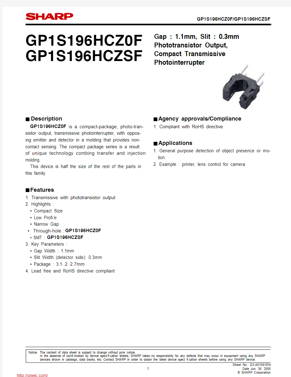
GP1S196HCZ0F GP1S196HCZSF Gap : 1.1mm, Slit : 0.3mm Phototransistor Output, Compact Transmissive Photointerrupter
■Description
GP1S196HCZ0F is a compact-package, photo-tran-sistor output, transmissive photointerrupter, with oppos-ing emitter and detector in a molding that provides non-contact sensing. The compact package series is a result of unique technology combing transfer and injection molding.
This device is half the size of the rest of the parts in this family.
■Features
1. Transmissive with phototransistor output
2. Highlights :
? Compact Size
? Low Pro? le
? Narrow Gap
? Through-hole : GP1S196HCZ0F
? SMT : GP1S196HCZSF
3. Key Parameters :
? Gap Width : 1.1mm
? Slit Width (detector side): 0.3mm
? Package : 3.1×2×2.7mm
4. Lead free and RoHS directive compliant
■Agency approvals/Compliance
1. Compliant with RoHS directive
■Applications
1. General purpose detection of object presence or mo-tion.
2. Example : printer, lens control for camera
Notice The content of data sheet is subject to change without prior notice.
In the absence of con? rmation by device speci? cation sheets, SHARP takes no responsibility for any defects that may occur in equipment using any SHARP
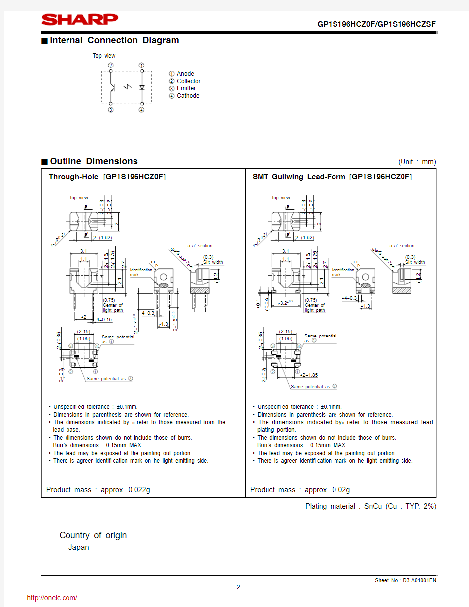
■Internal Connection Diagram
■Outline Dimensions
(Unit : mm)
Plating material : SnCu (Cu : TYP . 2%)
Top view
Anode Collector Emitter Cathode
Country of origin
Japan
■Absolute Maximum Ratings
■Electro-optical Characteristics (T a=25?C )
Parameter Symbol Rating Unit
Input Forward current I F30mA Reverse voltage V R6V Power dissipation P75mW
Output Collector-emitter voltage V CEO35V Emitter-collector voltage V ECO6V Collector current I C20mA Collector power dissipation P C75mW
Total power dissipation P tot100mW
Operating temperature T opr?25 to +85?C
Storage temperature T stg?40 to +100?C
?1Soldering temperature T
sol
260?C
?1 For 3s or less
(T a=25?C ) Parameter Symbol Condition MIN.TYP.MAX.Unit
Input Forward voltage V F I F=20mA? 1.2 1.4V Reverse current I R V R=3V??10μA
Output Collector dark current I CEO V CE=20V??100nA
Transfer charac-teristics Collector current I C V CE=5V, I F=5mA100?400μA Collector-emitter saturation voltage V CE(sat)I F=10mA, I C=40μA??0.4V
Response time
Rise time t r
V CE=5V, I C=100μA, R L=1kΩ
?50150
μs Fall time t f?50
150
(GP1S196HCZ0F)
Fig.5 Collector Current vs. Collector- emitter Voltage
Fig.6 Relative Collector Current vs.
Ambient Temperature
Fig.3 Forward Current vs. Forward
Voltage
Fig.4 Collector Current vs. Forward Current
10
100
1
F o r w a r d c u r r e n t I F (m A )
Forward voltage V F (V)
Forward current I F (mA)
11.10.90.80.70.60.50.40.30.20.1
C o l l e c t o r c u r r e n t I C (m A )
2
1.61.20.8
0.4
C o l l e c t o r c u r r e n t I C (m A )
Collector-emitter voltage V CE (V)
R e l a t i v e c o l l e c t
o r c u r r e n t (%)
Ambient temperature T a (C)
0130120110100908070605040302010
Fig.1 Forward Current vs. Ambient Temperature
Fig.2 Power Dissipation vs. Ambient Temperature
0605040302010 25
025*********
F o r w a r d c u r r e n t I F (m A )
Ambient temperature T a (?C) 0604080
100120
20P o w e r d i s s i p a t i o n P , P c , P t o t (m W )
Ambient temperature T a (?C)
7515
Fig.7 Collector-emitter Saturation Votage vs. Ambient Temperature
Fig.8 Collector Dark Current vs. Ambient Temperature
Fig.9 Response Time vs. Load Resistance
Fig.10 Test Circuit for Response Time
Fig.11 Relative Collector Current vs. Shield Distance (1)
Fig.12 Relative Collector Current vs. Shield Distance (1)
C o l l e c t o r -e m i t t e r s a t u r a t i o n v o l t a g e V C E (s a t ) (V )
Ambient temperature T a (?C)
0.20.180.160.140.120.10.080.060.04
0.1
1 000
10
1100
R e s p o n s e t i m e (μs )
Load resistance R L (k Ω)
10 10
10 9
10 7
10 6
10 8
C o l l e c t o r d a r k c u r r e n t I C E O (A )
Ambient temperature T a (?C)
R e l a t i v e c o l l e c t o r c u r r e n t (%)
10020304050609010070800
0.5
1
1.5
2Shield moving distance L (mm)
R e l a t i v e c
o l l e c t o r c u r r e n t (%)
10020304050609010070800
0.5
1
1.5
2Shield moving distance L (mm)
Remarks : Please be aware that all data in the graph are just for reference and not for guarantee.
■Design Considerations ●Design guide
1) Prevention of detection error
To prevent photointerrupter from faulty operation caused by external light, do not set the detecting face to the external light.
2) Position of opaque board
Opaque board shall be installed at place 1.4mm or more from the top of elements.(Example)
This product is not designed against irradiation and incorporates non-coherent IRED.
●Degradation
In general, the emission of the IRED used in photointerrupter will degrade over time.
In the case of long term operation, please take the general IRED degradation (50% degradation over 5 years) into the design consideration.
●Recommended Foot Print (Only for GP1S196HCZSF
)
1.4mm or more
●Parts
This product is assembled using the below parts.? Photodetector (qty. : 1)
Category Material Maximum Sensitivity
wavelength (nm)
Sensitivity
wavelength (nm)
Response time (μs)
Phototransistor Silicon (Si)930700 to 1 20020? Photo emitter (qty. : 1)
Category Material Maximum light emitting
wavelength (nm)
I/O Frequency (MHz)
Infrared emitting diode
(non-coherent)
Gallium arsenide (GaAs)9500.3 ? Material
Case Lead frame Lead frame plating
Black polyphernylene
sul? de resin (UL94 V-0)
42Alloy SnCu plating
■Manufacturing Guidelines
●Storage and management after open (Only for GP1S196HCZSF)
Storage condition
Storage temp.: 5 to 30?C, Storage humidity : 70%RH or less at regular packaging.
Treatment after opening the moisture-proof package
After opening, you should mount the products while keeping them on the condition of 5 to 25?C and 70%RH or less in humidity within 4 days.
After opening the bag once even if the prolonged storage is necessary, you should mount the products within two weeks.
And when you store the rest of products you should put into a DRY BOX. Otherwise after the rest of products and silicagel are sealed up again, you should keep them under the condition of 5 to 30?C and 70%RH or less in humidity.
Baking before mounting
When the above-mentioned storage method could not be executed, please process the baking treatment before mounting the products.
However the baking treatment is permitted within one time.
Recommended condition : 125?C, 16 to 24 hours
?Do not process the baking treatment with the product wrapped. When the baking treatment processing, you should move the products to a metallic tray or ? x temporarily the products to substrate.
●Soldering Method
Re? ow Soldering (Only for GP1S196HCZSF) :
Re? ow soldering should follow the temperature pro? le shown below.
Soldering should not exceed the curve of temperature pro? le and time.
Please solder within one time.
MAX
200?C
MAX
160?C
25?C
Flow Soldering:
Soldering should be completed below 260?C and within 3 s.
Please solder within one time.
Soldering area is 0.3mm or more away from the bottom of housing.
Please take care not to let any external force exert on lead pins.
Please don't do soldering with preheating, and please don't do soldering by re? ow.
Other notice
Please test the soldering method in actual condition and make sure the soldering works fine, since the impact on the junction between the device and PCB varies depending on the cooling and soldering conditions.
●Cleaning instructions
Solvent cleaning :
Solvent temperature should be 45?C or below. Immersion time should be 3 minutes or less.
Ultrasonic cleaning :
Do not execute ultrasonic cleaning.
Recommended solvent materials :
Ethyl alcohol, Methyl alcohol and Isopropyl alcohol.
●Presence of ODC
This product shall not contain the following materials.
And they are not used in the production process for this product.
Regulation substances : CFCs, Halon, Carbon tetrachloride, 1.1.1-Trichloroethane (Methylchloroform)
Speci? c brominated ? ame retardants such as the PBBOs and PBBs are not used in this product at all.
This product shall not contain the following materials banned in the RoHS Directive (2002/95/EC).
?Lead, Mercury, Cadmium, Hexavalent chromium, Polybrominated biphenyls (PBB), Polybrominated
diphenyl ethers (PBDE).
■Package speci? cation
●Sleeve package
1. Through-hole (GP1S196HCZ0F)
Package materials
Sleeve : Polycarbonate
Stopper : Styrene-Elastomer
Package method
MAX. 200 pcs. of products shall be packaged in a sleeve. Both ends shall be closed by tabbed and tabless stoppers.
MAX. 50 sleeves in one case.
2. SMT Gullwing (GP1S196HCZSF)
Package materials
Sleeve : Polycarbonate
Stopper : Styrene-Elastomer
Aluminium laminated Bag : Nylon, Polyphernylene, Aluminium
Package method
MAX. 200 pcs. of products shall be packaged in a sleeve. Both ends shall be closed by tabbed and tabless stoppers.
MAX. 50 sleeves with silicagel are enclosed in aluminium laminated bag. After sealing up the bag, it encased in one case.
分销商库存信息:
SHARP-MICROELECTRONICS
GP1S196HCZSF GP1S196HCZ0F