Evaluate: MAX2361/MAX2363/MAX2365
MAX2361/MAX2363W Evaluation Kits
________________________________________________________________Maxim Integrated Products 1
For pricing, delivery, and ordering information,please contact Maxim/Dallas Direct!at 1-888-629-4642, or visit Maxim’s website at https://www.doczj.com/doc/147035954.html,.
General Description
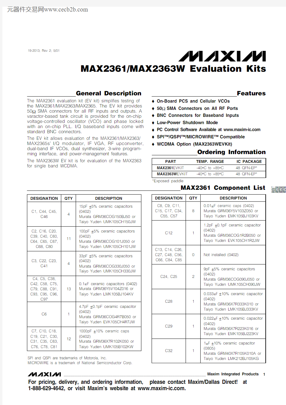
The MAX2361 evaluation kit (EV kit) simplifies testing of the MAX2361/MAX2363/MAX2365.The EV kit provides 50?SMA connectors for all RF inputs and outputs. A varactor-based tank circuit is provided for the on-chip voltage-controlled oscillator (VCO) and phase locked with an on-chip PLL. I/Q baseband inputs come with standard BNC connectors.
The EV kit allows evaluation of the MAX2361/MAX2363/MAX2365s’ I/Q modulator, IF VGA, RF upconverter,dual-band IF VCOs, dual synthesizer, 3-wire program-ming interface, and power-management features.
The MAX2363W EV kit is for evaluation of the MAX2363for single band WCDMA.
Features
o On-Board PCS and Cellular VCOs o 50?SMA Connectors on All RF Ports o BNC Connectors for Baseband Inputs o Low-Power Shutdown Mode
o PC Control Software Available at https://www.doczj.com/doc/147035954.html, o SPI?/QSPI?/MICROWIRE?Compatible o WCDMA Option (MAX2363WEVKit)
19-2013; Rev 2; 5/01
Ordering Information
*Exposed paddle
E v a l u a t e : M A X 2361/M A X 2363/M A X 2365
MAX2361/MAX2363W Evaluation Kits 2_______________________________________________________________________________________
Evaluate: MAX2361/MAX2363/MAX2365
MAX2361/MAX2363W Evaluation Kits
_______________________________________________________________________________________3
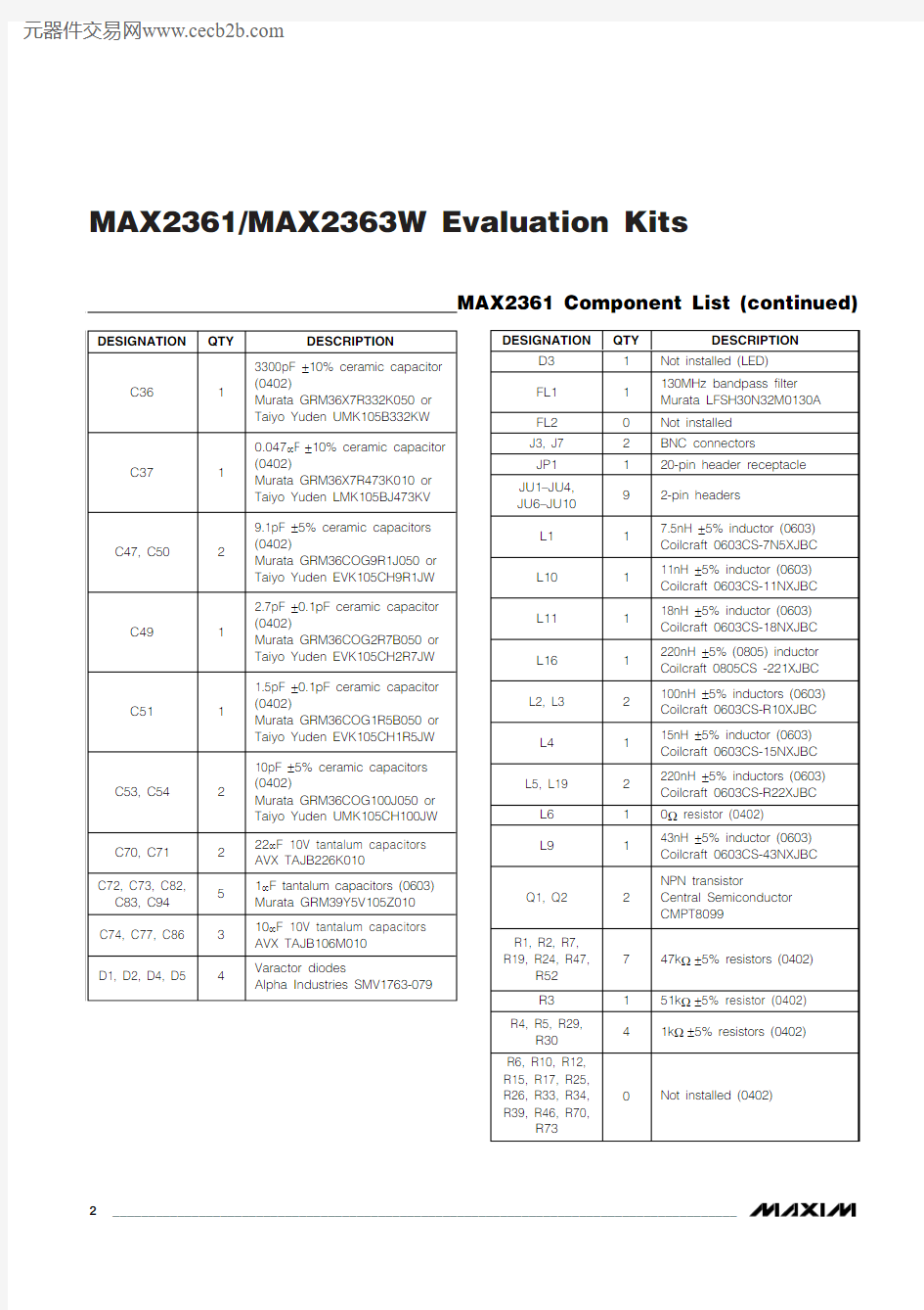
MAX2361 Component List (continued)
E v a l u a t e : M A X 2361/M A X 2363/M A X 2365
MAX2361/MAX2363W Evaluation Kits 4_______________________________________________________________________________________
Evaluate: MAX2361/MAX2363/MAX2365
MAX2361/MAX2363W Evaluation Kits
_______________________________________________________________________________________5
MAX2363W Component List (continued)
E v a l u a t e : M A X 2361/M A X 2363/M A X 2365
MAX2361/MAX2363W Evaluation Kits 6
_______________________________________________________________________________________
The MAX2361/MAX2363W EV kits are fully assembled and factory tested. Follow the instructions in the Connections and Setup section.
Test Equipment Required
This section lists the recommended test equipment to verify the operation of the MAX2361/MAX2363/MAX2365. It is intended as a guide only, and substitu-tions may be possible.
?One TCXO (Temperature-Components Crystal Oscillator) at 19.68MH z for the PLL reference fre-quency
?An RF spectrum analyzer with optional digital modu-lation personality (Rohde & Schwarz FSEA30 or equivalent)? A power supply that can provide 250mA at +3.3V ? A power supply that can provide 50mA at +5V
?An additional voltage source for control of VGA func-tions
?I/Q arbitrary waveform generator or CDMA generator
(Agilent E4433B or equivalent)
?PC (486DX33 or better) with Win95?/98?, Win2000?,WinNT ?4.0 or later operating system and an avail-able parallel port
?INTF2300 interface board (supplied with EV kit)
Connections and Setup
This section provides step-by-step instructions for get-ting the EV kit up and running in cellular and PCS CDMA modes.
Cellular CDMA Mode
Perform the following steps to evaluate the MAX2361 in the cellular CDMA mode:
1)
Verify shunts JU1, JU2, and JU6–JU10 are in place.2)Connect the INTF2300 interface cable as shown in
Figure 8. Note:Pin 1 of the interface cable corre-sponds to the red wire. Pin 1 is designated in silkscreen on each of the PC boards.
3)Connect a +3.0V power supply to VBAT. The
INTF2300 board derives its power from the MAX2361EV kit.
4)Connect a +5.0V power supply to the header labeled
“+5V ”.
5)Connect the TCXO to the REF port.
6)Connect a CDMA baseband signal generator to the
I and Q ports using BNC connectors. Set the modu-lation to reverse-channel CDMA
7)Install and run Maxim CDMA control software.
Software is also available on the web at https://www.doczj.com/doc/147035954.html, . On the IC selection form, click on the MAX236X control button. Select P4. Click on register views.
8)With the MAX236X control screen active, set the reg-isters according to Table 1.
9)Click on the Send Data button for each of the con-trol registers located at the right of the screen.There are eight registers that need to be down-loaded to the IC. The Lock indicator on the screen (and on the EV board) should be red, indicating lock.
10)Apply 2.4V to GC via JU4.
11)Connect RFL to the spectrum analyzer. Configure
the spectrum analyzer to measure ACPR for reverse-channel CDMA. Set the center frequency to 836MHz with a +10dBm reference level.
12)The output power should be about +9dBm after
accounting for cable and connector loss. The ACPR at ±885kHz offset should be -54dBc, and the ACPR at ±1.98MHz offset should be -65dBc.
MAX2363W Component List
(continued)
Win95?/98?, Win2000?, WinNT ?are registered trademarks of Microsoft Corp.
Evaluate: MAX2361/MAX2363/MAX2365
MAX2361/MAX2363W Evaluation Kits
_______________________________________________________________________________________
7
Upper Half-Band PCS CDMA Mode
Perform the following steps to evaluate the MAX2361 in the PCS CDMA mode:
1)Remove shunt JU2 and place shunt in JU3. This
removes V CC for the cellular VCO and applies V CC to the PCS VCO.
2)With the MAX236X control screen active, set the
registers according to Table 1.3)Click on the Send Data buttons for each of the con-trol registers located at the right of the screen.There are eight registers that need to be down-loaded to the IC. The lock indicator on the screen should be red, indicating lock.4)Apply a 2.4V to VGC via JU4.
5)Connect the RFH 0 port to the spectrum analyzer.
Configure the spectrum analyzer to measure ACPR for reverse-channel CDMA. Set the center frequen-cy to 1880.01MHz with a +10dBm reference level.6)The output power should be about +9dBm after
accounting for cable and connector loss. The ACPR at ±1.25MHz offset should be -54dBc.Wide-Band CDMA Mode
Perform the following steps to evaluate the MAX2363 in the wideband CDMA mode:
1)Remove shunt JU2 and place shunt in JU3. This
removes V CC for the cellular VCO and applies V CC to the WCDMA VCO.
2)Connect a TCXO at 15.36MHz to REF port.
3)Set the modulation of the baseboard signal genera-tor to 3GPP WCDMA reverse link.4)With the MAX236X control screen active, set the
registers according to Table 1.
5)Click on the Send Data buttons for each of the con-trol registers located at the right of the screen.There are eight registers that need to be down-loaded to the IC. The Lock indicator on the screen should be red, indicating lock.6)Apply a 2.4V to VGC via JU4.
7)Connect the RFH 0 port to the spectrum analyzer.
Configure the spectrum analyzer to measure ACPR for reverse-channel WCDMA. Set the center fre-quency to 1950MHz with a +10dBm reference level.8)The output power should be about +9dBm after
accounting for cable and connector loss. The ACPR at ±5MHz offset should be -44dBc.
Adjustments and Control
VGA Adjust
Apply a voltage from 0.6V to 2.4V to header “VGC ” to adjust the IF and RF VGA of the MAX2361/MAX2363/MAX2365. The VGC voltage is filtered on the EV kit to minimize undesired amplitude modulation.
Interface Control
The interface port is designed to use a 20-pin ribbon cable (Figure 1); 10 pins are signal lines, and the other 10 pins are digital grounds. Pin 1 of the interface cable is red. Pin 1 is also designated in silk screen on each of the PC boards.
Detailed Description
The following section covers the EV kits ’ circuit blocks in detail (refer to the MAX2361/MAX2363/MAX2365data sheet for additional information).
I/Q Inputs
The single-ended I/Q signals are converted to differen-tial by operational amplifiers on the EV kit. The op amps also provide DC bias to the I/Q input pins of the MAX2361/MAX2363/MAX2365. The EV kits are set up to provide 415mVp-p differential to the IC when used with a 50?source that delivers 1Vp-p into 50?. For other I/Q levels, replace R9 and R18 with appropriate resistor values according to Table 2.
Programming Interface
The programming interface is provided by the INTF2300 interface board. The interface board buffers and level shifts logic levels from the PC to the MAX2361/MAX2363W EV kits (refer to the INTF2300documentation). These logic signals control the logic pins as well as the serial interface.
IFLO
The IFLO output port provides an output signal that is either the IF VCO frequency or the VCO frequency divided by 2, depending on the setting of the BUF_DIV control bit. It can be enabled by setting the BUF_EN bit to 1 in the OPCTRL register.
TANK BYP
The tank bypass port is provided to drive the high-band tank with an external LO source. The VCO_BYPASS bit should be set to 1 to enable this port. Replace C25 with 0.01μF AC-coupling capacitor; replace R36 and R70 with 0?resistors; and remove R38, C12, C24, L10, D1, and D2.
REF
REF is the reference frequency input to the RF and IF PLL. The REF port is AC-coupled. Make sure the refer-ence signal has low phase noise.
LOH
LOH is the high-band RF LO input port. The EV kit is shipped with this port disconnected. To use this port with an external signal source, disconnect the PCS VCO by removing C39 and placing it at location C66.
LOL
LOL is the low-band RF LO input port. The EV kit is shipped with this port disconnected. To use this port with an external signal source, disconnect the cellular VCO by removing C40 and placing it at location C65.
RFH1
RFH 1 is the PCS lower half-band PA driver output.Refer to Table 9 in the MAX2361/MAX2363/MAX2365data sheet for the mode description.
RFL
RFL is the cellular band PA driver output. This port is active in cellular and FM modes. Refer to Table 9 in the MAX2361/MAX2363/MAX2365 data sheet for the mode description.
RFH0
RFH 0 is the PCS upper half-band PA driver output.Refer to Table 9 in the MAX2361/MAX2363/MAX2365data sheet for the mode description.
IFINH and IFOUTH
For cascade evaluation, an on-board filter is connected between IFOUTH and IFINH. Select these ports by pro-gramming IF_SEL to 1. IFINH and IFOUTH are not con-nected to SMA connectors on the EV kit
IFINL and IFOUTL
For cascade evaluation, an on-board filter is connected between IFOUTL and IFINL. Select these ports by pro-gramming IF_SEL to 0. For individual IF modulator and upconverter evaluation, remove R44, R49, R55, R58,and install R25, R33, R34, and R39 with 0?resistors.This connects the IFINL_ and IFOUTL_ pins to the IFINL and IFOUTL SMA connectors. The matching networks are tuned to 130MHz.
VBAT/VREG
VBAT supplies V CC to the PA driver circuitry. This may be an unregulated battery voltage. The PA drivers are open collector. Jumpers are provided to enable current mea-surement to each functional block of the IC (Table 3).
VREG is connected to the output of the U2 regulator on the EV Kit. Do not connect an external supply voltage to VREG header.
RBIAS
When resistor R73 is stuffed (typically 10k ?), a bias volt-age may be applied to the RBIAS header to adjust the PA driver bias current. Internal to the IC, pin 12 is set to 600mV. Output linearity or efficiency may be improved by adjusting PA driver current.
Layout Considerations
The MAX2361/MAX2363W EV kits can serve as guides for your board layout. Keep PC board trace lengths as
E v a l u a t e : M A X 2361/M A X 2363/M A X 2365
MAX2361/MAX2363W Evaluation Kits 8
short as possible to minimize parasitics. Also, keep decoupling capacitors as close to the IC as possible with a direct connection to the ground plane.
PC Board Construction The MAX2361/MAX2363W EV kit PC board uses a 14mil-wide trace for 50?transmission line. The PC board has an 8mil-layer profile on FR4 with a dielectric constant of 4.5.
INTF2300 SPI Interface Board
The INTF2300 interface board is used to interface
3-wire SPI protocol from a PC’s parallel port to the EV
kit. This board will level translate 5V logic from the PC
to V CC of the EV kit (typically this will be 3.3V logic).
The INTF2300 also provides buffering and EMI filtering.
Its absolute maximum supply voltage is 4.6V, limited by
the breakdown of the buffer IC. The recommended operating supply voltage range is +2.7V to +3.6V. Evaluate: MAX2361/MAX2363/MAX2365
MAX2361/MAX2363W Evaluation Kits
_______________________________________________________________________________________9 Figure 1. INTF2300 with MAX2361/MAX2363W EV Kit Providing Filtered Supply
E v a l u a t e : M A X 2361/M A X 2363/M A X 2365
MAX2361/MAX2363W Evaluation Kits 10
______________________________________________________________________________________
Figure 2. MAX2361/MAX2363W EV Kit Schematic
Evaluate: MAX2361/MAX2363/MAX2365
MAX2361/MAX2363W Evaluation Kits
______________________________________________________________________________________
11
Figure 2. MAX2361/MAX2363W EV Kit Schematic (continued)
E v a l u a t e : M A X 2361/M A X 2363/M A X 2365
MAX2361/MAX2363W Evaluation Kits 12______________________________________________________________________________________
Figure 3. MAX2361/MAX2363W EV Kit Component Placement
Guide—Component Side (Top View)Figure 4. MAX2361/MAX2363W EV Kit Component Placement
Guide—Solder Side (Bottom View)
Figure 5. MAX2361/MAX2363W EV Kit PC Board Layout—
Component Side (Top View)Figure 6. MAX2361/MAX2363W EV Kit PC Board Layout—
Ground Plane (Top View)
MAX2361/MAX2363W Evaluation Kits Maxim cannot assume responsibility for use of any circuitry other than circuitry entirely embodied in a Maxim product. No circuit patent licenses are
implied. Maxim reserves the right to change the circuitry and specifications without notice at any time.
Maxim Integrated Products, 120 San Gabriel Drive, Sunnyvale, CA 94086 408-737-7600 ____________________13
?2001 Maxim Integrated Products Printed USA
is a registered trademark of Maxim Integrated Products.
Figure 7. MAX2361/MAX2363W EV Kit PC Board Layout—Inner
Layer (Top View)Figure 8. MAX2361/MAX2363W EV Kit PC Board Layout—
Solder Side (Bottom View)
Evaluate: MAX2361/MAX2363/MAX2365