
RF Power Field Effect Transistors
N-Channel Enhancement-Mode Lateral MOSFETs
Designed for GSM and GSM EDGE base station applications with frequencies from 869 to 960 MHz. Suitable for multicarrier amplifier applications.
GSM Application
?Typical GSM Performance: V DD = 26 Volts, I DQ = 700 mA, P out =
100 Watts CW, Full Frequency Band (869-894 MHz and 921-960 MHz)Power Gain - 17.5 dB Drain Efficiency - 60%GSM EDGE Application
?Typical GSM EDGE Performance: V DD = 28 Volts, I DQ = 650 mA, P out = 50 Watts Avg., Full Frequency Band (869-894 MHz and 921-960 MHz)Power Gain — 18 dB
Spectral Regrowth @ 400 kHz Offset = -63 dBc Spectral Regrowth @ 600 kHz Offset = -78 dBc EVM — 2.3% rms
?Capable of Handling 10:1 VSWR, @ 26 Vdc, @ 100 W CW Output Power, @ f = 960 MHz
?Characterized with Series Equivalent Large-Signal Impedance Parameters ?Internally Matched for Ease of Use
?Qualified Up to a Maximum of 32 V DD Operation ?Integrated ESD Protection
?N Suffix Indicates Lead-Free Terminations ?200°C Capable Plastic Package
?In Tape and Reel. R1 Suffix = 500 Units per 44 mm, 13 inch Reel.
Table 1. Maximum Ratings
Rating
Symbol Value Unit Drain-Source Voltage V DSS -0.5, +68Vdc Gate-Source Voltage
V GS -0.5, +15Vdc Total Device Dissipation @ T C = 25°C Derate above 25°C P D 4272.44W W/°C Storage Temperature Range T stg -65 to +150
°C Operating Junction Temperature
T J
200
°C
Table 2. Thermal Characteristics
Characteristic
Symbol Value (1,2)
Unit Thermal Resistance, Junction to Case Case Temperature 80°C, 100 W CW Case Temperature 80°C, 50 W CW
R θJC
0.410.47
°C/W
1.MTTF calculator available at https://www.doczj.com/doc/124438819.html,/rf. Select Tools/Software/Application Software/Calculators to access the MTTF calculators by product.
2.Refer to AN1955, Thermal Measurement Methodology of RF Power Amplifiers. Go to https://www.doczj.com/doc/124438819.html,/rf. Select Documentation/Application Notes - AN1955.Document Number: MRF5S9101
Rev. 2, 7/2005
Freescale Semiconductor Technical Data
MRF5S9101NR1MRF5S9101NBR1MRF5S9101MR1MRF5S9101MBR1
2
RF Device Data
Freescale Semiconductor
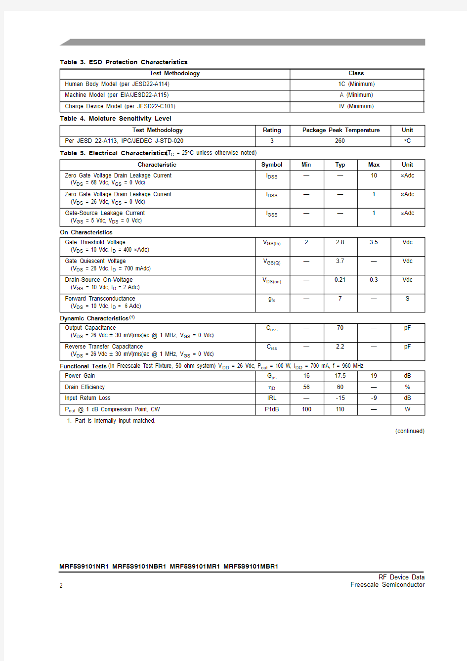
MRF5S9101NR1 MRF5S9101NBR1 MRF5S9101MR1 MRF5S9101MBR1Table 3. ESD Protection Characteristics
Test Methodology
Class Human Body Model (per JESD22-A114)1C (Minimum)Machine Model (per EIA/JESD22-A115) A (Minimum)Charge Device Model (per JESD22-C101)
IV (Minimum)
Table 4. Moisture Sensitivity Level
Test Methodology
Rating Package Peak Temperature
Unit Per JESD 22-A113, IPC/JEDEC J-STD-020
3
260
°C
Table 5. Electrical Characteristics (T C = 25°C unless otherwise noted)
Characteristic
Symbol Min Typ Max Unit Zero Gate Voltage Drain Leakage Current (V DS = 68 Vdc, V GS = 0 Vdc)
I DSS ——10μAdc Zero Gate Voltage Drain Leakage Current (V DS = 26 Vdc, V GS = 0 Vdc)I DSS ——1μAdc Gate-Source Leakage Current (V GS = 5 Vdc, V DS = 0 Vdc)I GSS
—
—
1
μAdc
On Characteristics
Gate Threshold Voltage
(V DS = 10 Vdc, I D = 400 μAdc)V GS(th)2 2.8 3.5Vdc Gate Quiescent Voltage
(V DS = 26 Vdc, I D = 700 mAdc)V GS(Q)— 3.7—Vdc Drain-Source On-Voltage (V GS = 10 Vdc, I D = 2 Adc)V DS(on)—0.210.3Vdc Forward Transconductance (V DS = 10 Vdc, I D = 6 Adc)g fs
—
7
—
S
Dynamic Characteristics (1)
Output Capacitance
(V DS = 26 Vdc ± 30 mV(rms)ac @ 1 MHz, V GS = 0 Vdc)C oss —70—pF Reverse Transfer Capacitance
(V DS = 26 Vdc ± 30 mV(rms)ac @ 1 MHz, V GS = 0 Vdc)C rss
—
2.2
—
pF
Functional Tests (In Freescale Test Fixture, 50 ohm system) V DD = 26 Vdc, P out = 100 W, I DQ = 700 mA, f = 960 MHz
Power Gain G ps 1617.519dB Drain Efficiency ηD 5660—%Input Return Loss
IRL —-15-9dB P out @ 1 dB Compression Point, CW P1dB
100
110
—
W
1.Part is internally input matched.
(continued)
MRF5S9101NR1 MRF5S9101NBR1 MRF5S9101MR1 MRF5S9101MBR1
3
RF Device Data
Freescale Semiconductor
Table 5. Electrical Characteristics (T C = 25°C unless otherwise noted) (continued)
Characteristic
Symbol
Min
Typ
Max
Unit
Typical GSM EDGE Performances (In Freescale GSM EDGE Test Fixture, 50 οhm system) V DD = 28 Vdc, P out = 50 W Avg., I DQ = 650 mA, 869 MHz EVM — 2.3—% rms Spectral Regrowth at 400 kHz Offset SR1—-63—dBc Spectral Regrowth at 600 kHz Offset SR2 — -78 — dBc 4 RF Device Data Freescale Semiconductor MRF5S9101NR1 MRF5S9101NBR1 MRF5S9101MR1 MRF5S9101MBR1Z10.698″ x 0.827″ Microstrip Z20.720″ x 0.788″ Microstrip Z30.195″ x 0.087″Microstrip Z40.524″ x 0.087″Microstrip Z50.233″ x 0.087″Microstrip Z60.560″ x 0.087″ Microstrip Z70.095″ x 0.827″ Microstrip Z80.472″ x 0.087″ Microstrip Z90.384″ x 0.087″ Microstrip Z10 1.491″ x 0.087″ Microstrip Z11, Z12* 1.6″ x 0.089″ Microstrip (quarter wave length for supply purpose)Z13* 1.2″ x 0.059″ Microstrip (quarter wave length for bias purpose)PCB Taconic TLX8-0300, 0.030″, εr = 2.55 *Variable for tuning Figure 1. MRF5S9101NR1(NBR1)/MR1(MBR1) 900 MHz Test Circuit Schematic V Table 6. MRF5S9101NR1(NBR1)/MR1(MBR1) 900 MHz Test Circuit Component Designations and Values Part Description Part Number Manufacturer C1, C2, C3 4.7 m F Chip Capacitors (2220)GRM55ER7H475KA01Murata C4, C5, C610 nF 200B Chip Capacitors 200B103MW ATC C7, C8, C933 pF 100B Chip Capacitors 100B330JW ATC C10, C1122 pF 100B Chip Capacitors 100B220GW ATC C12, C13 10 pF 100B Chip Capacitors 100B100GW ATC C14, C15, C16, C178.2 pF 100B Chip Capacitors 100B8R2CW ATC C18 5.6 pF 100B Chip Capacitor 100B5R6CW ATC C19 4.7 pF 100B Chip Capacitor 100B4R7BW ATC C20 3.9 pF 100B Chip Capacitor 100B3R9BW ATC C21220 m F, 50 V Electrolytic Capacitor, Axial 516D227M050NP7B Sprague R1, R210 k W , 1/4 W Chip Resistors (1206)R3 10 W , 1/4 W Chip Resistor (1206) MRF5S9101NR1 MRF5S9101NBR1 MRF5S9101MR1 MRF5S9101MBR1 5 RF Device Data Freescale Semiconductor Figure 2. MRF5S9101NR1(NBR1)/MR1(MBR1) 900 MHz Test Circuit Component Layout Freescale has begun the transition of marking Printed Circuit Boards (PCBs) with the Freescale Semiconductor signature/logo. PCBs may have either Motorola or Freescale markings during the transition period. These changes will have no impact on form, fit or function of the current product. 6 RF Device Data Freescale Semiconductor MRF5S9101NR1 MRF5S9101NBR1 MRF5S9101MR1 MRF5S9101MBR1TYPICAL CHARACTERISTICS - 900 MHz 1020 1018860 ?4570 601750164015301401312?1511?30880 900 920 940 960 980 1000 G p s , P O W E R G A I N (d B ) I N P U T R E T U R N L O S S (d B )I R L ,f, FREQUENCY (MHz) Figure 3. Power Gain, Input Return Loss and Drain Efficiency versus Frequency @ P out = 100 Watts CW 1020 1019860 ?245045173516301514?81312?1611?20880 900 920 940 960 980 1000 G p s , P O W E R G A I N (d B ) f, FREQUENCY (MHz) Figure 4. Power Gain, Input Return Loss and Drain Efficiency versus Frequency @ P out = 40 Watts CW 18?12401000 14191 P out , OUTPUT POWER (WATTS)Figure 5. Power Gain versus Output Power G p s , P O W E R G A I N (d B ) 1817 16 15 10 100200 P out , OUTPUT POWER (WATTS) CW Figure 6. Power Gain versus Output Power 20 40 60 80 100 120 140 160 180 ηD , D R A I N E F F I C I E N C Y (%)I N P U T R E T U R N L O S S (d B )I R L ,ηD , D R A I N E F F I C I E N C Y (%) MRF5S9101NR1 MRF5S9101NBR1 MRF5S9101MR1 MRF5S9101MBR1 7 RF Device Data Freescale Semiconductor TYPICAL CHARACTERISTICS - 900 MHz G p s , P O W E R G A I N (d B ) 1320 1918 17161514 100 1 P out , OUTPUT POWER (WATTS) AVG. Figure 9. Error Vector Magnitude and Drain Efficiency versus Output Power 10 980 ?83?63 900 f, FREQUENCY (MHz) Figure 10. Spectral Regrowth at 400 kHz and 600 kHz versus Frequency S P E C T R A L R E G R O W T H @ 400 k H z a n d 600 k H z (d B c ) ?68 ?73 ?78 910 920 930 940 950 960 970 90 ?80 ?450 P out , OUTPUT POWER (WATTS) AVG. Figure 11. Spectral Regrowth at 400 kHz versus Output Power S P E C T R A L R E G R O W T H @ 400 k H z (d B c ) ?60?65?7010 20 30 40 50 60 70 80 ?50?55 ?75 8 RF Device Data Freescale Semiconductor MRF5S9101NR1 MRF5S9101NBR1 MRF5S9101MR1 MRF5S9101MBR1TYPICAL CHARACTERISTICS - 900 MHz 90 ?85?650 P out , OUTPUT POWER (WATTS) AVG. Figure 12. Spectral Regrowth @ 600 kHz versus Output Power S P E C T R A L R E G R O W T H @ 600 k H z (d B c ) ?70 ?75 ?80 10 20 30 40 50 60 70 80 T J , JUNCTION TEMPERATURE (°C) This above graph displays calculated MTTF in hours x ampere 2drain current. Life tests at elevated temperatures have correlated to better than ±10% of the theoretical prediction for metal failure. Divide MTTF factor by I D 2 for MTTF in a particular application. Figure 13. MTTF Factor versus Junction Temperature 210 1.E+07 1.E+1090 M T T F F A C T O R (H O U R S X A M P S 2) 1.E+09 1.E+08 100110120130140150160170180190200 MRF5S9101NR1 MRF5S9101NBR1 MRF5S9101MR1 MRF5S9101MBR1 9 RF Device Data Freescale Semiconductor Figure 14. MRF5S9101NR1(NBR1)/MR1(MBR1) 800 MHz Test Circuit Schematic Z10.432″ x 0.827″ Microstrip Z20.720″ x 0.788″ Microstrip Z30.195″ x 0.087″ Microstrip Z40.584″ x 0.087″ Microstrip Z50.173″ x 0.087″ Microstrip Z60.560″ x 0.087″ Microstrip Z70.378″ x 0.827″ Microstrip Z80.279″ x 0.087″ Microstrip Z90.193″ x 0.087″ Microstrip Z100.897″ x 0.087″ Microstrip Z11 1.161″ x 0.087″ Microstrip Z12, Z13* 1.6″ x 0.089″ Microstrip (quarter wave length for supply purpose)Z14* 1.2″ x 0.059″ Microstrip (quarter wave length for bias purpose)PCB Taconic TLX8-0300, 0.030″, εr = 2.55 *Variable for tuning V Table 7. MRF5S9101NR1(NBR1)/MR1(MBR1) 800 MHz Test Circuit Component Designations and Values Part Description Part Number Manufacturer C1, C2, C3 4.7 m F Chip Capacitors (2220)GRM55ER7H475KA01Murata C4, C5, C610 nF 200B Chip Capacitors 200B103MW ATC C7, C8, C933 pF 100B Chip Capacitors 100B330JW ATC C10, C1122 pF 100B Chip Capacitors 100B220GW ATC C12, C13, C1710 pF 100B Chip Capacitors 100B100GW ATC C14, C158.2 pF 100B Chip Capacitors 100B8R2CW ATC C16, C22 6.8 pF 100B Chip Capacitors 100B6R8CW ATC C18 5.6 pF 100B Chip Capacitor 100B5R6CW ATC C19, C20 2.7 pF 100B Chip Capacitors 100B2R7BW ATC C21220 m F, 50 V Electrolytic Capacitor, Axial 516D227M050NP7B Sprague R1, R210 k W , 1/4 W Chip Resistors (1206)R3 10 W , 1/4 W Chip Resistor (1206) 10 RF Device Data Freescale Semiconductor MRF5S9101NR1 MRF5S9101NBR1 MRF5S9101MR1 MRF5S9101MBR1Figure 15. MRF5S9101NR1(NBR1)/MR1(MBR1) 800 MHz Test Circuit Component Layout Freescale has begun the transition of marking Printed Circuit Boards (PCBs) with the Freescale Semiconductor signature/logo. PCBs may have either Motorola or Freescale markings during the transition period. These changes will have no impact on form, fit or function of the current product. MRF5S9101NR1 MRF5S9101NBR1 MRF5S9101MR1 MRF5S9101MBR1 11 RF Device Data Freescale Semiconductor TYPICAL CHARACTERISTICS - 800 MHz 940 1020820?2065 196018551750164515?1014?1213?1412?1611 ?18 830840850860870880890900910920930f, FREQUENCY (MHz) Figure 16. Power Gain, Input Return Loss and Drain Efficiency versus Frequency @ P out = 100 W CW G p s , P O W E R G A I N (d B ) 940 1020820?2045 f, FREQUENCY (MHz) Figure 17. Power Gain, Input Return Loss and Drain Efficiency versus Frequency @ P out = 40 W CW G p s , P O W E R G A I N (d B ) 194018351730162515?1014?1213?1412?1611 ?18 830840850860870880890900910920930910 03.5850 f, FREQUENCY (MHz) Figure 18. Error Vector Magnitude versus Frequency E V M , E R R O R V E C T O R M A G N I T U D E (% r m s ) 32.521.510.5860 870 880 890 900 100 1 60P out , OUTPUT POWER (WATTS) AVG. Figure 19. Error Vector Magnitude and Drain Efficiency versus Output Power , D R A I N E F F I C I E N C Y (%) η50403020 1010 I N P U T R E T U R N L O S S (d B )I R L ,ηD , D R A I N E F F I C I E N C Y (%)I N P U T R E T U R N L O S S (d B )I R L ,ηD , D R A I N E F F I C I E N C Y (%) 12 RF Device Data Freescale Semiconductor MRF5S9101NR1 MRF5S9101NBR1 MRF5S9101MR1 MRF5S9101MBR1TYPICAL CHARACTERISTICS - 800 MHz 910 ?82?64850 f, FREQUENCY (MHz) Figure 20. Spectral Regrowth at 400 kHz and 600 kHz versus Frequency S P E C T R A L R E G R O W T H @ 400 k H z A N D 600 k H z (d B c ) ?66?68?70?72 ?74?76?78?80860 870 880 900 890 90 ?80?450 P out , OUTPUT POWER (WATTS) AVG. Figure 21. Spectral Regrowth at 400 kHz versus Output Power S P E C T R A L R E G R O W T H @ 400 k H z (d B c ) 10 20 30 40 50 60 70 80 ?50?55?60?65?70?7590 ?85?650 P out , OUTPUT POWER (WATTS) AVG. Figure 22. Spectral Regrowth at 600 kHz versus Output Power S P E C T R A L R E G R O W T H @ 400 k H z (d B c ) ?70 ?75 ?80 10 20 30 40 50 60 70 80 MRF5S9101NR1 MRF5S9101NBR1 MRF5S9101MR1 MRF5S9101MBR1 13 RF Device Data Freescale Semiconductor Figure 23. Series Equivalent Source and Load Impedance f MHz Z source ?Z load ?845865 4.29 - j2.232.72 - j0.963.94 - j1.24 1.15 - j0.041.05 - j0.101.02 - j0.07V DD = 26 Vdc, I DQ = 700 mA, P out = 100 W CW Z o = 5 ? f = 990 MHz f = 990 MHz f = 845 MHz f = 845 MHz 890920 1.96 - j1.02 1.03 - j0.15Z load Z source Z source =Test circuit impedance as measured from gate to ground.Z load =Test circuit impedance as measured from drain to ground. Z source Z load Output Matching Network 1.58 - j1.43 1.03 - j0.05960990 1.27 - j1.54 0.73 - j0.07 14 RF Device Data Freescale Semiconductor MRF5S9101NR1 MRF5S9101NBR1 MRF5S9101MR1 MRF5S9101MBR1PACKAGE DIMENSIONS BOTTOM VIEW PLASTIC MRF5S9101NR1(MR1) MRF5S9101NR1 MRF5S9101NBR1 MRF5S9101MR1 MRF5S9101MBR1 15 RF Device Data Freescale Semiconductor PLASTIC MRF5S9101NBR1(MBR1) https://www.doczj.com/doc/124438819.html,
相关主题
文本预览