Properties of amorphous Si-rich silicon nitride prepared by rf-magnetron sputtering
- 格式:pdf
- 大小:141.52 KB
- 文档页数:6
廖乃镘:男,1979年生,博士研究生,从事氢化非晶硅红外敏感薄膜材料研究 Tel :028********* E 2mail :liaonaiman @ 李伟:通讯联系人,教授,博士生导师 Tel :028********* E 2mail :wli @氢化非晶硅(a 2Si ∶H )薄膜稳定性的研究进展廖乃镘,李 伟,蒋亚东,匡跃军,李世彬,吴志明(电子科技大学电子薄膜与集成器件国家重点实验室,成都610054) 摘要 氢化非晶硅(a 2Si ∶H )是一种重要的光敏感薄膜材料,其稳定性的好坏是决定能否应用于器件的重要因素之一。
介绍了a 2Si ∶H 薄膜稳定性的研究进展,论述了a 2Si ∶H 薄膜的稳定性与Si 2Si 弱键的关系,分析了光致衰退效应(S 2W 效应)产生的几种机理,提出了在薄膜制备和后处理过程中消除或减少Si 2Si 弱键以提高a 2Si ∶H 薄膜稳定性的方法。
关键词 氢化非晶硅 稳定性 光致衰退效应 物理模型 稳定化处理R ecent Progresses on the Stability of H ydrogenated Amorphous Silicon Thin FilmsL IAO Naiman ,L I Wei ,J IAN G Yadong ,KUAN G Yuejun ,L I Shibin ,WU Zhiming(State Key Laboratory of Electronic Thin Films and Integrated Devices ,U ESTC ,Chengdu 610054)Abstract The a 2Si ∶H thin film is an important light 2sensitive material that has received significant attentionnowadays because of its unique properties.The stability of this thin film is a key factor which is fatal in the application of commercial devices.This paper summarizes and commends some researches on the stability of a 2Si ∶H thin films based on recent literature ,and discusses the relationship between the weak bonding of Si 2Si and the stability of the films.It introduces the mechanisms of light 2induced degeneration of a 2Si ∶H thin films and also recommends some methods of film fabrication and post 2treatment techniques in order to reduce the weak bonding of Si 2Si in a 2Si ∶H thin films.K ey w ords a 2Si ∶H ,stability ,light 2induced degeneration ,physical model ,stabilization treatment 0 前言氢化非晶硅(a 2Si ∶H )薄膜具有光吸收率高、电阻温度系数(TCR )相对较大(1.8~8%/K )[1]、禁带宽度可控、可大面积低温(<400℃)成膜、基片种类不限、生产工艺较简单、与硅半导体工艺兼容等突出优点,在红外成像、太阳能电池、液晶显示、复印机感光鼓等领域得到快速发展。
a-Si Aamorphous silicon以材料結構而言,amorphous的意思是指未結晶的狀態。
Amorphous silicon膜具更作為半導體材料之特性,可用plasma CVD裝置在400℃以下的温度下形成。
因此成為使用玻璃基板之主動矩陣(active matrix)方式液晶面板的TFT主力元件材料。
Amorphous means lacking distinct crystalline in material structure’s t erm. Amorphous silicon film has the quality that can be used as material of semiconductor. It can be formed by using plasma CVD equipment under temperature of 400 degree C. Therefore, it is the major material for manufacturing TFT of LCD panel, which uses glass substrate with active matrix.a-Si TFTamorphous Silicon Thin Film Transistor以amorphous silicon為構成材料之電場效果型的薄膜電晶體。
帶更source、drain、gate三種電極之3端子元件。
最常使用為主動矩陣(active matrix)液晶顯示器的開關。
The Field Effect type TFT with amorphous silicon material contains three terminal components of three types of electrodes: source, drain, and gate. They are often used as the switch of active matrix type LCD.ACFAnisotropic Conductive Film異方性導電膜,指含更導電性粒子之熱硬化或熱可塑性的樹脂薄膜。
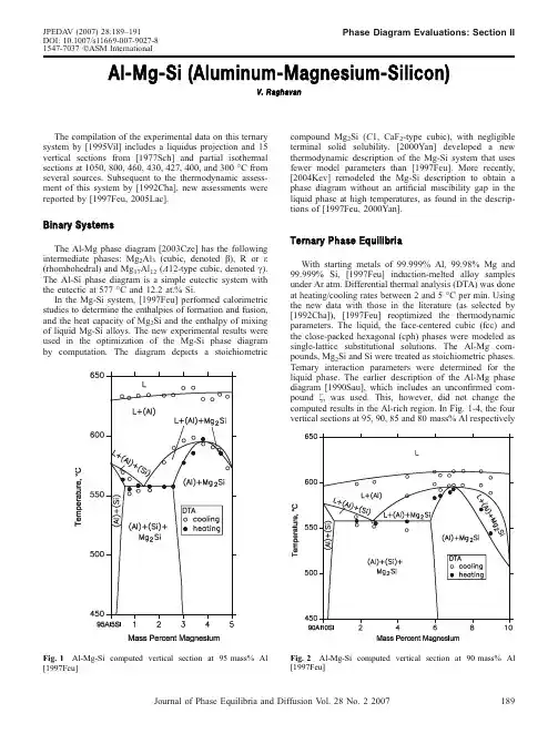
Al-Mg-Si (Aluminum-Magnesium-Silicon)V.RaghavanThe compilation of the experimental data on this ternary system by [1995Vil]includes a liquidus projection and 15vertical sections from [1977Sch]and partial isothermal sections at 1050,800,460,430,427,400,and 300°C from several sources.Subsequent to the thermodynamic assess-ment of this system by [1992Cha],new assessments were reported by [1997Feu,2005Lac].Binary SystemsThe Al-Mg phase diagram [2003Cze]has the following intermediate phases:Mg 2Al 3(cubic,denoted b ),R or e (rhombohedral)and Mg 17Al 12(A 12-type cubic,denoted c ).The Al-Si phase diagram is a simple eutectic system with the eutectic at 577°C and 12.2at.%Si.In the Mg-Si system,[1997Feu]performed calorimetric studies to determine the enthalpies of formation and fusion,and the heat capacity of Mg 2Si and the enthalpy of mixing of liquid Mg-Si alloys.The new experimental results were used in the optimization of the Mg-Si phase diagram by computation.The diagram depicts a stoichiometriccompound Mg 2Si (C 1,CaF 2-type cubic),with negligible terminal solid solubility.[2000Yan]developed a new thermodynamic description of the Mg-Si system that uses fewer model parameters than [1997Feu].More recently,[2004Kev]remodeled the Mg-Si description to obtain a phase diagram without an artificial miscibility gap in the liquid phase at high temperatures,as found in the descrip-tions of [1997Feu,2000Yan].Ternary Phase EquilibriaWith starting metals of 99.999%Al,99.98%Mg and 99.999%Si,[1997Feu]induction-melted alloy samples under Ar atm.Differential thermal analysis (DTA)was done at heating/cooling rates between 2and 5°C per ing the new data with those in the literature (as selected by [1992Cha]),[1997Feu]reoptimized the thermodynamic parameters.The liquid,the face-centered cubic (fcc)and the close-packed hexagonal (cph)phases were modeled as single-lattice substitutional solutions.The Al-Mg com-pounds,Mg 2Si and Si were treated as stoichiometric phases.Ternary interaction parameters were determined for the liquid phase.The earlier description of the Al-Mg phase diagram [1990Sau],which includes an unconfirmed com-pound f ,was used.This,however,did not change the computed results in the Al-rich region.In Fig.1-4,the four vertical sections at 95,90,85and 80mass%AlrespectivelyFig.1Al-Mg-Si computed vertical section at 95mass%Al[1997Feu]Fig.2Al-Mg-Si computed vertical section at 90mass%Al [1997Feu]JPEDAV (2007)28:189–191DOI:10.1007/s11669-007-9027-81547-7037ÓASM InternationalPhase Diagram Evaluations:Section IIJournal of Phase Equilibria and Diffusion V ol.28No.22007189computed by [1997Feu]are compared with their own DTA data on solidification temperatures.The agreement with the experimental data is good.[2005Lac]carried out a new thermodynamic assessment of this system,which uses the revised Al-Mg description with only the three intermediate phases,Mg 2Al 3(b ),e and c .They used a larger set of data for the liquid-solid equilibria from the experimental results of [1977Sch,1997Feu].Temperature-independent ternary interaction parameters were obtained for the liquid phase.A partial liquidus projection and three vertical sections at 5and 85mass%Al and 2mass%Si respectively were computed by [2005Lac].The vertical section at 2mass%Si is redrawn in Fig.5.The agreement with the experimental results of [1977Sch,1931Los]is satisfactory.The eutectic maximum (e 3)of the reaction L $ðAl ÞþMg 2Si does not lie on the Al-Mg 2Si join but on the Mg-rich side of this line [1992Cha,1997Feu,2001Bar,2005Lac].The partial liquidus projection in Fig.6depicts the above univariant line determined by [2001Bar].Other recent references on the phase equilibria of this system include [1999Esk,2002Fro,2003Erm,2003Roo,2004Liu,2005Don].References1931Los:L.Losana,The Aluminum-Magnesium-Silicon Ternary System,Metall.Italiana ,1931,23,p 367-382,in Italian1977Sch:E.Schurmann and A.Fischer,Melting Equilibria in the Ternary System Al-Mg-Si,Giessereiforschung ,1977,29(4),p 161-165,inGermanFig.3Al-Mg-Si computed vertical section at 85mass%Al[1997Feu]Fig.4Al-Mg-Si computed vertical section at 80mass%Al[1997Feu]Fig.5Al-Mg-Si computed vertical section at 2mass%Si[2005Lac]Fig.6Al-Mg-Si partial liquidus projection depicting the uni-variant line of L $ðAl ÞþMg 2Si [2001Bar]Section II:Phase Diagram Evaluations190Journal of Phase Equilibria and Diffusion V ol.28No.220071990Sau:N.Saunders,A Review and Thermodynamic assess-ment of the Al-Mg and Mg-Si Systems,CALPHAD,1990, 14(1),p61-701992Cha:N.Chakraborti and H.L.Lukas,Thermodynamic Optimization of the Mg-Al-Si Phase Diagram,CALPHAD, 1992,16(1),p79-861995Vil:P.Villars, A.Prince and H.Okamoto,Al-Mg-Si, Handbook of Ternary Alloy Phase Diagrams,vol4,ASM International,Materials Park,OH,19951997Feu:H.Feufel,T.Godecke,H.L.Lukas,and F.Sommer, Investigation of the Al-Mg-Si System by Experiments and Thermodynamic Calculations,J.Alloys Compd.,1997,247, p31-421999Esk:D.G.Eskin, A.Massardier,and P.Merle,A Study of High Temperature Precipitation of Al-Mg-Si Alloys with an Excess of Silicon,J.Mater.Sci.,1999,34(4), p811-8202000Yan:X.Y.Yan,F.Zhang,and Y.A.Chang,A Thermody-namic Analysis of the Mg-Si System,J,Phase Equilibria,2000, 21(4),p379-3842001Bar:O.M.Barabash,O.V.Sulgenko,T.N.Legkaya,and N.P. Korzhova,Experimental Analysis and Thermodynamic Calcu-lation of the Structural Regularities in the Fusion Diagram of the System of Alloys Al-Mg-Si,J.Phase Equilibria,2001, 22(1),p5-112002Fro:A.G.Froseth,S.J.Andersen, C.D.Marioara,P.M. Derlet,and R.Hoier,Solving the Structure of Phases in theAl-Mg-Si Alloy System with the Help of ab initio Modeling, Mater.Res.Soc.Symp.Proc.,2002,755,p19-242003Cze:T.Czeppe,W.Zakulski,and E.Bielanska,Study of the Thermal Stability of Phases in the Mg-Al System,J.Phase Equilibria,2003,24(3),p249-2542003Erm:S.V.Ermakova,K.D.Savelev,and V.M.Golod, Thermodynamic Study of Equilibrium Solidification and Ther-mophysical Properties of Al-Si-Mg System Alloys,Liteinoe Proizvodstvo,2003,9(Suppl.),p9-12,in Russian2003Roo:A.Roosz,J.Farkas,and G.Kaptay,Thermodynamics Based Semi-empirical Description of the Liquidus Surface and Partition Coefficients in Ternary Al-Mg-Si Alloy,Mater.Sci. Forum,2003,414-415,p323-3282004Kev:D.Kevorkov,R.Schmid-Fetzer,and F.Zhang,Phase Equilibria and Thermodynamics of the Mg-Si-Li System and Remodeling of the Mg-Si System,J.Phase Equilib.Diffus., 2004,25(2),p140-1512004Liu:Y.Q.Liu,A.Das,and Z.Fan,Thermodynamic Predic-tions of Mg-Al-M(M=Zn,Mn,Si)Alloy Compositions Amenable to Semisolid Metal Processing,Mater.Sci.Technol., 2004,20(1),p35-412005Don:H.B.Dong and R.Brooks,Determination of Liquidus Temperature in Al-Si and Al-Si-Mg Alloys Using a Single-Pan Scanning Calorimeter,Mater.Sci.Eng.A,2005,A413-A414, p480-4842005Lac:caze and R.Valdes,CALPHAD-type Assessment of the Al-Mg-Si System,Monatsh Chem.,2005,136(11),p1899-1907 Phase Diagram Evaluations:Section IIJournal of Phase Equilibria and Diffusion V ol.28No.22007191。
Modeling of morphology evolution in the injection moldingprocess of thermoplastic polymersR.Pantani,I.Coccorullo,V.Speranza,G.Titomanlio* Department of Chemical and Food Engineering,University of Salerno,via Ponte don Melillo,I-84084Fisciano(Salerno),Italy Received13May2005;received in revised form30August2005;accepted12September2005AbstractA thorough analysis of the effect of operative conditions of injection molding process on the morphology distribution inside the obtained moldings is performed,with particular reference to semi-crystalline polymers.The paper is divided into two parts:in the first part,the state of the art on the subject is outlined and discussed;in the second part,an example of the characterization required for a satisfactorily understanding and description of the phenomena is presented,starting from material characterization,passing through the monitoring of the process cycle and arriving to a deep analysis of morphology distribution inside the moldings.In particular,fully characterized injection molding tests are presented using an isotactic polypropylene,previously carefully characterized as far as most of properties of interest.The effects of both injectionflow rate and mold temperature are analyzed.The resulting moldings morphology(in terms of distribution of crystallinity degree,molecular orientation and crystals structure and dimensions)are analyzed by adopting different experimental techniques(optical,electronic and atomic force microscopy,IR and WAXS analysis).Final morphological characteristics of the samples are compared with the predictions of a simulation code developed at University of Salerno for the simulation of the injection molding process.q2005Elsevier Ltd.All rights reserved.Keywords:Injection molding;Crystallization kinetics;Morphology;Modeling;Isotactic polypropyleneContents1.Introduction (1186)1.1.Morphology distribution in injection molded iPP parts:state of the art (1189)1.1.1.Modeling of the injection molding process (1190)1.1.2.Modeling of the crystallization kinetics (1190)1.1.3.Modeling of the morphology evolution (1191)1.1.4.Modeling of the effect of crystallinity on rheology (1192)1.1.5.Modeling of the molecular orientation (1193)1.1.6.Modeling of theflow-induced crystallization (1195)ments on the state of the art (1197)2.Material and characterization (1198)2.1.PVT description (1198)*Corresponding author.Tel.:C39089964152;fax:C39089964057.E-mail address:gtitomanlio@unisa.it(G.Titomanlio).2.2.Quiescent crystallization kinetics (1198)2.3.Viscosity (1199)2.4.Viscoelastic behavior (1200)3.Injection molding tests and analysis of the moldings (1200)3.1.Injection molding tests and sample preparation (1200)3.2.Microscopy (1202)3.2.1.Optical microscopy (1202)3.2.2.SEM and AFM analysis (1202)3.3.Distribution of crystallinity (1202)3.3.1.IR analysis (1202)3.3.2.X-ray analysis (1203)3.4.Distribution of molecular orientation (1203)4.Analysis of experimental results (1203)4.1.Injection molding tests (1203)4.2.Morphology distribution along thickness direction (1204)4.2.1.Optical microscopy (1204)4.2.2.SEM and AFM analysis (1204)4.3.Morphology distribution alongflow direction (1208)4.4.Distribution of crystallinity (1210)4.4.1.Distribution of crystallinity along thickness direction (1210)4.4.2.Crystallinity distribution alongflow direction (1212)4.5.Distribution of molecular orientation (1212)4.5.1.Orientation along thickness direction (1212)4.5.2.Orientation alongflow direction (1213)4.5.3.Direction of orientation (1214)5.Simulation (1214)5.1.Pressure curves (1215)5.2.Morphology distribution (1215)5.3.Molecular orientation (1216)5.3.1.Molecular orientation distribution along thickness direction (1216)5.3.2.Molecular orientation distribution alongflow direction (1216)5.3.3.Direction of orientation (1217)5.4.Crystallinity distribution (1217)6.Conclusions (1217)References (1219)1.IntroductionInjection molding is one of the most widely employed methods for manufacturing polymeric products.Three main steps are recognized in the molding:filling,packing/holding and cooling.During thefilling stage,a hot polymer melt rapidlyfills a cold mold reproducing a cavity of the desired product shape. During the packing/holding stage,the pressure is raised and extra material is forced into the mold to compensate for the effects that both temperature decrease and crystallinity development determine on density during solidification.The cooling stage starts at the solidification of a thin section at cavity entrance (gate),starting from that instant no more material can enter or exit from the mold impression and holding pressure can be released.When the solid layer on the mold surface reaches a thickness sufficient to assure required rigidity,the product is ejected from the mold.Due to the thermomechanical history experienced by the polymer during processing,macromolecules in injection-molded objects present a local order.This order is referred to as‘morphology’which literally means‘the study of the form’where form stands for the shape and arrangement of parts of the object.When referred to polymers,the word morphology is adopted to indicate:–crystallinity,which is the relative volume occupied by each of the crystalline phases,including mesophases;–dimensions,shape,distribution and orientation of the crystallites;–orientation of amorphous phase.R.Pantani et al./Prog.Polym.Sci.30(2005)1185–1222 1186R.Pantani et al./Prog.Polym.Sci.30(2005)1185–12221187Apart from the scientific interest in understandingthe mechanisms leading to different order levels inside a polymer,the great technological importance of morphology relies on the fact that polymer character-istics (above all mechanical,but also optical,electrical,transport and chemical)are to a great extent affected by morphology.For instance,crystallinity has a pro-nounced effect on the mechanical properties of the bulk material since crystals are generally stiffer than amorphous material,and also orientation induces anisotropy and other changes in mechanical properties.In this work,a thorough analysis of the effect of injection molding operative conditions on morphology distribution in moldings with particular reference to crystalline materials is performed.The aim of the paper is twofold:first,to outline the state of the art on the subject;second,to present an example of the characterization required for asatisfactorilyR.Pantani et al./Prog.Polym.Sci.30(2005)1185–12221188understanding and description of the phenomena, starting from material description,passing through the monitoring of the process cycle and arriving to a deep analysis of morphology distribution inside the mold-ings.To these purposes,fully characterized injection molding tests were performed using an isotactic polypropylene,previously carefully characterized as far as most of properties of interest,in particular quiescent nucleation density,spherulitic growth rate and rheological properties(viscosity and relaxation time)were determined.The resulting moldings mor-phology(in terms of distribution of crystallinity degree, molecular orientation and crystals structure and dimensions)was analyzed by adopting different experimental techniques(optical,electronic and atomic force microscopy,IR and WAXS analysis).Final morphological characteristics of the samples were compared with the predictions of a simulation code developed at University of Salerno for the simulation of the injection molding process.The effects of both injectionflow rate and mold temperature were analyzed.1.1.Morphology distribution in injection molded iPP parts:state of the artFrom many experimental observations,it is shown that a highly oriented lamellar crystallite microstructure, usually referred to as‘skin layer’forms close to the surface of injection molded articles of semi-crystalline polymers.Far from the wall,the melt is allowed to crystallize three dimensionally to form spherulitic structures.Relative dimensions and morphology of both skin and core layers are dependent on local thermo-mechanical history,which is characterized on the surface by high stress levels,decreasing to very small values toward the core region.As a result,the skin and the core reveal distinct characteristics across the thickness and also along theflow path[1].Structural and morphological characterization of the injection molded polypropylene has attracted the interest of researchers in the past three decades.In the early seventies,Kantz et al.[2]studied the morphology of injection molded iPP tensile bars by using optical microscopy and X-ray diffraction.The microscopic results revealed the presence of three distinct crystalline zones on the cross-section:a highly oriented non-spherulitic skin;a shear zone with molecular chains oriented essentially parallel to the injection direction;a spherulitic core with essentially no preferred orientation.The X-ray diffraction studies indicated that the skin layer contains biaxially oriented crystallites due to the biaxial extensionalflow at theflow front.A similar multilayered morphology was also reported by Menges et al.[3].Later on,Fujiyama et al.[4] investigated the skin–core morphology of injection molded iPP samples using X-ray Small and Wide Angle Scattering techniques,and suggested that the shear region contains shish–kebab structures.The same shish–kebab structure was observed by Wenig and Herzog in the shear region of their molded samples[5].A similar investigation was conducted by Titomanlio and co-workers[6],who analyzed the morphology distribution in injection moldings of iPP. They observed a skin–core morphology distribution with an isotropic spherulitic core,a skin layer characterized by afine crystalline structure and an intermediate layer appearing as a dark band in crossed polarized light,this layer being characterized by high crystallinity.Kalay and Bevis[7]pointed out that,although iPP crystallizes essentially in the a-form,a small amount of b-form can be found in the skin layer and in the shear region.The amount of b-form was found to increase by effect of high shear rates[8].A wide analysis on the effect of processing conditions on the morphology of injection molded iPP was conducted by Viana et al.[9]and,more recently, by Mendoza et al.[10].In particular,Mendoza et al. report that the highest level of crystallinity orientation is found inside the shear zone and that a high level of orientation was also found in the skin layer,with an orientation angle tilted toward the core.It is rather difficult to theoretically establish the relationship between the observed microstructure and processing conditions.Indeed,a model of the injection molding process able to predict morphology distribution in thefinal samples is not yet available,even if it would be of enormous strategic importance.This is mainly because a complete understanding of crystallization kinetics in processing conditions(high cooling rates and pressures,strong and complexflowfields)has not yet been reached.In this section,the most relevant aspects for process modeling and morphology development are identified. In particular,a successful path leading to a reliable description of morphology evolution during polymer processing should necessarily pass through:–a good description of morphology evolution under quiescent conditions(accounting all competing crystallization processes),including the range of cooling rates characteristic of processing operations (from1to10008C/s);R.Pantani et al./Prog.Polym.Sci.30(2005)1185–12221189–a description capturing the main features of melt morphology(orientation and stretch)evolution under processing conditions;–a good coupling of the two(quiescent crystallization and orientation)in order to capture the effect of crystallinity on viscosity and the effect offlow on crystallization kinetics.The points listed above outline the strategy to be followed in order to achieve the basic understanding for a satisfactory description of morphology evolution during all polymer processing operations.In the following,the state of art for each of those points will be analyzed in a dedicated section.1.1.1.Modeling of the injection molding processThefirst step in the prediction of the morphology distribution within injection moldings is obviously the thermo-mechanical simulation of the process.Much of the efforts in the past were focused on the prediction of pressure and temperature evolution during the process and on the prediction of the melt front advancement [11–15].The simulation of injection molding involves the simultaneous solution of the mass,energy and momentum balance equations.Thefluid is non-New-tonian(and viscoelastic)with all parameters dependent upon temperature,pressure,crystallinity,which are all function of pressibility cannot be neglected as theflow during the packing/holding step is determined by density changes due to temperature, pressure and crystallinity evolution.Indeed,apart from some attempts to introduce a full 3D approach[16–19],the analysis is currently still often restricted to the Hele–Shaw(or thinfilm) approximation,which is warranted by the fact that most injection molded parts have the characteristic of being thin.Furthermore,it is recognized that the viscoelastic behavior of the polymer only marginally influences theflow kinematics[20–22]thus the melt is normally considered as a non-Newtonian viscousfluid for the description of pressure and velocity gradients evolution.Some examples of adopting a viscoelastic constitutive equation in the momentum balance equations are found in the literature[23],but the improvements in accuracy do not justify a considerable extension of computational effort.It has to be mentioned that the analysis of some features of kinematics and temperature gradients affecting the description of morphology need a more accurate description with respect to the analysis of pressure distributions.Some aspects of the process which were often neglected and may have a critical importance are the description of the heat transfer at polymer–mold interface[24–26]and of the effect of mold deformation[24,27,28].Another aspect of particular interest to the develop-ment of morphology is the fountainflow[29–32], which is often neglected being restricted to a rather small region at theflow front and close to the mold walls.1.1.2.Modeling of the crystallization kineticsIt is obvious that the description of crystallization kinetics is necessary if thefinal morphology of the molded object wants to be described.Also,the development of a crystalline degree during the process influences the evolution of all material properties like density and,above all,viscosity(see below).Further-more,crystallization kinetics enters explicitly in the generation term of the energy balance,through the latent heat of crystallization[26,33].It is therefore clear that the crystallinity degree is not only a result of simulation but also(and above all)a phenomenon to be kept into account in each step of process modeling.In spite of its dramatic influence on the process,the efforts to simulate the injection molding of semi-crystalline polymers are crude in most of the commercial software for processing simulation and rather scarce in the fleur and Kamal[34],Papatanasiu[35], Titomanlio et al.[15],Han and Wang[36],Ito et al.[37],Manzione[38],Guo and Isayev[26],and Hieber [25]adopted the following equation(Kolmogoroff–Avrami–Evans,KAE)to predict the development of crystallinityd xd tZð1K xÞd d cd t(1)where x is the relative degree of crystallization;d c is the undisturbed volume fraction of the crystals(if no impingement would occur).A significant improvement in the prediction of crystallinity development was introduced by Titoman-lio and co-workers[39]who kept into account the possibility of the formation of different crystalline phases.This was done by assuming a parallel of several non-interacting kinetic processes competing for the available amorphous volume.The evolution of each phase can thus be described byd x id tZð1K xÞd d c id t(2)where the subscript i stands for a particular phase,x i is the relative degree of crystallization,x ZPix i and d c iR.Pantani et al./Prog.Polym.Sci.30(2005)1185–1222 1190is the expectancy of volume fraction of each phase if no impingement would occur.Eq.(2)assumes that,for each phase,the probability of the fraction increase of a single crystalline phase is simply the product of the rate of growth of the corresponding undisturbed volume fraction and of the amount of available amorphous fraction.By summing up the phase evolution equations of all phases(Eq.(2))over the index i,and solving the resulting differential equation,one simply obtainsxðtÞZ1K exp½K d cðtÞ (3)where d c Z Pid c i and Eq.(1)is recovered.It was shown by Coccorullo et al.[40]with reference to an iPP,that the description of the kinetic competition between phases is crucial to a reliable prediction of solidified structures:indeed,it is not possible to describe iPP crystallization kinetics in the range of cooling rates of interest for processing(i.e.up to several hundreds of8C/s)if the mesomorphic phase is neglected:in the cooling rate range10–1008C/s, spherulite crystals in the a-phase are overcome by the formation of the mesophase.Furthermore,it has been found that in some conditions(mainly at pressures higher than100MPa,and low cooling rates),the g-phase can also form[41].In spite of this,the presence of different crystalline phases is usually neglected in the literature,essentially because the range of cooling rates investigated for characterization falls in the DSC range (well lower than typical cooling rates of interest for the process)and only one crystalline phase is formed for iPP at low cooling rates.It has to be noticed that for iPP,which presents a T g well lower than ambient temperature,high values of crystallinity degree are always found in solids which passed through ambient temperature,and the cooling rate can only determine which crystalline phase forms, roughly a-phase at low cooling rates(below about 508C/s)and mesomorphic phase at higher cooling rates.The most widespread approach to the description of kinetic constant is the isokinetic approach introduced by Nakamura et al.According to this model,d c in Eq.(1)is calculated asd cðtÞZ ln2ðt0KðTðsÞÞd s2 435n(4)where K is the kinetic constant and n is the so-called Avrami index.When introduced as in Eq.(4),the reciprocal of the kinetic constant is a characteristic time for crystallization,namely the crystallization half-time, t05.If a polymer is cooled through the crystallization temperature,crystallization takes place at the tempera-ture at which crystallization half-time is of the order of characteristic cooling time t q defined ast q Z D T=q(5) where q is the cooling rate and D T is a temperature interval over which the crystallization kinetic constant changes of at least one order of magnitude.The temperature dependence of the kinetic constant is modeled using some analytical function which,in the simplest approach,is described by a Gaussian shaped curve:KðTÞZ K0exp K4ln2ðT K T maxÞ2D2(6)The following Hoffman–Lauritzen expression[42] is also commonly adopted:K½TðtÞ Z K0exp KUÃR$ðTðtÞK T NÞ!exp KKÃ$ðTðtÞC T mÞ2TðtÞ2$ðT m K TðtÞÞð7ÞBoth equations describe a bell shaped curve with a maximum which for Eq.(6)is located at T Z T max and for Eq.(7)lies at a temperature between T m(the melting temperature)and T N(which is classically assumed to be 308C below the glass transition temperature).Accord-ing to Eq.(7),the kinetic constant is exactly zero at T Z T m and at T Z T N,whereas Eq.(6)describes a reduction of several orders of magnitude when the temperature departs from T max of a value higher than2D.It is worth mentioning that only three parameters are needed for Eq.(6),whereas Eq.(7)needs the definition offive parameters.Some authors[43,44]couple the above equations with the so-called‘induction time’,which can be defined as the time the crystallization process starts, when the temperature is below the equilibrium melting temperature.It is normally described as[45]Dt indDtZðT0m K TÞat m(8)where t m,T0m and a are material constants.It should be mentioned that it has been found[46,47]that there is no need to explicitly incorporate an induction time when the modeling is based upon the KAE equation(Eq.(1)).1.1.3.Modeling of the morphology evolutionDespite of the fact that the approaches based on Eq.(4)do represent a significant step toward the descriptionR.Pantani et al./Prog.Polym.Sci.30(2005)1185–12221191of morphology,it has often been pointed out in the literature that the isokinetic approach on which Nakamura’s equation (Eq.(4))is based does not describe details of structure formation [48].For instance,the well-known experience that,with many polymers,the number of spherulites in the final solid sample increases strongly with increasing cooling rate,is indeed not taken into account by this approach.Furthermore,Eq.(4)describes an increase of crystal-linity (at constant temperature)depending only on the current value of crystallinity degree itself,whereas it is expected that the crystallization rate should depend also on the number of crystalline entities present in the material.These limits are overcome by considering the crystallization phenomenon as the consequence of nucleation and growth.Kolmogoroff’s model [49],which describes crystallinity evolution accounting of the number of nuclei per unit volume and spherulitic growth rate can then be applied.In this case,d c in Eq.(1)is described asd ðt ÞZ C m ðt 0d N ðs Þd s$ðt sG ðu Þd u 2435nd s (9)where C m is a shape factor (C 3Z 4/3p ,for spherical growth),G (T (t ))is the linear growth rate,and N (T (t ))is the nucleation density.The following Hoffman–Lauritzen expression is normally adopted for the growth rateG ½T ðt Þ Z G 0exp KUR $ðT ðt ÞK T N Þ!exp K K g $ðT ðt ÞC T m Þ2T ðt Þ2$ðT m K T ðt ÞÞð10ÞEqs.(7)and (10)have the same form,however the values of the constants are different.The nucleation mechanism can be either homo-geneous or heterogeneous.In the case of heterogeneous nucleation,two equations are reported in the literature,both describing the nucleation density as a function of temperature [37,50]:N ðT ðt ÞÞZ N 0exp ½j $ðT m K T ðt ÞÞ (11)N ðT ðt ÞÞZ N 0exp K 3$T mT ðt ÞðT m K T ðt ÞÞ(12)In the case of homogeneous nucleation,the nucleation rate rather than the nucleation density is function of temperature,and a Hoffman–Lauritzen expression isadoptedd N ðT ðt ÞÞd t Z N 0exp K C 1ðT ðt ÞK T N Þ!exp KC 2$ðT ðt ÞC T m ÞT ðt Þ$ðT m K T ðt ÞÞð13ÞConcentration of nucleating particles is usually quite significant in commercial polymers,and thus hetero-geneous nucleation becomes the dominant mechanism.When Kolmogoroff’s approach is followed,the number N a of active nuclei at the end of the crystal-lization process can be calculated as [48]N a ;final Zðt final 0d N ½T ðs Þd sð1K x ðs ÞÞd s (14)and the average dimension of crystalline structures can be attained by geometrical considerations.Pantani et al.[51]and Zuidema et al.[22]exploited this method to describe the distribution of crystallinity and the final average radius of the spherulites in injection moldings of polypropylene;in particular,they adopted the following equationR Z ffiffiffiffiffiffiffiffiffiffiffiffiffiffiffiffiffiffiffi3x a ;final 4p N a ;final 3s (15)A different approach is also present in the literature,somehow halfway between Nakamura’s and Kolmo-goroff’s models:the growth rate (G )and the kinetic constant (K )are described independently,and the number of active nuclei (and consequently the average dimensions of crystalline entities)can be obtained by coupling Eqs.(4)and (9)asN a ðT ÞZ 3ln 24p K ðT ÞG ðT Þ 3(16)where heterogeneous nucleation and spherical growth is assumed (Avrami’s index Z 3).Guo et al.[43]adopted this approach to describe the dimensions of spherulites in injection moldings of polypropylene.1.1.4.Modeling of the effect of crystallinity on rheology As mentioned above,crystallization has a dramatic influence on material viscosity.This phenomenon must obviously be taken into account and,indeed,the solidification of a semi-crystalline material is essen-tially caused by crystallization rather than by tempera-ture in normal processing conditions.Despite of the importance of the subject,the relevant literature on the effect of crystallinity on viscosity isR.Pantani et al./Prog.Polym.Sci.30(2005)1185–12221192rather scarce.This might be due to the difficulties in measuring simultaneously rheological properties and crystallinity evolution during the same tests.Apart from some attempts to obtain simultaneous measure-ments of crystallinity and viscosity by special setups [52,53],more often viscosity and crystallinity are measured during separate tests having the same thermal history,thus greatly simplifying the experimental approach.Nevertheless,very few works can be retrieved in the literature in which(shear or complex) viscosity can be somehow linked to a crystallinity development.This is the case of Winter and co-workers [54],Vleeshouwers and Meijer[55](crystallinity evolution can be drawn from Swartjes[56]),Boutahar et al.[57],Titomanlio et al.[15],Han and Wang[36], Floudas et al.[58],Wassner and Maier[59],Pantani et al.[60],Pogodina et al.[61],Acierno and Grizzuti[62].All the authors essentially agree that melt viscosity experiences an abrupt increase when crystallinity degree reaches a certain‘critical’value,x c[15]. However,little agreement is found in the literature on the value of this critical crystallinity degree:assuming that x c is reached when the viscosity increases of one order of magnitude with respect to the molten state,it is found in the literature that,for iPP,x c ranges from a value of a few percent[15,62,60,58]up to values of20–30%[58,61]or even higher than40%[59,54,57].Some studies are also reported on the secondary effects of relevant variables such as temperature or shear rate(or frequency)on the dependence of crystallinity on viscosity.As for the effect of temperature,Titomanlio[15]found for an iPP that the increase of viscosity for the same crystallinity degree was higher at lower temperatures,whereas Winter[63] reports the opposite trend for a thermoplastic elasto-meric polypropylene.As for the effect of shear rate,a general agreement is found in the literature that the increase of viscosity for the same crystallinity degree is lower at higher deformation rates[62,61,57].Essentially,the equations adopted to describe the effect of crystallinity on viscosity of polymers can be grouped into two main categories:–equations based on suspensions theories(for a review,see[64]or[65]);–empirical equations.Some of the equations adopted in the literature with regard to polymer processing are summarized in Table1.Apart from Eq.(17)adopted by Katayama and Yoon [66],all equations predict a sharp increase of viscosity on increasing crystallinity,sometimes reaching infinite (Eqs.(18)and(21)).All authors consider that the relevant variable is the volume occupied by crystalline entities(i.e.x),even if the dimensions of the crystals should reasonably have an effect.1.1.5.Modeling of the molecular orientationOne of the most challenging problems to present day polymer science regards the reliable prediction of molecular orientation during transformation processes. Indeed,although pressure and velocity distribution during injection molding can be satisfactorily described by viscous models,details of the viscoelastic nature of the polymer need to be accounted for in the descriptionTable1List of the most used equations to describe the effect of crystallinity on viscosityEquation Author Derivation Parameters h=h0Z1C a0x(17)Katayama[66]Suspensions a Z99h=h0Z1=ðx K x cÞa0(18)Ziabicki[67]Empirical x c Z0.1h=h0Z1C a1expðK a2=x a3Þ(19)Titomanlio[15],also adopted byGuo[68]and Hieber[25]Empiricalh=h0Z expða1x a2Þ(20)Shimizu[69],also adopted byZuidema[22]and Hieber[25]Empiricalh=h0Z1Cðx=a1Þa2=ð1Kðx=a1Þa2Þ(21)Tanner[70]Empirical,basedon suspensionsa1Z0.44for compact crystallitesa1Z0.68for spherical crystallitesh=h0Z expða1x C a2x2Þ(22)Han[36]Empiricalh=h0Z1C a1x C a2x2(23)Tanner[71]Empirical a1Z0.54,a2Z4,x!0.4h=h0Zð1K x=a0ÞK2(24)Metzner[65],also adopted byTanner[70]Suspensions a Z0.68for smooth spheresR.Pantani et al./Prog.Polym.Sci.30(2005)1185–12221193。
第41卷第2期2022年2月硅㊀酸㊀盐㊀通㊀报BULLETIN OF THE CHINESE CERAMIC SOCIETY Vol.41㊀No.2February,2022水玻璃-Na 2CO 3激发富镁镍渣-粉煤灰基地质聚合物的制备及性能刘㊀云1,封春甫1,刘㊀洋1,杨圣玮1,王觅堂1,2(1.内蒙古科技大学材料与冶金学院,包头㊀014010;2.上海理工大学材料科学与工程学院,上海㊀200093)摘要:本文使用正交试验法,研究了富镁镍渣与粉煤灰的质量比㊁复合碱激发剂(水玻璃-Na 2CO 3)掺量及水胶比对富镁镍渣-粉煤灰基地质聚合物力学性能的影响,通过XRD㊁SEM㊁EDS 及TG 等测试方法对水化产物进行表征㊂结果表明,最优试样28d 抗压强度可达37.50MPa㊂XRD 结果显示,7d 与28d 的水化产物中含有水化硅酸钙凝胶,结合SEM㊁EDS 分析可知,产物中还有菱沸石(N-A-S-H)与钠镁硅铝酸盐(N-M-A-S)无定形凝胶相,这些凝胶相是地质聚合物强度增加的主要原因㊂关键词:碱激发地质聚合物;复合碱激发剂;富镁镍渣;粉煤灰;力学性能中图分类号:TQ172.4+4㊀㊀文献标志码:A ㊀㊀文章编号:1001-1625(2022)02-0582-07Preparation and Properties of Sodium Silicate-Na 2CO 3Activated Magnesium-Rich Nickel Slag-Fly Ash Based GeopolymerLIU Yun 1,FENG Chunfu 1,LIU Yang 1,YANG Shengwei 1,WANG Mitang 1,2(1.College of Materials and Metallurgy,Inner Mongolia University of Science and Technology,Baotou 014010,China;2.College of Materials Science and Engineering,Shanghai University of Technology,Shanghai 200093,China)Abstract :In this paper,the effects of the mass ratio of magnesium-rich nickel slag and fly ash,the content of composite alkali activator (sodium silicate-Na 2CO 3)and water binder ratio on the mechanical properties of magnesium-rich nickel slag-fly ash based geopolymer were studied by orthogonal test.The products were characterized by XRD,SEM,EDS and TG.The results show that the 28d compressive strength of the optimal sample reaches 37.50MPa.XRD results shows that calcium silicate gel form in the products of 7d and 28d.SEM and EDS analysis show that there are chabazite (N-A-S-H)and sodium magnesium aluminum silicate gel (N-M-A-S)amorphous gel phases in the products.These gel phases are the main reasons for the increase of the strength of geopolymer.Key words :alkali activated geopolymer;composite alkali activator;magnesium-rich nickel slag;fly ash;mechanical property㊀收稿日期:2021-07-01;修订日期:2021-09-13基金项目:国家自然科学基金(51974168,51662033);硅酸盐建筑材料国家重点实验室(武汉理工大学)开放基金(SYSJJ2020-08);内蒙古自治区科技重大专项(2019ZD023)作者简介:刘㊀云(1997 ),男,硕士研究生㊂主要从事固废处理研究㊂E-mail:mbyliuyun@通信作者:王觅堂,博士,教授㊂E-mail:btwmt@ 0㊀引㊀言20世纪70年代,法国科学家Davidovits [1]提出了地质聚合物的概念,它是一种由[AlO 4]4-和[SiO 4]4-四面体结构单元组成的三维立体网状结构无机聚合物,无定形到半晶态,属于非金属材料㊂这种材料具有优良的机械性能,凝结硬化快[2]㊁强度高㊁耐高温[3]和耐酸腐蚀[4-5],在土木建筑㊁固核固废㊁高强㊁密封和高温环境等工程中有广大的应用前景㊂镍渣中含有的大量硅铝质活性材料具有制备地质聚合物的潜力,使用镍渣来制备地质聚合物不仅可以第2期刘㊀云等:水玻璃-Na 2CO 3激发富镁镍渣-粉煤灰基地质聚合物的制备及性能583㊀减少镍渣堆积对环境的污染,也可以为企业和地区带来巨大的经济效益,符合新时代可持续发展理念[6-8]㊂目前,国内外对矿渣类地质聚合物做了大量的研究,主要是以粉煤灰和偏高岭土为原料,并且取得了一些研究成果[9-12],但是使用镍渣与粉煤灰这两种工业固体废弃物来制备地质聚合物的研究相对较少㊂Yang 等[13-15]研究了富镁镍渣添加对粉煤灰基地质聚合物反应㊁力学性能和微观结构的影响㊂结果表明,粉煤灰-富镁镍渣基地质聚合物的主要相是一种具有无定形特征的钠镁硅铝酸盐凝胶㊂Wu 等[16]研究了富镁镍渣对硅酸盐水泥净浆水化特性的影响,结果表明,随着镍渣含量的增加,水泥浆体水化累积放热降低,表明镍渣的火山灰活性较低㊂刘洋等[17]以水玻璃和NaOH 作为碱激发剂,研究了富镁镍渣与粉煤灰混合制备地质聚合物的可行性,制得地质聚合物的抗压强度最高为22.15MPa㊂以上研究都以水玻璃或者水玻璃加强碱作为碱激发剂,制得的地质聚合物强度并不高,而以水玻璃加强碱弱酸盐为碱激发剂去激发富镁镍渣-粉煤灰基地质聚合物的研究还较少㊂本研究以水玻璃和Na 2CO 3作为复合激发剂,使用正交试验法,制备一系列碱激发富镁镍渣-粉煤灰基地质聚合物,以获得最优配合比㊂通过X 射线衍射(XRD)㊁扫描电子显微镜(SEM)㊁X 射线能谱(EDS)及热重(TG)等表征方法探究活性较低的富镁镍渣制备地质聚合物的可行性㊂1㊀实㊀验1.1㊀原材料水淬富镁镍渣,比表面积为1096.30m 2/kg,任何一种污染物的浓度未超过GB 8978 2002‘污水综合排放标准“最高允许排放浓度,pH 值在6~9,为第Ⅰ类工业固体废弃物㊂高钙类C 级粉煤灰,比表面积为4900.70m 2/kg㊂富镁镍渣和粉煤灰的化学成分见表1,图1㊁图2分别为富镁镍渣和粉煤灰的XRD 谱和SEM 照片㊂其中富镁镍渣主要含有镁铁橄榄石等矿物相,活性极低,难激发,粉煤灰主要由无定形的石英和游离的生石灰等物质组成,具有一定的活性㊂碱激发剂是由水玻璃和Na 2CO 3复配获得,其中水玻璃原始模数为2.90,SiO 2㊁Na 2O 的质量百分含量分别为59.60%㊁21.20%,NaOH 为分析纯粒状,纯度ȡ96%(质量分数),用于调节水玻璃模数为1.20,Na 2CO 3为纯度ȡ99.5%(质量分数)的无水碳酸钠㊂表1㊀富镁镍渣和粉煤灰的化学成分Table 1㊀Chemical composition of magnesium-rich nickel slag and fly ashOxide Mass fraction /%SiO 2MgO Fe 2O 3Al 2O 3CaO MnO K 2O Other LOI Nickel slag (NS)42.9626.5212.5212.09 4.880.890.110.03 Fly ash (FA)53.33 1.978.4319.6411.720.09 1.172.63 1.02图1㊀富镁镍渣和粉煤灰的XRD 谱Fig.1㊀XRD patterns of magnesium-rich nickel slag and fly ash584㊀胶凝材料硅酸盐通报㊀㊀㊀㊀㊀㊀第41卷图2㊀富镁镍渣和粉煤灰的SEM照片Fig.2㊀SEM images of magnesium-rich nickel slag and fly ash1.2㊀试样制备本试验使用正交试验法,研究了富镁镍渣与粉煤灰的质量比㊁复合碱激发剂(水玻璃-Na2CO3)掺量及水胶比对富镁镍渣-粉煤灰基地质聚合物力学性能及组织结构的影响㊂正交试验因素水平如表2所示,正交试验配合比如表3所示㊂表2㊀正交试验因素水平Table2㊀Factor level of orthogonal testLevel NS/FA(A)Na2CO3(B)/%Water-binder ratio(C)17ʒ340.2825ʒ560.3033ʒ780.32㊀㊀注:%为质量分数㊂表3㊀正交试验配合比Table3㊀Mix proportion of orthogonal testSample number FactorNS/FA Na2CO3mass fraction/%Water-binder ratio Sodium silicatemass fraction/%Sodium silicatemodulus17ʒ340.2827ʒ360.3237ʒ380.3045ʒ540.3255ʒ560.3015 1.2065ʒ580.2873ʒ740.3083ʒ760.2893ʒ780.32地质聚合物净浆的制备:将水玻璃㊁Na2CO3㊁NaOH和水按照一定质量比例配制成碱溶液,搅拌均匀并静置,冷却至室温,然后按原料配合比称取经球磨机球磨过的富镁镍渣和粉煤灰至规定质量(精确到0.01g),随后将配置好的碱溶液以及富镁镍渣和粉煤灰倒入JJ5型ISO-679行星式水泥净浆搅拌机中搅拌均匀,待浆体表面无明显气泡析出时,迅速倒入40mmˑ40mmˑ160mm三联模具中,放到ZT-96胶砂成型振实台上振实1min,室温下养护24h后脱模,再将脱模后的成品放入YH-20B标准水泥恒温恒湿养护箱中养护至规定龄期㊂1.3㊀测试方法用万能压力试验机(TES-10000型)测定富镁镍渣-粉煤灰基地质聚合物3d㊁7d㊁28d的抗压强度,测试方法依据GB/T17671 1999‘水泥胶砂强度检验方法(ISO法)“;用X射线衍射仪(D/max-RB型,Rigaku公司)分析富镁镍渣-粉煤灰基地质聚合物的物相组成变化;用场发射扫描电镜(TESCAN-MIRA3型)观察富第2期刘㊀云等:水玻璃-Na 2CO 3激发富镁镍渣-粉煤灰基地质聚合物的制备及性能585㊀镁镍渣-粉煤灰基地质聚合物的微观形貌,并配合X 射线能谱仪分析微区元素成分;用同步热分析仪(TGA /DSC3+型,METTLER 公司)对地质聚合物进行热分析㊂2㊀结果与讨论2.1㊀正交试验结果正交试验结果如表4所示,以3d㊁7d㊁28d 的抗压强度作为地质聚合物力学性能的优劣指标,由极差(R )分析结果可知,影响富镁镍渣-粉煤灰基地质聚合物抗压强度的因素主次顺序为:Na 2CO 3掺量(B)>NS /FA(A)>水胶比(C),说明Na 2CO 3掺量这一因素对富镁镍渣-粉煤灰基地质聚合物的抗压强度影响最大㊂表4㊀正交试验结果Table 4㊀Results of orthogonal testSample number A B C 3d compressive strength /MPa 7d compressive strength /MPa 28d compressive strength /MPa 111114.1023.3024.60212314.8017.7021.303132 6.307.908.70421318.3025.8022.10522220.8026.1022.406231 5.109.607.30731219.8025.6037.50832111.2024.8015.80933313.6013.3014.40图3㊀各因素对富镁镍渣-粉煤灰基地质聚合物抗压强度的影响Fig.3㊀Influence of various factors on compressive strength of magnesium-rich nickel slag fly ash geopolymer 图3为各因素对富镁镍渣-粉煤灰基地质聚合物抗压强度的影响,由图可知,使用水玻璃-Na 2CO 3复合碱激发剂制备富镁镍渣-粉煤灰基地质聚合物的最佳方案为A 3B 1C 2,即NS /FA 为3ʒ7㊁Na 2CO 3掺量为4%㊁水胶比为0.30㊂2.2㊀XRD 分析图4是最优试样3d㊁7d㊁28d 的XRD 谱,从图中可以看出,10ʎ~70ʎ的衍射区域中存在着不同衍射强度的尖锐峰,与标准PDF 卡片对比之后发现,7d 和28d 的产物中新生成了少量的水化硅酸钙(C-S-H),且28d C-S-H 衍射峰的强度更高,3d 的产物中则未检测到有C-S-H 的生成,说明随着养护时间的增加,试样中的物质在不断发生水化反应,XRD 结果也表明,反应后的试样中还存在着大量的石英(quartz),这是由于最优试样中粉煤灰的含量达到了70%(质量分数),而粉煤灰中本身就含有大量的石英,碱激发剂不足以让这么多的粉煤灰都参与水化反应,所以试样中会检测出大量石英㊂试样中未检测出富镁镍渣的主要晶相镁橄榄石相,但是在28d 的产物中检测出了少量的透镁铝石(meixnerite),可能是镁橄榄石相与铝氧化物在激发剂的激发下发生水化反应而生成,这也是地质聚合物强度提升的原因之一㊂此外,碱激发地质聚合物的反应产物大多是无定形的,常规养护的样品很难形成沸石等结晶材料,因此,在试样的XRD 谱中新出现的峰很少㊂2.3㊀微观形貌及能谱分析图5为最优试样3d㊁7d㊁28d 的截面微观形貌与对应区域EDS 谱㊂从图中可以看出,随着养护时间的增加,试样的微观结构变得越来越致密,并且可以看到反应后试样中仍存在部分未反应的粉煤灰颗粒,这表明在碱激发剂的作用下,粉煤灰并没有完全参与反应,这一点从2.2节中的XRD 谱中也可以得到佐证㊂从586㊀胶凝材料硅酸盐通报㊀㊀㊀㊀㊀㊀第41卷图4㊀最优试样3d㊁7d㊁28d XRD 谱Fig.4㊀3d,7d,28d XRD patterns of the best samples 图5(a)中可以看到a 区有团聚凝胶生成,从能谱分析结果表明,a 区的主要元素有Na㊁Al㊁O㊁Si,可以判定为菱沸石(N-A-S-H)相㊂从图5(b)中可以观察到b 区有大量絮状凝胶生成,且看上去结构致密,能谱分析结果表明,b 区的主要元素有Na㊁Al㊁Mg㊁O㊁Si,可以判定此凝胶相为钠镁硅铝酸盐凝胶(N-M-A-S),是一种无定形凝胶㊂从28d 试样中的c 区可以看到有长条状致密凝胶生成,能谱分析结果表明,c 区的主要元素有Ca㊁O㊁Si,并且钙含量达到了20%(质量分数),结合XRD 谱中检测出的硅酸钙,可以判定为C-S-H 凝胶团聚体㊂可以看到地质聚合物基体中有少量的微裂纹和凹坑,微裂纹是由压力引起的,而凹坑是由粉煤灰微球脱落形成的[18]㊂图5㊀最优试样3d㊁7d㊁28d SEM 照片及对应区域a㊁b㊁c 的EDS 谱Fig.5㊀3d,7d,28d SEM images of the best samples and EDS spectra of corresponding regions a,b,c第2期刘㊀云等:水玻璃-Na 2CO 3激发富镁镍渣-粉煤灰基地质聚合物的制备及性能587㊀2.4㊀热稳定性分析图6㊀最优试样养护28d TG-DSC 曲线Fig.6㊀Optimal sample curing 28d TG-DSC curves 图6是最优试样养护28d 的TG-DSC 曲线㊂由图可知,DSC 曲线上120ħ附近出现一个吸热峰,这主要是C-S-H 中的自由水和吸附水的蒸发引起的[19]㊂在0~350ħ这一阶段质量急速下降,失重率达到了8.66%,这是化学结合水遭到破坏而失重,在地质聚合物浆体中,水只有两种存在形式,一是存在于地质聚合物孔洞中的物理结合水,二是作为水化产物组成的化学结合水,0~350ħ这一阶段化学结合水的急速减少说明地质聚合物的水化程度增加㊂在630ħ附近出现的吸热峰为CaCO 3的分解峰㊂500~700ħ期间,质量下降速率降低并趋于平稳,在700ħ左右失重率达到1.25%,总失重率大约有10%,研究[20]表明,这是材料中的硅铝酸盐相分解造成的㊂在700ħ以后没有出现任何吸热峰和放热峰,地质聚合物的质量基本趋于稳定㊂2.5㊀Na 2CO 3掺量对胶凝材料力学性能的影响综合正交试验结果分析可知,Na 2CO 3掺量对地质聚合物的强度影响较大,地质聚合物养护28d 最大抗压强度为37.50MPa,比刘洋等[17]以水玻璃和NaOH 作为碱激发剂制得的地质聚合物养护28d 最高强度为22.15MPa 有了明显的提高,通过XRD 及SEM 的分析知,本试验中的地质聚合物主要水化产物为C-S-H㊁N-A-S-H 与N-M-A-S 无定形凝胶相,而刘洋等以水玻璃和NaOH 作为碱激发剂制得的地质聚合物主要水化产物只有N-M-A-S 无定形凝胶相,所以Na 2CO 3的加入促使了更多的水化产物生成,这就使得地质聚合物的强度更高,另外不同的实验操作也可能会引起最后强度的不同,比如搅拌㊁振实是否充分,这些因素都决定着地质聚合物的致密度以及最终的强度㊂3㊀结㊀论本研究以富镁镍渣㊁粉煤灰为主要原料,采用水玻璃-Na 2CO 3作为复合碱激发剂制备富镁镍渣-粉煤灰基地质聚合物,得出以下结论:(1)NS /FA 与Na 2CO 3掺量是影响地质聚合物强度的主要因素,水胶比对于地质聚合物强度的影响较小㊂使用水玻璃-Na 2CO 3作为复合碱激发剂激发的富镁镍渣-粉煤灰基地质聚合物具有良好的力学性能,当富镁镍渣与粉煤灰质量比为3ʒ7,水玻璃掺量为15%,模数为1.20,Na 2CO 3掺量为4%,水胶比为0.30时,所制备的地质聚合物净浆具有最优的力学性能,其28d 抗压强度可达37.50MPa㊂(2)从XRD㊁SEM㊁EDS 及TG 的表征结果得知,致使碱激发富镁镍渣-粉煤灰基地质聚合物强度提高的主要水化产物为水化硅酸钙(C-S-H)㊁菱沸石(N-A-S-H)与钠镁硅铝酸盐(N-M-A-S)无定形凝胶相,粉煤灰的反应并不完全,结构中仍有大量未反应的粉煤灰颗粒㊂参考文献[1]㊀DAVIDOVITS J.Geopolymers and geopolymeric materials[J].Journal of Thermal Analysis,1989,35(2):429-441.[2]㊀SOFI M,VAN DEVENTER J S J,MENDIS P A,et al.Engineering properties of inorganic polymer concretes (IPCs)[J].Cement and ConcreteResearch,2007,37(2):251-257.[3]㊀RASHAD A M,ZEEDAN S R,HASSAN A A.Influence of the activator concentration of sodium silicate on the thermal properties of alkali-activated slag pastes[J].Construction and Building Materials,2016,102:811-820.[4]㊀BAKHAREV T.Resistance of geopolymer materials to acid attack[J].Cement and Concrete Research,2005,35(4):658-670.[5]㊀BAKHAREV T.Durability of geopolymer materials in sodium and magnesium sulfate solutions[J].Cement and Concrete Research,2005,35(6):1233-1246.[6]㊀葛利杰,杨鼎宜,李㊀浩,等.镍渣综合利用技术综述[J].江苏建材,2015(4):6-9.588㊀胶凝材料硅酸盐通报㊀㊀㊀㊀㊀㊀第41卷GE L J,YANG D Y,LI H,et al.The technical summary of comprehensive utilization of nickel slag[J].Jiangsu Building Materials,2015(4): 6-9(in Chinese).[7]㊀李国洲,张燕云,马泳波,等.镍冶金渣综合利用现状[J].中国冶金,2017,27(8):1-5.LI G Z,ZHANG Y Y,MA Y B,et prehensive utilization of nickel metallurgical residue[J].China Metallurgy,2017,27(8):1-5(in Chinese).[8]㊀张祥成,孟永彪.浅析中国粉煤灰的综合利用现状[J].无机盐工业,2020,52(2):1-5.ZHANG X C,MENG Y B.Brief analysis on present situation of comprehensive utilization of fly ash in China[J].Inorganic Chemicals Industry, 2020,52(2):1-5(in Chinese).[9]㊀管柏伦,郭荣鑫,齐荣庆,等.偏高岭土-粉煤灰基地聚物砂浆力学性能研究[J].硅酸盐通报,2021,40(4):1250-1257.GUAN B L,GUO R X,QI R Q,et al.Mechanical properties of geopolymer mortar based on metakaolin and fly ash[J].Bulletin of the Chinese Ceramic Society,2021,40(4):1250-1257(in Chinese).[10]㊀DUXSON P,PROVIS J L,LUKEY G C,et al.Understanding the relationship between geopolymer composition,microstructure and mechanicalproperties[J].Colloids and Surfaces A:Physicochemical and Engineering Aspects,2005,269(1/2/3):47-58.[11]㊀陶㊀涛,杨建明,李㊀涛,等.偏高岭土和粉煤灰对大流动性磷酸钾镁水泥抗盐冻性能的影响[J].混凝土,2021(4):87-90+95.TAO T,YANG J M,LI T,et al.Effect of fly ash and metakaolin on salt-frost resistance of high fluidity magnesium potassium phosphate cement[J].Concrete,2021(4):87-90+95(in Chinese).[12]㊀PALOMO A,GRUTZECK M W,BLANCO M T.Alkali-activated fly ashes:a cement for the future[J].Cement and Concrete Research,1999,29(8):1323-1329.[13]㊀ZHANG Z,ZHU Y C,YANG T,et al.Conversion of local industrial wastes into greener cement through geopolymer technology:a case study ofhigh-magnesium nickel slag[J].Journal of Cleaner Production,2017,141:463-471.[14]㊀YANG T,ZHANG Z H,ZHU H J,et al.Re-examining the suitability of high magnesium nickel slag as precursors for alkali-activated materials[J].Construction and Building Materials,2019,213:109-120.[15]㊀YANG T,WU Q S,ZHU H J,et al.Geopolymer with improved thermal stability by incorporating high-magnesium nickel slag[J].Constructionand Building Materials,2017,155:475-484.[16]㊀WU Q S,WANG S X,YANG T,et al.Effect of high-magnesium nickel slag on hydration characteristics of Portland cement[J].Journal ofMaterials in Civil Engineering,2019,31(5):04019051.[17]㊀刘㊀洋,吴锦绣,封春甫,等.富镁镍渣-粉煤灰基地质聚合物的制备与性能表征[J].硅酸盐通报,2021,40(3):921-928.LIU Y,WU J X,FENG C F,et al.Preparation and performance characterization of magnesium-rich nickel slag-fly ash-based geopolymer[J].Bulletin of the Chinese Ceramic Society,2021,40(3):921-928(in Chinese).[18]㊀LV Q F,WANG Z S,GU L Y,et al.Effect of sodium sulfate on strength and microstructure of alkali-activated fly ash based geopolymer[J].Journal of Central South University,2020,27(6):1691-1702.[19]㊀王灿强.碱激发镍渣-粉煤灰 炉渣胶凝材料的制备研究[D].福州:福州大学,2017.WANG C Q.Study on preparation of alkali-activated nickel slag-fly ash-incineration slag cementitious material[D].Fuzhou:Fuzhou University, 2017(in Chinese).[20]㊀刘㊀云.粉煤灰-镍铁渣地质聚合物的制备及其性能研究[D].济南:济南大学,2017.LIU Y.Preparation and properties of fly ash-ferronickel slag geopolymer[D].Jinan:University of Jinan,2017(in Chinese).。
ORIGINAL PAPERLower Carboniferous post-orogenic granites in central-eastern Sierra de Velasco,Sierras Pampeanas,Argentina:U–Pb monazite geochronology,geochemistry and Sr–Nd isotopesPablo Grosse ÆFrank So¨llner ÆMiguel A.Ba ´ez ÆAlejandro J.Toselli ÆJuana N.Rossi ÆJesus D.de la RosaReceived:1October 2007/Accepted:19December 2007/Published online:22January 2008ÓSpringer-Verlag 2008Abstract The central-eastern part of the Sierra de Velasco (Sierras Pampeanas,NW Argentina)is formed by the large Huaco (40930km)and Sanagasta (25915km)granite massifs and the small La Chinchilla stock (292km).The larger granites intrude into Ordovician metagranitoids and crosscut Devonian (?)mylonitic shear zones,whereas the small stock sharply intrudes into the Huaco granite.The two voluminous granites are biotitic-muscovitic and biotitic porphyritic syeno-to monzogranites.They contain small and rounded tonalitic and quartz-dioritic mafic micro-granular enclaves.The small stock is an equigranular,zinnwaldite-and fluorite-bearing monzogranite.The stud-ied granites are silica-rich (SiO 2[70%),potassium-rich (K 2O [4%),ferroan,alkali-calcic to slightly calk-alkalic,and moderately to weakly peraluminous (A/CNK:1.06–1.18Huaco granite, 1.01–1.09Sanagasta granite, 1.05–1.06La Chinchilla stock).They have moderate to strong enrichments in several LIL (Li,Rb,Cs)and HFS (Nb,Ta,Y,Th,U)elements,and low Sr,Ba and Eu contents.U–Pb monazite age determinations indicate Lower Carboniferous crystallization ages:350–358Ma for the Huaco granite,352.7±1.4Ma for the Sanagasta granite and 344.5±1.4Ma for the La Chinchilla stock.The larger granites have similar e Nd values between -2.1and -4.3,whereas the younger stock has higher e Nd of -0.6to -1.4,roughly comparable to the values obtained for the Carboniferous San Blas granite (-1.4to -1.7),located in the north of the sierra.The Huaco and Sanagasta granites have a mainly crustal source,but with some participation of a more primitive,possibly mantle-derived,component.The main crustal component can be attributed to Ordovician peralu-minous metagranitoids.The La Chinchilla stock derives from a more primitive source,suggesting an increase with time in the participation of the primitive component during magma genesis.The studied granites were generated during a post-orogenic period in a within-plate setting,possibly as a response to the collapse of the previous Famatinian oro-gen,extension of the crust and mantle upwelling.They are part of the group of Middle Devonian–Lower Carboniferous granites of the Sierras Pampeanas.The distribution and U–Pb ages of these granites suggests a northward arc-par-allel migration of this mainly post-orogenic magmatism with time.Keywords Carboniferous post-orogenic granites ÁU–Pb monazite geochronology ÁGeochemistry ÁSr–Nd isotopes ÁSierra de Velasco ÁSierras Pampeanas ÁArgentinaP.Grosse (&)Instituto Superior de Correlacio´n Geolo ´gica (CONICET)and Fundacio´n Miguel Lillo,Miguel Lillo 251,4000San Miguel de Tucuma´n,Argentina e-mail:pablogrosse@F.So¨llner Department fu¨r Geo-und Umweltwissenschaften,Ludwig-Maximilians-Universita¨t,Luisenstrasse 37,80333Munich,GermanyM.A.Ba´ez ÁA.J.Toselli ÁJ.N.Rossi Instituto Superior de Correlacio´n Geolo ´gica (CONICET)and Facultad de Ciencias Naturales,Universidad Nacional de Tucuma´n,Miguel Lillo 205,4000San Miguel de Tucuma´n,Argentina J.D.de la RosaDepartamento de Geologı´a,Universidad de Huelva,Campus Universitario El Carmen,21071Huelva,SpainInt J Earth Sci (Geol Rundsch)(2009)98:1001–1025DOI 10.1007/s00531-007-0297-5IntroductionThe Sierras Pampeanas geological province of north-western Argentina contains abundant granitoid massifs generated during the Famatinian orogenic cycle(for details see Rapela et al.2001a;Miller and So¨llner2005).Most of these Famatinian granitoids are related to the main sub-duction phase of this cycle(e.g.Pankhurst et al.2000; Rapela et al.2001a;Miller and So¨llner2005)and have Early-Middle Ordovician ages(e.g.Pankhurst et al.1998, 2000;So¨llner et al.2001;Ho¨ckenreiner et al.2003) (Fig.1a).These granitoids are distributed along two sub-parallel,NNW–SSE trending belts:a main calc-alkaline I-type belt towards the southwest,and an inner peralumi-nous and S-type belt towards the northeast(Fig.1a).Additionally,numerous younger granites of Middle Devonian to Lower Carboniferous age are also present in the Sierras Pampeanas(e.g.Brogioni1987,1993;Rapela et al.1991;Grissom et al.1998;Llambı´as et al.1998; Saavedra et al.1998;Siegesmund et al.2004;Dahlquist et al.2006)(Fig.1a).The genesis of these granites is not well constrained,and they have been alternatively con-sidered as products of a crustal reheating process during a final phase of the Famatinian cycle,(e.g.Grissom et al. 1998;Llambı´as et al.1998;Ho¨ckenreiner et al.2003; Miller and So¨llner2005)or part of a separate cycle called Achalian(e.g.Sims et al.1998;Rapela et al.2001a; Siegesmund et al.2004;Lo´pez de Luchi et al.2007).The Sierra de Velasco is located in the central region of the Sierras Pampeanas(Fig.1a)and consists almost entirely of rocks of granitoid composition,making it the largest granitic massif of this geological province.The Sierra de Velasco granitoids have generally been regarded as part of the Famatinian inner peraluminous S-type belt (e.g.Rapela et al.1990;Toselli et al.1996,2000;Pank-hurst et al.2000),with the exception of the southern portion of the sierra which seems to correspond to the main calc-alkaline I-type belt(Bellos et al.2002;Bellos2005) (Fig.1a,b).However,field studies carried out in the northern(Ba´ez et al.2002;Ba´ez and Basei2005)and central(Grosse and Sardi2005;Grosse et al.2005)parts of the sierra indicate the presence of younger undeformed granites(Fig.1b),possibly belonging to the late-Famatin-ian,or Achalian,granite group.Recent U–Pb age determinations have confirmed that the northern unde-formed granites are of Lower Carboniferous age(Ba´ez et al.2004;Dahlquist et al.2006).The central undeformed granites have yet to be dated.The goal of this study is to determine the absolute ages and the geochemistry of the undeformed granites located in the central part of the Sierra de Velasco.To this end,we have carried out U–Pb dating on monazite and whole-rock elemental and Sr–Nd isotopic geochemical analyses.The obtained data are used to place constraints on the possible magma sources and geotectonic setting of these granites, and to discuss regional implications.Geological setting:the Sierra de VelascoThe Sierra de Velasco is dominated by rocks of granitoid composition.Low grade metamorphic rocks are only present as small outcrops along the easternflank of the sierra(Fig.1b,c).These phyllites and mica schists have been correlated with the La Ce´bila Formation,located in the Sierra de Ambato(Gonza´lez Bonorino1951;Espizua and Caminos1979).Recent discovery of marine fossils in this formation constrains its age to the Lower Ordovician (Verdecchia et al.2007),in agreement with detrital zircon geochronology(Rapela et al.2007).The granitoid units of the Sierra de Velasco have been reviewed and described by Toselli et al.(2000,2005)and Ba´ez et al.(2005).Two groups can be distinguished (Fig.1b):older deformed granitoids(here referred to as metagranitoids)and younger undeformed granites.The metagranitoids are the most abundant rocks.They are weakly to strongly foliated,depending on the degree of deformation.The main variety consists of strongly pera-luminous porphyritic two-mica-,garnet-,sillimanite-and kyanite-bearing meta-monzogranites(Rossi et al.2000, 2005).Subordinate varieties include strongly peraluminous porphyritic biotite–cordierite meta-monzogranites and moderately peraluminous coarse-to medium-grained bio-tite meta-granodiorites and meta-tonalites.In the southern part of the sierra,the main lithologies are metaluminous to weakly peraluminous biotite-hornblende meta-granodior-ites and meta-tonalites(Bellos2005)(Fig.1b).Two U–Pb SHRIMP determinations indicate Lower Ordovician ages for the metagranitoids(481±3Ma,Pankhurst et al.2000; 481±2Ma,Rapela et al.2001b).All of the metagranitoids are cut by several NNW–SSE trending mylonitic shear zones(Fig.1b).No age determi-nations exist of these shear zones in the Sierra de Velasco. However,similar mylonitic shear zones in other areas of the Sierras Pampeanas have been dated,with ages varying between the Upper Ordovician and the Upper Devonian (Northrup et al.1998;Rapela et al.1998;Sims et al.1998; Lo´pez et al.2000;Ho¨ckenreiner et al.2003).The precise Sm–Nd age of402±2Ma(Ho¨ckenreiner et al.2003) obtained on syntectonically grown garnet from mylonites of the Sierra de Copacabana(Fig.1a),which can be traced directly into the Sierra de Velasco(Lo´pez and Toselli 1993;So¨llner et al.2003),can be considered the best age estimate of mylonitization in this range.The undeformed granites crop out in the northern and central-eastern parts of the sierra(Fig.1b).Toselli et al.(2006)have grouped these granites in the Aimogasta batholith.The northern San Blas and Asha granites intrude the older metagranitoids and cross-cut the mylonitic shearzones (Ba´ez et al.2002;Ba ´ez and Basei 2005).They are moderately to weakly peraluminous porphyritic two-mica monzogranites.Existing U–Pb ages are 334±5Ma(conventional U–Pb method on zircon,Ba ´ez et al.2004)and 340±3Ma (U–Pb SHRIMP on zircon,Dahlquistet al.2006)for the San Blas granite,and 344±1Ma(conventional U–Pb method on monazite,Ba´ez et al.2004)for the Asha granite.In restricted areas,the granitic rocks are unconformably overlain by continental sandstones and conglomerates of the Paganzo Group (Salfity and Gorustovich 1984),ofFig.1a General geological map of the Sierras Pampeanas of NW Argentina with the main lithologies;sierras considered in the text are named.b General geology of the Sierra deVelasco;c Geological map of the central part of the Sierra de Velasco showing the Huaco,Sanagasta and La Chinchilla granites,with locations of dated samples;Bt biotite,Ms muscovite,Crd cordierite,Mzgr monzogranite,Ton tonalite,Grd granodioriteUpper Carboniferous to Permian age,deposited during regional uplift of the Sierras Pampeanas.Unconsolidated Tertiary-recent sediments,related to Andean tectonics, locallyfill basins and formfluvial terraces and cones. The Huaco,Sanagasta and La Chinchilla granitesThe central-eastern region of the Sierra de Velasco is formed mainly by two large granitic massifs,the Huaco granite(HG)and the Sanagasta granite(SG)(Fig.1c) (Grosse and Sardi2005).These granites consist of adjacent, sub-elipsoidal bodies with dimensions of approximately 40930km for the HG and25915km for the SG. Additionally,a small stock of around292km,named La Chinchilla stock(LCS),has been recognized in the central area of the HG(Fig.1c)(Grosse et al.2005).The HG and the SG intrude into the older metagranitoids and mylonites and are not deformed.The contacts are sharp and the granites truncate both the structures of the metag-ranitoids and the mylonitic shear zones,and contain enclaves of both of these host rocks.Thesefield relation-ships indicate that the granites are younger than both the crystallization of the metagranitoids and their deformation. The contact between the HG and the SG is irregular and transitional,suggesting that the two granites have similar ages and consist of two coeval magmatic pulses.The transitional area between the two granites is of*100–200m;in Fig.1c the contact between the granites was drawn along this transitional zone.The LCS clearly intrudes into the HG and is thus younger.The contacts are sharp and straight,and aplitic dykes from the LCS com-monly cut through the HG.Both the HG and the SG are rather homogeneous por-phyritic syeno-to monzogranites.They are characterized by abundant K-feldspar megacrysts up to12cm long (generally between2and5cm)set in a medium-to coarse-grained groundmass of quartz,plagioclase,K-feldspar, micas and accessory minerals.The megacrysts are usually oriented,defining a primary magmatic foliation.The HG consists in grayish-white K-feldspar megacrysts (30–36vol.%)and a groundmass of anhedral quartz(25–39%),subhedral plagioclase laths(An10–23)(18–31%), interstitial perthitic K-feldspar(2–14%),dark brown to straw-colored biotite(4–10%)and muscovite(2–6%). Accessory minerals include apatite(up to0.5%),zircon, monazite and ilmenite,all of which are generally associ-ated with,or included in,biotite.The SG contains pink K-feldspar megacrysts(33–37%) that are occasionally mantled by plagioclase generating a Rapakivi-like texture.The groundmass consists in anhedral quartz(23–34%),subhedral plagioclase laths(An18–24) (17–33%),interstitial perthitic K-feldspar(2–17%),and dark brown to straw-colored biotite(3–10%).Muscovite is absent or very scarce(0–2%).Accessory minerals are commonly found included in biotite.Apatite is less abundant than in the HG,whereas zircon,monazite and especially the opaque minerals(both ilmenite and magne-tite)are more frequent.In addition,titanite and allanite are sometimes present.Both the HG and the SG commonly contain small and rounded mafic microgranular enclaves.These generally have ovoid shapes,elongated parallel to the magmaticflow direction.The enclaves arefine-to veryfine-grained equigranular tonalites and quartz-diorites.They contain abundant biotite(15–50%)forming small,subhedral crys-tals.Opaque minerals and acicular apatite are common. The enclaves usually contain much larger xenocrysts of quartz,feldspar or biotite,and have chilled margins,sug-gesting partial assimilation and homogenization with the enclosing granites.Pegmatites and aplites are very common in these gran-ites,specially in the HG.The larger pegmatites are zoned and belong to the rare-element class,beryl type,beryl-columbite-phosphate sub-type with a hybrid LCT-NYF affiliation(Galliski1993;Sardi2005;Sardi and Grosse 2005).The HG also contains a small outcrop of an orbic-ular granite(Quartino and Villar Fabre1962;Grosse et al. 2006b).The LCS is a medium-grained,equigranular to slightly porphyritic,monzogranite.It shows a weak textural zona-tion determined by a progressive increase in grain size towards the center of the stock,where a slight porphyritic texture is present(up to10%of K-feldspar megacrysts). Mineralogically,the LCS consists of quartz(37–42%), plagioclase(almost pure albite,An1–2)(25–33%),K-feld-spar(19–34%),discolored,very pale brown to pale red-brown biotite(4–9%),anhedral and irregularly shaped fluorite(up to1%)and small quantities of zircon,monazite, opaque minerals and very scarce apatite.Beryl is occa-sionally present as euhedral prismatic crystals.Microprobe analyses(Grosse et al.2006a)indicate that the biotites of the HG and the SG have compositions ranging from Fe-biotites to siderophyllites(according to the classification diagram of Tischendorf et al.1997)and have high Fe/(Fe+Mg)ratios(0.76–0.82),typical of evolved granites.In the discrimination diagram of Nachit et al.(1985),they plot in the calc-alkalinefield.Biotites from de LCS have very high Fe/(Fe+Mg)ratios(0.94–0.97)and are Li-rich.They classify mainly as zinnwaldites and also as protolithionites in the classification diagram of Tischendorf et al.(1997).Zircons of the HG and the SG have similar morpholo-gies.They correspond mainly to the S17–19and S22–23 types of Pupin(1980),which are characteristic of calc-alkaline series granites.On the other hand,the zirconsof the LCS are different,with morphologies mostly of the P5-type of Pupin(1980),of primitive alkaline affiliation. The San Blas granite,in the north of the sierra(Fig.1b), has the same zircon typology as the LCS.No previous U–Pb age determinations exist of the HG and the SG,while the LCS has not been previously dated by any method.K–Ar and Rb–Sr geochronological studies have been carried out on granites of the Sierra de Velasco, which in some cases correspond to the HG or SG(see compilation in Linares and Gonza´lez1990).The ages in these studies are very variable,spanning from the Ordo-vician to the Permian,probably due to the inherent problems of the methods used(low closure temperature,Ar loss,etc.).Analytical methodsU–Pb geochronologyU–Pb geochronology was carried out at the Department of Earth-and Environmental Sciences,Ludwig-Maximilians-Universita¨t,Munich,Germany.Heavy mineral concen-trates,mainly zircons and monazites,were obtained using standard crushing,magnetic separation,and heavy-liquid techniques.For each analyzed sample around50monazite crystals were handpicked.Chosen crystals were yellow, translucent,anhedral to subhedral and lacked inclusions and fractures.We chose to analyze monazites because this mineral generally does not contain inherited cores and does not suffer radiogenic Pb loss at low temperatures,both common problems in zircons(see Parrish1990for discussion).Additionally,the closing temperature of monazite,although slightly lower than that of zircon(for details see Romer and Ro¨tzler2001),is sufficiently high to maintain the system unperturbed by low-temperature post-crystallization events.The monazite fractions were cleaned with purified6N HCl,H2O and acetone,and then deposited in Teflon inserts together with a mixed205Pb–233U spike.Subsequently, samples were dissolved in autoclaves,heated at180°C,for 5days using48%HF and subsequently6N HCl.The U and Pb of the samples were separated using small50l l ion exchange columns with Dowex raisin AG198100–200 mesh.The isotopic ratios of Pb and U were determined with a thermal ionization mass spectrometer(TIMS) Finnigan MAT261/262.Pb isotopes were measured in static mode and U isotopes in dynamic mode.Standards (NBS982Pb and U500)were used for measurement con-trol.U–Pb data was treated using the PBDAT1.24(Ludwig 1994)and ISOPLOT/Ex2.49x(Ludwig2001)programs. Errors quoted are at the2r confidence level.The correc-tions for initial non-radiogenic Pb was obtained following the model of Stacey and Kramers(1975).The U decay constants proposed by the IUGS(Steiger and Ja¨ger1977) were used for the age calculations.Mass fractionation was corrected using0.13±0.06%/a.m.u.for Pb and0.05±0.04%per a.m.u for U.Together with the samples,a procedural blank was analyzed to determine the level of contamination.For Pb blank corrections a mean value of 0.2ng and an isotopic composition of208Pb/204Pb=38.14; 207Pb/204Pb=15.63;206Pb/204Pb=18.15was used.Long term measured standards gave values of:NBS982(Pb): 208Pb/206Pb=0.99474±0.00013(0.013%,2rm,n=94); U500(U):238U/235U=1.00312±0.00027(=0.027%, 2r m,n=14).Whole-rock major and trace element geochemistry Whole-rock geochemistry was determined at the universi-ties of Oviedo(major elements)and Huelva(trace elements),Spain.Major elements were analyzed by X-ray fluorescence(XRF)with a Phillips PW2404system using glass beads.The typical precision of this method is better than±1.5%relative.Trace elements were analyzed by inductively coupled plasma mass spectrometry(ICP-MS) with an HP-4500system.Samples were dissolved using a mixture of HF+HNO3(8:3),a second dissolution in HNO3after evaporation andfinal dissolution in HCl.The precision and accuracy for most elements is between5and 10%relative(5–7%for Rb,Sr,Nd and Sm)and was controlled by repeated analyses of international rock stan-dards SARM-1(granite)and SARM-4(norite).Details on the method can be found in de la Rosa et al.(2001).Sr and Nd isotope geochemistrySr and Nd isotope analyses were carried out at the Department of Earth-and Environmental Sciences, Ludwig-Maximilians-Universita¨t,Munich,Germany.The analyzed powders were the same as those used for major and trace element analyses.For the determination of con-centrations and for comparison with the ICP-MS data,a mixed Sm–Nd spike was added to12samples.For the remaining samples,and for all Rb–Sr calculations,the concentrations obtained by ICP-MS were used.Samples(approximately0.1g each)were dissolved on a hot plate(140°C)during36h using a mixture of5ml of HF48%+HNO3(5:1).Sr and REE were separated using ion exchange columns with Dowex AG50W raisin.Nd and Sm were then separated from the total REE fractions using smaller ion exchange columns with bis(2-ethyl-hexyl)phosphoric acid(HDEHP)and Teflon powder.Theisotopic ratios of Sr,Nd and Sm were determined with a thermal ionization mass spectrometer (TIMS)Finnigan MAT 261/262.Standards were used for measurement control (NBS987,AMES Nd and AMES Sm).All errors used are at the 95%(2r )confidence level.Mass fraction-ation was corrected normalizing the isotopic ratios to 88Sr/86Sr =8.3752094for Sr,146Nd/144Nd =0.7219for Nd,and 148Sm/152Sm =0.4204548for Sm.CHUR con-stants used for e Nd calculation were 143Nd/144Nd =0.512638(Goldstein et al.1984)and 147Sm/144Nd =0.1967(Peucat et al.1988).One-step model ages were calculated following Goldstein et al.(1984)(with 143Nd/144Nd (DM)=0.51315and 147Sm/144Nd (DM)=0.217)and two-step model ages were calculated following Liew and Hofmann (1988)(with 143Nd/144Nd (DM)=0.513151,147Sm/144Nd (DM)=0.219and 147Sm/144Nd (CC)=0.12).During the period of analyses,the measured standards gave the following average values:NBS987(Sr):87Sr/86Sr =0.710230±0.000013(0.0018%,2r m ,n =8);AMES (Nd):143Nd/144Nd =0.512131±0.000007(0.0013%,2r m ,n =10);AMES (Sm):149Sm/147Sm =0.91262±0.00016(0.018%,2r m ,n =3).U–Pb monazite geochronologyMonazite fractions of six samples were analyzed,three of which correspond to the Sanagasta granite (SG),two to the Huaco granite (HG),and one to the La Chinchilla stock (LCS).Locations of the analyzed samples are shown in Fig.1c.Table 1shows the analytical results.In the U–Pb concordia diagram (Fig.2),two of the six analyzed samples are concordant whereas the other four are discordant,three of which plot above the concordia (phe-nomenon called ‘‘reverse discordance’’)and one below.Reverse discordance in monazite has been observed by many authors and seems to be a common phenomenon in this mineral (Parrish et al.1990,and references therein).Scha¨rer (1984)suggests that reverse discordances are owed to an excess in 206Pb due to the decay of 230Th,an inter-mediate product in the decay chain of 238U to 206Pb,incorporated in significant amounts in the crystal during crystallization of monazite,because this mineral is a carrier of Th.This might be valid for sample 7703Mo,which is slightly reverse discordant (Fig.2).However,samples 7365Mo,7381Mo and 7369Mo are strongly reverse and normally discordant,respectively (Fig.2).These samples probably suffered loss of U (7365Mo,7381Mo)and radiogenic Pb (7369Mo).The two samples of the HG are strongly reverse discor-dant,probably due to loss of U (U contents:6,135and 10,129ppm)(Fig.2).207Pb/206Pb ages of both samples are equivalent within limits of errors at 350±5andT a b l e 1U –P b m o n a z i t e d a t a o f t h e t h r e e s t u d i e d g r a n i t e s o f c e n t r a l -e a s t e r n S i e r r a d e V e l a s c oS a m p l eW e i g h t (g )U (p p m )T h (p p m )P b (p p m )206P b /204P b m e a s u r e dC a l c u l a t e d a t o m i c r a t i o sC a l c u l a t e d a g e s (i n M a )206P b /238U2r (%)207P b /235U2r(%)207P b /206P b2r (%)206P b /238U2r207P b /235U2r207P b /206P b2rH u a c o g r a n i t e7365M o0.0001521016983552159071340.068090.210.502170.250.053490.12424.60.9413.21.0349.75.37381M o 0.000138613546863146943430.113740.210.841770.240.053680.11694.41.5620.11.5357.54.9S a n a g a s t a g r a n i t e7369M o0.00011030483830554140230800.005920.210.043480.280.053300.1738.00.143.20.1341.57.87379M o0.000093331166434104940230.056270.210.414820.260.053470.15352.90.7352.30.9348.76.77703M o0.00015022266190997831150.056310.210.411960.330.053060.24353.20.7350.31.2331.311.0L a C h i n c h i l l a s t o c k7740M o 0.00012226816011092719720.054910.210.402970.330.053230.24344.60.7343.81.1338.610.9R a d i o g e n i c P b c o r r e c t e d f o r b l a n k a n d f o r i n i t i a l P b (f o l l o w i n g t h e m o d e l o f S t a c e y a n d K r a m e r s 1975).U c o r r e c t e d f o r b l a n k .A g e s c a l c u l a t e d u s i n g t h e P B D A T 1.24p r o g r a m (L u d w i g 1994)a n d t h e d e c a y c o n s t a n t s r e c o m m e n d e d b y t h e I U G S (S t e i g e r a n d J a¨g e r 1977)358±5Ma.These ages are interpreted as the best estimatefor crystallization of the HG.Recently,So¨llner et al.(2007)have carried out LA-ICP-MS U–Pb age determinations on zircons of sample 7365of the HG,obtaining a main crystallization age of 354±4Ma,thus confirming the monazite 207Pb/206Pb ages.In addition,many of these zir-cons have non-detrital inherited cores with Ordovician ages,suggesting significant participation of Ordovician metag-ranitoids in the formation of the HG (So¨llner et al.2007).Only one of the three samples of the SG (sample 7379Mo)gives a concordant age of 352.7±1.4Ma (degree of discordance =1.5%,Fig.2).Sample 7703Mo is slightly reverse discordant at 350.3±1.2Ma (207Pb/235U age),whereas sample 7369Mo is strongly discordant at 38.0±0.1Ma (206Pb/238U age;207Pb/206Pb age =342±8Ma)(Fig.2),suggesting loss of radiogenic Pb,possibly related to the very high measured U content (30,483ppm)and the presence of dim and/or fractured crystals.All three data points,including the origin,fit a regression line with an upper intercept of 340±26Ma (MSWD =3.8).The concordant age of 352.7±1.4Ma of sample 7379Mo is interpreted as the most precise and adequate age of crystallization of the SG.Sample 7740Mo of the LCS is concordant at 344.5±1.4Ma (degree of discordance =1.2%,Fig.2),which is interpreted as dating the time of crystallization of the LCS.GeochemistryMajor and trace elementsTable 2shows 31whole-rock major and trace element chemical analyses of the studied granites;13analysescorrespond to the HG,10to the SG,4to the LCS and 4to mafic microgranular enclaves of the HG and the SG (see also Grosse et al.2007).For comparison,the average composition of the border and central facies of the San Blas granite are also shown (calculated from 13analyses of Ba´ez 2006).The HG and the SG are characterized by a high and restricted SiO 2range of 69.7–74.7%(wt%).With slightly lower average SiO 2,the SG has somewhat higher Fe 2O 3tot ,MgO,TiO 2and CaO concentrations than the HG,although both granites are poor in these oxides.They are,on the other hand,rich in alkalis (generally [8%),specially in K 2O (generally [5%).Both granites are peraluminous;the HG is mainly moderately peraluminous (Alumina Satura-tion Index,A/CNK,= 1.06–1.18),whereas the SG is weakly peraluminous (A/CNK =1.01–1.09).In major element variation diagrams (Fig.3),both granites show similar,poorly defined correlations.Fe 2O 3tot ,MgO and TiO 2decrease with increasing SiO 2suggesting fractionation of mafic phases,mainly biotite.Al 2O 3,CaO and P 2O 5also decrease,suggesting fractionation of pla-gioclase and apatite,respectively,whereas Na 2O and K 2O do not correlate well with SiO 2.The HG and the SG can be distinguished well in an A/CNK versus SiO 2diagram (Fig.4a)and in the A–B diagram of Debon and Le Fort (1983)(Fig.4b),due to the different variations in peraluminosity:it decreases with differentia-tion in the HG,while it increases with differentiation in the SG.These opposite tendencies can be explained by frac-tionation of muscovite in the HG (which will strongly decrease the peraluminosity of the remaining melt due to its high peraluminosity)and the absence of this mineral in the SG (where the increase in peraluminosity is due mainly to the fractionation of plagioclase,whose A/CNK =1).Fig.2U–Pb Concordiadiagram of monazites from the three studied granites of central-eastern Sierra de Velasco.Two samples correspond to the Huaco granite (HG:7365Mo and 7381Mo),three to theSanagasta granite (SG:7369Mo,7379Mo and 7703Mo)and one to the La Chinchilla stock (LCS:7740Mo).See text for further explanations.Plotted errorellipses and quoted errors are at the 2r confidence level。
M icronanoelect ronic Technology Vol.46No.11 N ovember 2009PECV D 制备非晶硅薄膜的研究顾卫东,胥 超,李艳丽(中国电子科技集团公司第十三研究所,石家庄 050051)摘要:实验采用等离子体增强化学气相沉积(PECVD )法在Si 衬底上制备了非晶硅薄膜。
研究了射频功率、P H 3掺杂浓度等因素对薄膜电阻率以及应力的影响。
实验结果表明,对于非掺杂非晶硅薄膜,当射频功率从15W 增加到45W 时,薄膜应力从张应力变化到压应力,在射频功率为35W 时,应力几乎为零,应力绝对值先降低后增加,淀积速率随着射频功率的增加而增加;对于掺杂非晶硅薄膜,电阻率随着P H 3掺杂浓度的增加而降低,当P H 3流量从0cm 3/min 增加到12cm 3/min 时,薄膜掺杂效果明显,电阻率降低3个数量级,继续增加P H 3流量,电阻率变化较小,而应力随着P H 3掺杂浓度的增加而降低,当P H 3流量超过12cm 3/min 时,应力有增加的趋势。
关键词:等离子体增强化学气相沉积;非晶硅;应力;射频功率;掺杂;电阻率中图分类号:TN 3041055 文献标识码:A 文章编号:1671-4776(2009)11-0664-03Study of Amorphous Silicon Thin Films by PECV DGu Weidong ,Xu Chao ,Li Yanli(T he 13th Research I nstitute ,C E T C,S hi j iaz huang 050051,China )Abstract :Amorp hous silicon t hin films were deposited on silicon substrates using t he PECVD met hod.The effect s of t he RF power and P H 3doped concent ration on t he resistivity and st ress of t he film were st udied.The result s show t hat t he st ress of t he undoped amorp hous silicon film t urns tensile to comp ress when t he RF power increases f rom 15W to 45W ,t he st ress is nearly0M Pa when t he power is 35W ,t he absolute value decreases firstly and increases later and depo 2sitio n rate increases wit h t he increase of RF power.The st ress and resistivity of t he doped amor 2p hous silicon film decrease wit h t he increase of t he P H 3doped concent ration.When t he flow rate of P H 3increases f rom 0to 12cm 3/min ,t he doped effect of film is obvious and t he resistivity decreases t hree orders.The resistivity changes little wit h t he flow rate of P H 3increasing conti 2nuously.The stress has tend to increase when t he flow rate of P H 3exceeds 12cm 3/min.K ey w ords :PECVD ;amorp hous silicon ;st ress ;RF power ;dope ;resistivity DOI :10.3969/j.issn.1671-4776.2009.11.005 EEACC :0520F0 引 言非晶硅薄膜具有高光敏性、较高的电阻温度系数、可以大面积低温成膜、与常规IC 工艺兼容等优点,已经被广泛地应用于半导体领域,如薄膜晶体管、太阳能电池以及非制冷红外探测器等方面[1-3]。
/Langmuir Hydrothermal Synthesis of Hollow Silica Spheresunder Acidic ConditionsQiyu Yu,Pengpeng Wang,Shi Hu,Junfeng Hui,Jing Zhuang,and Xun Wang*Department of Chemistry,Tsinghua University,Beijing100084,P.R.Chinab Supporting Information’INTRODUCTIONHollow silica spheres(HSSs)have attracted intense interest in a wide variety of applications,such as catalysis,sensors,and micro-vessels for drug delivery and nanoreactors.1À7A conceptually straightforward strategy for preparation of HSSs should be the template method,which involves the formation of a core/silica-shell structure and subsequent removal of the core material.Many studies have been directed to the fabrication of HSSs using hard/ soft templates.8À11However,the heterogeneous deposition of a silica layer in many cases is difficult to control due to undesirable homogeneous nucleation of silica.To overcome this problem, researchers developed some homogeneous templating methods to produce HSSs.They used structurally different silica materials as the sacrificial templates and then selectively removed the templates by using appropriate etching agents,and eventually a hollow/rattle-type structure formed.3a,12À15For example,Tang and co-workers13 elaborately synthesized organicÀinorganic hybrid solid silica spheres with a three-layer“sandwich”structure,and then selectively etched the middle layer by hydrofluoric acid(HF)to produce rattle-type hollow silica spheres.To fabricate mesoporous HSSs, Chen et al.14first deposited mesoporous silica on solid silica spheres to make a solid silica core/mesoporous silica shell structure. Then by choosing the proper alkaline etching agent,the solid silica core was selectively dissolved based on the structural difference between the core and the shell.Furthermore,many efforts have been devoted to establishing template-free or self-templating methods to prepare HSSs,where no additional templates are needed.Ren et al.16found that cationic poly(dimethyldiallylammonium chloride)(PDDA) could protect the silica surface from etching,and thus facilitate the formation of HSSs.Yin and co-workers15,17À20also developed a surface-protecting etching method to fabricate hollow/rattle-type silica nanostructures using poly(vinyl pyrrolidone)(PVP)as the protecting ligand.The self-templating methods proved to be very simple and effective.Either in these structural difference-based etching methods or in the self-templated synthesis,HSSs were generally prepared in alkaline media.The used alkaline etching agents include NaOH,15,17NH33H2O,14,16Na2CO3,14NaBH4,18and so on. Another effective etching agent is HF solution.13The disadvantage of this etching agent is that it is extremely corrosive and toxic and thus the handling is not convenient.To our knowledge,the etching of silica materials to form HSSs in generic acidic media has not been reported.Herein,we show that st€o ber silica spheres can also be hollowed out under acidic conditions.Moreover,our method of HSS fabrication was a self-driven process;no additional templates or protective surfactants were needed.Thus,as-pre-pared HSSs should have relatively clean surfaces,which are important in some application areas needing strict surface chem-istry requirements,such as catalysis,electrochemistry,sensing,etc.’EXPERIMENTAL SECTIONMaterials.Tetraethyl orthosilicate(TEOS,A.R.),cetyltrimethyl ammonium bromide(CTAB,A.R.),ammonia hydroxide(28%),HCl (36À38%),H2SO4(98%),NaCl(A.R.),Na2SO4(A.R.),NaI(A.R.), acetone(A.R.),and absolute ethanol were purchased from Beijing Chemical Regent Company.Deionized(DI)water was used for all syntheses.Hydrochloric acid and sulfuric acid were diluted before use. Received:February23,2011Revised:April29,2011ABSTRACT:It is well-known that silica can be etched in alkaline media or in a unique hydrofluoric acid(HF)solution, which is widely used to prepare various kinds of hollow nanostructures(including silica hollow structures)via silica-templating methods.In our experiments,we found that st€o ber silica spheres could be etched in generic acidic media in a well-controlled way under hydrothermal conditions,forming well-defined hollow/rattle-type silica spheres.Furthermore,some salts such as NaCl and Na2SO4were found to be favorable for the formation of hollow/rattle-type silicaspheres.Published:May09,2011Preparation of St€o ber Silica Spheres.The preparation of different sized silica spheres involves the ammonia-catalyzed hydrolysis and condensation of TEOS in an aqueous ethanol solution via theclassical st€o ber method.21,22Taking the synthesis of∼190nm silicaspheres as an example,15mL of absolute ethanol,5mL of DI water,and0.7mL of28%NH33H2O were mixed and stirred.A total of0.6mL of TEOS was added into the mixture quickly.After a reaction time of about10h,the silica spheres were isolated by centrifugation.Then the whiteprecipitate was washed with ethanol three times.Preparation of Silica/CTAB Composite Spheres.The meso-porous spheres of about600nm were prepared as follows:0.1g of CTAB was dissolved in an mixture of15mL of water and10mL of ethanol,and then0.2mL of NH33H2O and0.1mL of TEOS were added under stirring.The reaction was carried out at about35°C for10h.As prepared silica/CTAB spheres were centrifuged and washed with deionized water and ethanol several times.Extraction of CTAB was carried out via the reported method.23Preparation of Hollow Silica Spheres.Take the∼190nm spheres as an example.The newly prepared silica powder was dispersed into30mL of DI water by sonication.Next5mL of the silica dispersion and15mL of water were added into a beaker.Then1mL of0.1M HCl was added to tune the solution to be acidic(pH∼3.0).A H2SO4 solution can also be used.The mixture was stirred at room temperature for about24h and then transferred into a sealed Teflon-lined autoclave and heated at180°C for a given time.For slightly acidic preparation,theacid treated dispersion was centrifuged,washed once by water,then dispersed into20mL of DI water(pH5À6),and finally hydrothermally treated at180°C for a given time.For the other sized silica spheres,the procedure was similar.Except for scaled-up preparation,the amount of various silica spheres used in a single preparation was equivalent to 0.1mL of TEOS,assuming that the precursor totally converted to silica spheres.Salt-Assisted Preparation of Hollow/Rattle-Type Silica Spheres.The synthesis procedure was just the same except that a salt was added along with the acid into the silica dispersion.For a typical synthesis,about0.04g of Na2SO4(or0.06g of NaCl)was added.After incubation at room temperature for24h,the silica dispersion was also measured to have a pH value around3.0.In the case of silica/CTAB composite spheres,0.04g of Na2SO4and1mL of0.1M HCl were used. After synthesis,the products were dried at100°C and calcined at550°C for6h to remove CTAB.The Encapsulation and Release of Rhodamine B.The encapsulation process was as follows.0.05g of hollow spheres and 0.012g of Rhodamine B were placed into5mL of water,and the mixture was agitated at room temperature for48h.Then the mixture was centrifuged and washed with water three times.The product was dried at 40°C under a vacuum for24h.The release process was as follows.0.01g of the dried sample was dialyzed against70mL of phosphate buffer solution(0.025M,pH6.9)at 37°C in a water bath.The UV absorbance of Rhodamine B in the outside buffer solution at different release times was obtained using a ultravio-letÀvisible spectrophotometer.Release experiments were conducted until the concentration of the solution stopped changing significantly. Characterization.UVÀvis spectra were recorded on a Hitachi U-3010spectrophotometer.The size and morphology of the silica particles were determined by a Hitachi H-7500transmission electron microscope(TEM)operating at80kV and a Tecnai G2F20S-Twin high-resolution transmission electron microscope(HRTEM)operating at200KV.Scanning electron microscopy(SEM)images were obtained on a field emission FEI Sirion200microscope.Samples were prepared by dropping dilute ethanol solution of silica particles onto the surface of a carbon coated copper grid and silicon wafer for TEM and SEM.The X-ray diffraction patterns were collected by Rigaku D/max-2500/PC X-ray diffractometer using Cu K R radiation(λ=1.5481Å).Fourier transform infrared(FTIR)spectra were performed on a Nicolet560 spectrograph.Nitrogen adsorptionÀdesorption isotherms were mea-sured on a Micromeritics Tristar II3020system.The silicon concentra-tion in aqueous solution was analyzed by inductively coupled plasma (ICP)optical emission spectroscopy technique using a2RIS Intrepid II XSP ICP-OES.To study the dissolution of the silica during hollow sphere prepara-tion,a batch of preparation experiments was carried out simultaneously but stopped at different reaction times.The obtained reaction disper-sions werefirst detected with UVÀvis spectra.Then they were centrifuged thoroughly.The supernatant clear solution was used to detect the silicon content with ICP method,while the sediment was analyzed by TEM.’RESULTS AND DISCUSSIONNewly prepared st€o ber silica spheres were used to fabricate HSSs.The st€o ber silica spheres are slightly basic,due to the chemiadsorption of ammonia.24We incubated the silica spheres in aqueous HCl(or H2SO4)solution for24h to obtain an acidic dispersion at pH∼3.0.Another slightly acidic silica dispersion was made by redispersing the above incubated silica in water (pH5À6).We found that too much acid or an alkaline condition was not favorable for the fabrication of HSSs via the present method(Supporting Information,Figures S1,S2).In the follow-ing part of this paper,we examined the hydrothermal synthesis of HSSs under these two acidic conditions.Then the effect of some salts such as NaCl and Na2SO4to the acidic synthesis of HSSs was studied.Synthesis of HSSs at pH∼3.0.Figure1shows the TEM images of the st€o ber silica spheres around190nm and HSSs prepared at pH∼3.0.The HSSs are evenly etched,nonaggregated and have narrow size distributions depending on the solid precursors.By using different hydrothermal reaction time in parallel experiments,we followed the solid-to-hollow transforma-tion process.As illustrated in Figure2a,the TEM pictures show that the silica spheres were gradually dissolved preferentially in the interior.The shell part also became less dense due toslight Figure1.Typical TEM images of the initial st€o ber silica spheres(a)and the HSSs prepared in H2SO4(b)and HCl(c,d)aqueus solution at 180°C for10h.dissolution,resulting in mesoscale pores,which were necessary for the outflow of the dissolved silicon species.The particle size exhibits little changes during the hollowing process.We measured the silicon content in the supernatant (obtained by careful centrifugation for several times)of the reaction solution after synthesis.As shown in Figure 2c,the silicon content in the bulk solution increased with reaction time,indicative of the gradual dissolution of silica spheres.After a reaction time of 10h,the silica spheres lost about 63.6%of the silicon content theoretically.Accordingly,the reaction solution showed a decreasing UV Àvis absorption (Figure 2b),appeared as gradually increasing trans-parency.It is worth mentioning that the solution was also acidic with almost unchanged room temperature pH value after hydro-thermal treatment.Synthesis of Different Sized HSSs at pH 5À6.Hydrother-mally heating of an acidic silica dispersion at pH 5À6led to faster hollowing process.About 3h was needed for the fabrication of ∼190nm HSSs.Figure 3a Àc show as-prepared HSSs with different sizes.The hollowed-out silica spheres generally possess relatively larger pores due to faster etching,which can be obviously observed in Figure 3b Àd,f.The void space or the shell thickness can be tuned by changing the reaction time and the silica concentration.Figure 3,panels b and e ,are from two samples after 7h and 1h treatment respectively,which exhibitaFigure 2.Temporal evolution of the hydrothermally treated acidic silica dispersion.(a)TEM images of the gradually hollowed-out silica spheres.(b)UV Àvis absorption spectral evolution of the acidic silica reaction solution.(c)The variation of the concentration of the dissolved silicon species in the bulk solution.The theoretical value of the total silicon concentration is about 600ug/mL.Figure 3.(a Àc)TEM images of HSSs with di fferent diameters:(a)126nm,(b)160nm,and (c)340nm respectively;(d)STEM image corresponding to (b),dark domains distributed on the spheres present small openings;(e)TEM image of HSSs prepared with a relatively short reaction time compared to (b);(f)TEM images of HSSs prepared from highly concentrated silica dispersion.The inset in b is a local HRTEM image.significant decrease in void space for the latter one.Increasing the silica concentration also leads to smaller void space.Figure 3f shows the HSSs prepared from a five times more dense disper-sion.Two cycles of isolation/heating were adopted for this sample.Considering the effect of silica concentration,all samples elsewhere discussed in this paper were prepared in the same concentration with regard to silicon.Salt-Assisted Synthesis of HSSs.In the acidic reaction system,the presence of some salts was found to be favorable for the formation of HSSs.Figure 4a,b shows the HSSs after 5h reaction in HCl/Na 2SO 4and HCl/NaCl aqueous solution,respectively.The pH values were also kept around pared with the above-mentioned systems,this salt-assisted synthesis seems to be even more efficient.Relatively shorter time was needed,and as-prepared HSSs usually have smoother and more well-defined shell structures.Amazingly,an absolutely di fferent etching mode was observed in the case of Na 2SO 4.As illustrated in Figure 4c,an intermediate with rattle-type morphology was observed.For relatively small silica spheres,the rattle-type silica can evolve into totally hollow eventually.So,the rattle-type spheres can be obtained by controlling the reaction time (Figure 5a).However,for the large silica spheres of about 540nm,the rattle-type silica exhibited little change with increasing reaction time (Figure 5b).A long time incubation of the silica spheres in the acidic media was found to be another critical issue for the formation of rattle-type silica spheres.If hydrothermal heating was carried out just after the mixing of the silica and HCl/Na 2SO 4acidic solution,no hollow/rattle-type spheres were generated (Figure S3).The salt-assisted strategy is also applicable to the synthesis of HSSs from mesoporous silica/CTAB composite spheres (Figure 6a,b).In this case,we found that the existence of the surfactant template was critical for hollow structure formation.After CTAB molecules were removed by acetone extraction,23no hollowstructureFigure 4.TEM images of the HSSs prepared in (a)HCl/Na 2SO 4and (b)HCl/NaCl;(c)TEM images of silica spheres etched in HCl/Na 2SO 4system at di fferent reactiontimes.Figure 5.TEM images of 180nm (a)and 540nm (b)rattle-type silica hollow spheres obtained from Na 2SO 4-assisted synthesis.formed (Figure 6c).We estimate that CTAB can delay the di ffusing of the outer bulk solution into the spheres.After CTAB was extracted from the spheres,mesopores were left,and the outer solution can easily di ffuse into the spheres through meso-pores.This will make the etching occur evenly throughout the sphere,and thus no hollow structures can be generated.Possible Ethching Mechanism.In fact,the dissolution phenomenon of amorphous silica was already been studied tens of years ago.25À27Alexander et al.25investigated the solubility of amorphous silica in a wide pH range from 2to 8.They found that amorphous silica in water could establish an equilibrium between solid phase and a monomeric form of silica,presumably Si(OH)4SiO 2ðamorphous ÞþH 2O ð1Þh Si ðOH Þ4ðaq ÞHowever,the dissolution of amorphous silica at low tempera-ture is quite slow.Keeping other conditions constant,we found that the silica spheres remained almost unchanged even after re fluxing the reaction solution (pH ∼3.0)at about 100°C for 1day long.However,hollow spheres were observed in just a few hours at 180°C in our experiments.This can be explained by the signi ficantly increased solubility and dissolution rate at high temperature.26Kato et al.27found that the dissolution rate can be accelerated by some coexisting salts,which was also consistent to our salt-assisted synthesis experiments.We noticed that Yin and co-workers 20recently reported the preparation of HSSs by surface-protected etching with water.They also attributed the etching to the dissolution of amorphous silica.We estimated that the formation process showed in Figure 2a proceeded via a dissolution Àdi ffusion process.Upon heating,the silica begins to dissolve slowly and di ffuse outward,and the dissolved silicon species in the bulk solution gradually increases until a balance at the solid Àsolution interface is achieved.At higher silica sphere concentration,the balance can be achieved earlier,resulting in small void space.The salt e ffect in the formation of HSSs was quite elusive.We proposed a mechanism as follows:Na þand Cl Àcan be sorbed into the silica spheres during the long time incubation before hydrothermal treatment,28and thus the dissolution ratewasFigure 6.(a,b)TEM images of hollow silica spheres prepared from CTAB/silica composite.(c)TEM image of silica particles prepared from acetone extractedsample.Figure 7.N 2adsorption Àdesorption isotherms and pore size distributions of typical HSSs made from solid silica (a,b)and SiO 2/CTAB (c,d)spheres.accelerated.When Na 2SO 4was used instead,the sorbed Na þions can not reach the innermost of the spheres due to the electrostatic attraction of the SO 42À,which can not be sorbed into the silica spheres due to its large ion size.Therefore,only the dissolution between the core and the shell space was accelerated,leading to rattle-type hollow spheres at the beginning.However,further study is needed to get a full understanding of the salt e ffect in the formation of hollow/rattle-type silica spheres.Pore Structure Characterization and Dye Encapsulation ÀRelease.Figure 7shows the Brunauer ÀEmmett ÀTeller (BET)N 2adsorption experiment results of typical HSSs made from solid silica and SiO 2/CTAB composite spheres.The BET sur-face area and the total Barret ÀJoyner ÀHalenda (BJH)pore volume of the HSSs made from solid silica spheres were measured to be 103.9and 0.17cm 3/g,respectively.The corresponding values of the SiO 2/CTAB composite HSSs were 65.3and 0.16cm 3/g.The pore diameter distributions of the two types of HSSs were relatively wide according to results from the adsorption branch of the isotherm.The HSSs with mesoporous structure may possess good performance in catalytic activity,drug delivery efficiency and so on.We preliminarily evaluated the in vitro drug encapsulation and release properties of the HSSs,using Rhodamine B as a model molecule.As shown in Figure 8,the dye was effectively loaded into the HSSs,and the release process lasted about 20h.The release ratio for the HSSs made from solid silica reached above 95%in 8À9h,whereas it took about 16h for the other HSS sample to reach 95%release ratio.’CONCLUSIONIn conclusion,the present paper demonstrates that it is possible to fabricate various sized HSSs via a self-templating method in acidic aqueous media.The hollowed-out interior space was dependent on the reaction time and silica concentra-tion.The pore structure in the shell of the HSSs can be controlled by tuning the acidity of the silica dispersion.Additional salts such as NaCl,and Na 2SO 4are favorable for the process,leading to faster hollowing process and finally smoother,more well-de fined shell structures.Especially,a rattle-type hollow silica spheres can be obtained with the help of Na 2SO 4.The acidic hollowing method was also extended to the fabrication hollow structure from mesoporous silica spheres.The acidic,nonsufactant synte-tic condition may be desirable in the synthesis and application of some HSS-related nanomaterials.’ASSOCIATED CONTENTbSupporting Information.Additional TEM images and other characterizations of the silica particles.This material is available free of charge via the Internet at .’AUTHOR INFORMATIONCorresponding Author*E-mail:wangxun@.’ACKNOWLEDGMENTThis work was supported by NSFC (20725102,20971078,20921001),and the State Key Project of Fundamental Research for Nanoscience and Nanotechnology (2011CB932402).’REFERENCES(1)Lou,X.W.;Archer,L.A.;Yang,Z.C.Hollow Micro-/Nano-structures:Synthesis and Applications.Adv.Mater.2008,20,3987–4019.(2)(a)Ding,S.J.;Chen,J.S.;Qi,G.;Duan,X.;Wang,Z.;Giannelis,E.P.;Archer,L.A.;Lou,X.W.Formation of SnO2Hollow Nanospheres inside Mesoporous Silica Nanoreactors.J.Am.Chem.Soc.2011,133,21–23.(b)Tan,L.F.;Chen,D.;Liu,H.Y.;Tang,F.Q.A Silica Nanorattle with a Mesoporous Shell:An Ideal Nanoreactor for the Preparation of Tunable Gold Cores.Adv.Mater.2010,22,4885–4889.(3)(a)Roca,M.;Haes,A.J.Silica ÀVoid ÀGold Nanoparticles:Temporally Stable Surface-Enhanced Raman Scattering Substrates.J.Am.Chem.Soc.2008,130,14273–14279.(b)Sanles-Sobrido,M.;Exner,W.;Rodríguez-Lorenzo,L.;Rodríguez-Gonz a lez,B.;Correa-Duarte,M.A.; A lvarez-Puebla,R.A.;Liz-Marz a n,L.M.Design of SERS-Encoded,Submicron,Hollow Particles Through Con fined Growth of Encapsulated Metal Nanoparticles.J.Am.Chem.Soc.2009,131,2699–2705.(4)Zhu,Y.F.;Shi,J.L.;Shen,W.H.;Dong,X.P.;Feng,J.W.;Ruan,M.L.;Li,Y.S.Stimuli-Responsive Controlled Drug Release from a Hollow Mesoporous Silica Sphere/Polyelectrolyte Multilayer Core ÀShell Structure.Angew.Chem.,Int.Ed.2005,44,5083–5087.(5)Li,L.L.;Tang,F.Q.;Liu,H.Y.;Liu,T.L.;Hao,N.J.;Chen,D.;Teng,X.;He,J.Q.In Vivo Delivery of Silica Nanorattle Encapsulated Docetaxel for Liver Cancer Therapy with Low Toxicity and High E fficacy.ACS Nano 2010,4,6874–6882.(6)Chai,G.S.;Yoon,S.B.;Kim,J.H.;Yu,J.S.Spherical Carbon Capsules with Hollow Macroporous Core and Mesoporous Shell structures as a Highly E fficient Catalyst Support in the Direct Methanol Fuel mun.2004,23,2766–2767.(7)Yamada,Y.;Mizutani,M.;Nakamura,T.;Yano,K.Mesoporous Microcapsules with Decorated Inner Surface:Fabrication and Photo-catalytic Activity.Chem.Mater.2010,22,1695–1703.Figure 8.Release of Rhodamine B from HSSs made from solid silica (a)and from SiO 2/CTAB (b)spheres.The inset shows the HSS powders after loading of Rhodamine B.The last UV absorbance (21h)of Rhodamine B was considered as complete release.(8)(a)Caruso,F.;Caruso,R.A.;M€o hwald,H.Nanoengineering of Inorganic and Hybrid Hollow Spheres by Colloidal Templating.Science 1998,282,1111–1114.(b)Caruso,F.Hollow Capsule Processing through Colloidal Templating and Self-Assembly.Chem.—Eur. J.2000,6,413–419.(c)Caruso,F.;Caruso,R.A.;M€o hwald,H. Production of Hollow Microspheres from Nanostructured Composite Particles.Chem.Mater.1999,11,3309–3314.(9)Chen,M.;Wu,L.M.;Zhou,S.X.;You,B.A Method for the Fabrication of Monodisperse Hollow Silica Spheres.Adv.Mater.2006, 18,801–806.(10)Qi,G.;Wang,Y.;Estevez,L.;Switzer,A.K.;Duan,X.;Yang,X.; Giannelis, E.P.Facile and Scalable Synthesis of Monodispersed Spherical Capsules with a Mesoporous Shell.Chem.Mater.2010, 22,2693–2695.(11)Khanal,A.;Inoue,Y.;Yada,M.;Nakashima,K.Synthesis of Silica Hollow Nanoparticles Templated by Polymeric Micelle with CoreÀShellÀCorona Structure.J.Am.Chem.Soc.2007,129,1534–1535.(12)Grzelczak,M.;Correa-Duarte,M.A.;Liz-Marz a n,L.M.Carbon Nanotubes Encapsulated in Wormlike Hollow Silica Shells.Small2006, 2,1174–1177.(13)Chen,D.;Li,L.L.;Tang,F.Q.;Qi,S.Facile and Scalable Synthesis of Tailored Silica“Nanorattle”Structures.Adv.Mater.2009, 21,3804–3807.(14)Chen,Y.;Chen,H.R.;Guo,L.M.;He,Q.J.;Chen,F.;Zhou,J.; Feng,J.W.;Shi,J.L.Hollow/Rattle-Type Mesoporous Nanostructures by a Structural Difference-Based Selective Etching Strategy.ACS Nano 2010,4,529–539.(15)Zhang,Q.;Ge,J.P.;Goebl,J.;Hu,Y.X.;Lu,Z.D.;Yin,Y.D. Rattle-Type Silica Colloidal Particles Prepared by a Surface-Protected Etching Process.Nano Res.2009,2,583–591.(16)Ren,N.;Wang,B.;Yang,Y.H.;Zhang,Y.H.;Yang,W.L.;Yue, Y.H.;Gao,Z.;Tang,Y.General Method for the Fabrication of Hollow Microcapsules with Adjustable Shell Compositions.Chem.Mater.2005, 17,2582–2587.(17)(a)Zhang,Q.;Zhang,T.R.;Ge,J.P.;Yin,Y.D.Permeable Silica Shell through Surface-Protected Etching.Nano Lett.2008,8,2867–2871.(18)(a)Zhang,T.R.;Ge,J.P.;Hu,Y.X.;Zhang,Q.;Aloni,S.;Yin, Y.D.Formation of Hollow Silica Colloids through a Spontaneous DissolutionÀRegrowth Process.Angew.Chem.,Int.Ed.2008,47, 5806–5811.(b)Zhang,T.R.;Zhang,Q.;Ge,J.P.;Goebl,J.;Sun, M.W.;Yan,Y.S.;Liu,Y.S.;Chang,C.L.;Guo,J.H.;Yin,Y.D.A Self-Templated Route to Hollow Silica Microspheres.J.Phys.Chem.C2009, 113,3168–3175.(19)Zhang,Q.;Wang,W.S.;Goebl,J.;Yin,Y.D.Self-Templated Synthesis of Hollow Nanostructures.Nano Today2009,4,494–507.(20)Hu,Y.X.;Zhang,Q.;Geobl,J.;Zhang,T.R.;Yin,Y.D.Control over the Permeation of Silica Nanoshells by Surface-Protected Etching with Water.Phys.Chem.Chem.Phys.2010,12,11836–11842. (21)St€o ber,W.;Fink,A.;Bohn,E.Controlled Growth of Mono-disperse Silica Spheres in the Micron Size Range.J.Colloid Interface Sci. 1968,26,62–69.(22)Mayoral,R.;Requena,J.;Moya,J.S.;Lopez,C.;Cintas,A.; Miguez,H.;Meseguer,F.;Vazquez,L.;Holgado,M.;Blanco,A.3D Long-Range Ordering in an SiO2Submicrometer-Sphere Sintered Superstructure.Adv.Mater.1997,9,257–260.(23)Deng,Y.H.;Qi,D.W;Deng,C.H.;Zhang,X.M.;Zhao,D.Y. Superparamagnetic High-Magnetization Microspheres with an Fe3O4@SiO2Core and Perpendicularly Aligned Mesoporous SiO2 Shell for Removal of Microcystins.J.Am.Chem.Soc.2008,130,28–29.(24)Ketelson,H.A.;Pelton,R.;Brook,M.A.Colloidal Stability of St€o ber Silica in ngmuir1996,12,1134–1140.(25)(a)Alexander,G.B.;Heston,W.M.;Iler,R.K.The Solubility of Amorphous Silica in Water.J.Phys.Chem.1954,58,453–455.(b)Alexander,G.B The Effect of Particle Size on the Solubility of Amorphous Silica in Water.J.Phys.Chem.1957,61,1563–1564. (26)Kato,K.;Kitano,Y.Solubility and Dissolution Rate of Amor-phous Silica in Distilled and Sea Water at20°C.J.Oceanogr.Soc.Japan 1968,24,147–152.(27)(a)Siever.,R.Silica Solubility,0°À200°C,and the Diagenesis of Siliceous Sediments.J.Geol.1962,70,127–150.(b)Fournier,R.O.; Rowe,J.J.The Solubility of Amorphous Silica in Water at High Temperatures and High Pressures.Am.Mineral.1977,62,1052–1056.(28)Costa,C.A.R.;Leite,C.A.P.;Galembeck,F.ESI-TEM Imaging of Surfactants and Ions Sorbed in St€o ber Silica Nanoparticles. Langmuir2006,22,7159–7166.。

The Properties of Ionic SolidsIonic solids are a type of compound that is composed of ions, which are atoms or groups of atoms that have an electric charge. These solids have unique properties that make them important in a variety of applications, such as in the production of ceramics, electronics, and batteries.One of the most distinctive properties of ionic solids is their high melting and boiling points. This is because the strong electrostatic attraction between the ions requires a large amount of energy to break the bonds that hold them together. For example, the melting point of sodium chloride, or table salt, is around 801 °C, while its boiling point is about 1465 °C.Another property of ionic solids is that they are usually brittle and break easily when subjected to stress. This is due to the regular arrangement of the ions in a lattice structure, which makes it difficult for the ions to move past each other when a force is applied. Instead, the stress causes the bonds between the ions to break, leading to the formation of cracks and fractures in the material.Ionic solids also have high electrical conductivity when they are in a molten state or when they are dissolved in water. This is because the strong electrostatic attraction between the ions is weakened, allowing them to move more freely and carry an electric charge. In contrast, in the solid state, the ions are immobilized in the lattice structure, preventing the flow of electricity.One important application of ionic solids is in the production of ceramics, a type of material that is often used in construction, electronics, and other industries. Ceramic materials are typically made from a mixture of ionic compounds, such as oxides and silicates, that are heated at high temperatures to form a solid material. The resulting ceramics have a number of desirable properties, such as high strength, hardness, and resistance to corrosion.Ionic solids are also used in the production of batteries, which rely on the movement of ions between positive and negative electrodes to generate electrical energy. For example, in a lithium-ion battery, lithium ions move between the electrodes during the charging and discharging process, allowing the battery to store and release electrical energy.In conclusion, ionic solids have a number of distinctive properties that make them important in a variety of applications. These compounds have high melting and boiling points, are brittle and break easily, and have high electrical conductivity when in the molten or dissolved state. Understanding the properties of ionic solids is important for a variety of industries, from ceramics to electronics to batteries, and can help to drive innovation in these fields.。
The Properties of Ionic LiquidsIonic liquids are a unique class of liquids that possess some of the most fascinating properties in modern chemistry. These salts are composed entirely of ions and usually possess melting points below the boiling point of water. They have recently garnered significant attention due to their potential as solvent systems for a variety of applications. In this article, we explore what gives ionic liquids their unique properties and why they have become so well-regarded in the chemical industry.StructureThe structure of an ionic liquid is one of the primary factors that contribute to their unique properties. These liquids consist entirely of ions, which allows for Coulombic interactions between these species. Coulombic interactions are the forces that bind ions to one another and give rise to ionic bonds. Due to the nature of these interactions, the ions in ionic liquids are highly ordered and cannot easily diffuse through the liquid.This ordering leads to some fascinating properties that are not observed in traditional molecular liquids. For example, ionic liquids tend to have high densities and high viscosity. Their high densities are due to the close packing of ions, while their high viscosity is caused by the Coulombic forces that prevent the ions from easily sliding past one another.Another unique aspect of ionic liquid structure is that they possess relatively low vapor pressures. This means that they are much less volatile than traditional molecular liquids and do not evaporate easily. As a result, ionic liquids are often used in applications where low volatility is important, such as the production of precision components in electronics manufacturing.SolubilityIonic liquids are also unique due to their solubility properties. Unlike traditional molecular solvents, which are often selective in their ability to dissolve certain species, ionic liquids can dissolve a wide variety of compounds, including gases, inorganic salts,and polymers. This property is due to the highly charged nature of the ions in the liquid. These ions can interact with a range of molecules in different ways, leading to their broad solubility properties.Ionic liquids also tend to have low solubility in water. This property makes them attractive as solvents for chemical reactions, as they can often be used in place of traditional aqueous solvents. Additionally, many chemical reactions take place in an aqueous environment and require protective measures to prevent unwanted reactions. Ionic liquids can be used as a protective layer to prevent unwanted reactions from occurring.Electrochemical PropertiesThe electrochemical properties of ionic liquids have also contributed to their recent popularity in the chemistry community. Due to their highly ordered structure, ionic liquids have a very low conductivity, making them useful as electrolytes for batteries and other electrochemical applications. Additionally, the Coulombic interactions between ions in the liquid lead to high electrochemical stability, allowing them to be used in a range of conditions where other solvents would break down.ConclusionIn conclusion, ionic liquids possess some of the most unique properties in modern chemistry. Their highly ordered structure leads to high density, high viscosity, and low volatility, making them useful in a range of applications. Additionally, their broad solubility properties and high electrochemical stability make them ideal as solvents for chemical reactions and electrolytes for batteries. Overall, ionic liquids have opened up a new realm of possibilities in modern chemistry and are poised to make significant contributions to the chemical industry in the coming years.。
李铭傲,楚艳娇,杨菁,等. 柠檬酸钠、酒石酸钠替代氯化钠对鱿鱼鱼糜凝胶品质的影响[J]. 食品工业科技,2023,44(10):61−69.doi: 10.13386/j.issn1002-0306.2022070166LI Ming'ao, CHU Yanjiao, YANG Jing, et al. Effects of Sodium Citrate, Sodium Tartrate Substitution of Sodium Chloride on the Quality of Squid Surimi Gel[J]. Science and Technology of Food Industry, 2023, 44(10): 61−69. (in Chinese with English abstract). doi:10.13386/j.issn1002-0306.2022070166· 研究与探讨 ·柠檬酸钠、酒石酸钠替代氯化钠对鱿鱼鱼糜凝胶品质的影响李铭傲,楚艳娇+,杨 菁,包红丽,陈 仪,邓尚贵,高元沛*(浙江海洋大学食品与药学学院,浙江省海产品健康危害因素关键技术研究重点实验室,浙江舟山 316000)摘 要:本文以不同比例柠檬酸钠(Sodium Citrate ,SC )和酒石酸钠(Sodium Tartrate ,ST )替代氯化钠(Sodium Chloride ,NaCl )制备鱿鱼鱼糜凝胶,通过对其胶凝过程、感官特性、理化性质以及蛋白分子特性等分析,探索有机盐替代对鱿鱼鱼糜凝胶品质的影响。
结果表明,当柠檬酸钠、酒石酸钠与NaCl 的配比为2:1时,鱿鱼鱼糜凝胶强度、硬度、持水性均显著大于(P <0.05)其它复配组。
两种有机盐(SC 与ST )与NaCl 配比结果表明,鱼糜凝胶的弹性和内聚性与鱼糜凝胶强度变化规律一致。
盐复配添加使得鱼糜凝胶中疏水相互作用显著(P <0.05)低于对照组,并在SC 、ST 与NaCl 配比为1:1时,疏水相互作用含量分别达至最低值(0.59、0.43 g/L )。
The properties of amorphous materialsAmorphous materials are a type of material that lacks a crystalline structure. Unlike crystalline materials, they do not have a well-defined and repeating pattern of atoms. This makes amorphous materials highly disordered and less predictable in terms of their physical and chemical properties. In this article, we will explore the unique properties of amorphous materials and what makes them different from crystalline materials.Glass is perhaps the most well-known example of an amorphous material. Unlike crystals, which have well-defined and symmetrical patterns, glass lacks this regularity. Instead, the atoms in glass are arranged in a random and disordered structure. This lack of order gives glass its unique optical properties. It is transparent, allowing light to pass through it easily, and it has a smooth, reflective surface.Another important property of amorphous materials is their mechanical strength. Because they lack a regular structure, amorphous materials are less prone to crack or fracture when exposed to external stresses. They are also less prone to wear and tear than crystalline materials because they lack the regular planes of atoms that can be easily worn down by friction.Amorphous materials are also highly tunable and can be easily engineered to have specific properties. For example, amorphous materials can be made into thin films or coatings that are highly resistant to corrosion, making them useful in electronic and industrial applications. They can also be made into strong and flexible materials that are used in a variety of products, from sports equipment to aerospace components.One of the most intriguing properties of amorphous materials is their ability to exist in multiple states at once. In contrast to crystalline materials, which have a well-defined and predictable structure, amorphous materials can exist in a state of both solid and liquid at the same time. This phenomenon is known as "glass transition" and is what allows materials like glass to become more malleable when heated.Finally, amorphous materials are highly useful in the field of nanotechnology. Their unique properties make them ideal for use in creating nano-scale structures and devices. For example, amorphous materials can be used to create sensors that are highly sensitive to changes in their environment, making them useful in medical and environmental monitoring applications.In conclusion, amorphous materials are a highly diverse and useful class of materials that possess unique and valuable properties. Their lack of a regular crystalline structure makes them less predictable than crystalline materials but also more versatile and tunable. The ability of amorphous materials to exist in multiple states and their high strength and resistance to wear make them an excellent choice for a variety of applications. Overall, the study of amorphous materials continues to be an area of great interest and excitement in the field of materials science.。
Understanding the properties ofceramicsCeramics are a type of inorganic material that is commonly used in various industries due to their unique properties. Understanding the properties of ceramics can help us better appreciate their applications and potential uses.Firstly, ceramics are known for their high-temperature resistance. They can withstand extreme temperatures that would cause other materials to melt or deform. This property makes ceramics an excellent choice for use in high-temperature applications such as in heating elements for furnaces or in the production of jet engine components.Furthermore, ceramics are also known for their hardness and wear resistance. They are often used in applications where high resistance to abrasion is required, such as in the production of cutting tools or in bearings. Besides, ceramics have low thermal conductivity, high electrical resistance, and are chemically inert, making them suitable for use in harsh chemical environments.Another unique property of ceramics is their biocompatibility. Certain types of ceramics, like zirconia and alumina, are biocompatible, meaning they do not cause any harm when implanted in the human body. This property makes ceramics an ideal choice for manufacturing medical implants such as artificial hips, dental implants, and bone replacements.Apart from these properties, ceramics are also known for their aesthetic appeal. Ceramics come in different colors, shapes, and sizes, and they are often used in decorative applications, such as in the creation of pottery, tiles, and architectural decorations.Despite their numerous applications and unique properties, ceramics are not without their limitations. One of the major challenges that arise from the use of ceramics is their brittleness. Ceramics can crack or break easily when subjected to stress or impact,requiring special care when handling or using them. Additionally, the production of ceramics can be costly, and they can be difficult to machine due to their hardness.In conclusion, the properties of ceramics make them an essential material in various industries. Understanding the properties of ceramics allows us to better appreciate their applications and potential uses. As technology continues to advance, we can expect ceramics to become even more versatile and widely used in the future.。
Study of the properties ofquasicrystalsIntroductionQuasicrystals are a class of matter that were first discovered in the 1980s by Dan Shechtman, an Israeli scientist, who was awarded the Nobel Prize in Chemistry in 2011 for this discovery. Quasicrystals are solids that have a crystal-like structure, but lack the rigid translation symmetry of a true crystal. They are characterized by complex, non-repeating patterns and display properties that are different from those of ordinary crystals.Crystal structure vs Quasi-crystal structureQuasicrystals are unique because their atomic arrangements do not repeat in a periodic manner, as with normal crystals. Instead, they display a quasiperiodic structure, which is a pattern that repeats but never exactly the same way. This lack of periodicity gives rise to a number of unique properties that are not found in regular crystals. For example, quasicrystals can be grown to have low-friction surfaces that are useful for coatings in engineering applications.Quasicrystal PropertiesOne of the most intriguing properties of quasicrystals is their ability to form a "Penrose tiling" pattern. This pattern is an aperiodic tiling pattern, which means that it never repeats itself no matter how much you zoom in. A Penrose tiling pattern can be made by using two different shapes, known as "rhombi", and arranging them in a certain arrangement that follows a set of mathematical rules.Another interesting property of quasicrystals is that they can form in a range of metallic alloys, ceramics, and intermetallic compounds. This means that quasicrystals can be engineered to have a wide range of properties that are useful in various industries. For example, quasicrystals have been used in the manufacturing of non-stick coatings forcookware, and in the development of lightweight, high-strength structural materials for the aerospace industry.Furthermore, quasicrystals have unique optical properties, which make them useful for the production of new types of high-quality lenses and filters. They can also be used as optical waveguides, which are used in telecommunications and other light-based technologies.ConclusionQuasicrystals represent a unique class of matter that has many potential applications in industry, science, and technology. However, much is still unknown about the properties and behavior of quasicrystals, and much research is being done to explore their potential uses. One thing is certain, however, quasicrystals have opened up a new field of research in materials science that promises to deliver many exciting discoveries in the years ahead.References1. Shechtman, D. (2011). "The discovery of quasicrystals - a story of error and serendipity". Reviews of Modern Physics. 83 (2): 949–95.2. Bellissent, R., Escaig, B., and Hennion, B. (2015). "Quasicrystals: structure and property relationships". Journal of Applied Crystallography. 48 (3): 715-726.3. Liu, Y., and Lai, Y. (2016). "Optical properties of quasicrystals: A review". Journal of Applied Physics. 120 (20): 203101.。
Analyzing the Properties ofAmphiphilic MoleculesAmphiphilic molecules, also known as amphiphiles, are compounds that possess both hydrophilic (water-loving) and hydrophobic (water-fearing) properties. They are made up of two distinct regions: a polar or charged head group that interacts with water, and a nonpolar or uncharged hydrophobic tail that avoids water. Due to their unique properties, amphiphilic molecules are commonly found in nature, and are an essential component of living organisms.One of the most well-known examples of an amphiphilic molecule is phospholipids, which are the building blocks of cell membranes. A phospholipid molecule consists of a hydrophilic head (phosphate group) and two hydrophobic tails (fatty acids). When phospholipids are placed in water, the hydrophilic heads interact with water while the hydrophobic tails avoid it. This results in the formation of a bilayer structure, with the hydrophobic tails facing each other and the hydrophilic heads facing the surrounding water. This bilayer structure is the basis for the selective permeability of cell membranes.Another example of an amphiphilic molecule is soap. Soap is a combination of a long hydrophobic tail (made of a fatty acid) and a hydrophilic head (made of a carboxylate ion). When soap is added to water, it forms micelles – small clusters of molecules with their hydrophobic tails pointing inward and their hydrophilic heads pointing outward. The hydrophobic tails bind to oil and dirt, while the hydrophilic heads interact with water, allowing the micelles to remove the dirt and oil from the surface being cleaned.Amphiphilic molecules also play a crucial role in biological processes such as protein folding and DNA structure. Proteins are complex macromolecules that consist of one or more long chains of amino acids. When proteins are synthesized, they initially form a linear chain. However, the final folded structure of a protein is essential to its function. The folding process is facilitated by the interaction of hydrophilic andhydrophobic interactions between amino acid residues, allowing the protein to fold into its unique three-dimensional structure.In DNA, the nucleotides that make up the backbone of the molecule are hydrophilic, allowing them to interact with the water molecules in the surrounding environment. However, the nitrogenous bases that make up the rungs of the DNA ladder are hydrophobic, causing them to stack on top of each other in the interior of the double helix molecule.In conclusion, the properties of amphiphilic molecules allow them to play vital roles in a wide range of biological processes. The interaction between hydrophilic and hydrophobic regions is essential for the structure and function of biological molecules, from cell membranes to proteins and DNA. The understanding of amphiphilic molecules and their properties is crucial to understanding the complex workings of living organisms.。
The Properties and Applications ofSilicaSilica, also known as silicon dioxide (SiO2), is a natural compound found abundantly in the earth's crust. It is the second most abundant mineral after oxygen and is ubiquitous in rocks and soils. Silica can exist in different forms such as crystalline, amorphous, and colloidal, with varying structures and properties. Silica has numerous applications in diverse fields, including construction, electronics, medicine, and cosmetics. In this article, we will discuss the properties and applications of silica.Properties of Silica:Silica exists in different forms, each with unique physicochemical properties. The most common forms of silica are crystalline and amorphous silica.Crystalline silica contains particles of varying sizes and shapes, arranged in a crystalline lattice structure. Crystalline silica has excellent thermal stability, high melting points and is hard, making it useful in the production of ceramics, glass, refractories, and abrasives.Amorphous silica, on the other hand, has no crystal lattice structure and consists of a network of small particles. They can be further classified as fumed, precipitated, and colloidal silica. Fumed silica is produced by the pyrolysis of silicon tetrachloride, while precipitated silica is obtained by treating aqueous sodium silicate with an acid. Colloidal silica is produced by chemical reactions involving silicon-containing compounds. Amorphous silica has a high surface area and is highly adsorbent, making it useful as a desiccant in various products.Applications of Silica:Silica has diverse applications in many industries. Some of these applications include:1. Construction Industry:Silica is an essential component in the construction industry. It is used as a raw material in the production of cement, concrete, mortar, and other building materials. Silica provides strength, durability, and resistance to chemical and thermal degradation, which make it valuable in building construction.2. Electronics:Silica is also used in the production of electronic components such as diodes, transistors, and integrated circuits. The use of silica in electronics is due to its excellent electrical and thermal insulating properties. Silica is also used as a dielectric material in capacitors and transformers.3. Health and Medicine:Medical-grade silica is used in the production of various drugs, food supplements, and medical devices. Silica dioxide is highly biocompatible and non-toxic, making it useful as an excipient in pharmaceuticals and drug delivery systems. Silica is also used as an adsorbent in chromatography, which is a technique used to separate and purify chemical compounds.4. Cosmetics and Personal Care:Silica is widely used in the cosmetic and personal care industry as an exfoliating agent, thickener, and texture enhancer. Silica provides a silky feel to the skin, absorbs excess oil, and improves the skin's texture. It is also used in the production of toothpaste, deodorants, and antiperspirants.5. Agriculture:Silica is used as a soil amendment to increase soil fertility and crop yield. Silica promotes healthy root growth, improves nutrient uptake, and enhances plant resistance to pests and diseases. Silica aggregates soil particles, making the soil more stable and less prone to erosion.Conclusion:Silica is a versatile mineral used in many industries due to its unique properties and diverse applications. With its abundance and availability, silica will continue to play a significant role in the production of various products and the development of modern technologies. Understanding the properties and applications of silica is essential for scientists and researchers to harness its full potential while minimizing potential health and environmental risks.。
Materials Science and Engineering B71(2000)321–326Properties of amorphous Si-rich silicon nitride prepared byrf-magnetron sputteringM.Vetter,M.Rojahn *Institut fu ¨r Physikalische Elektronik ,Uni 6ersitat Stuttgart ,Pfaffenwaldring 47,70569Stuttgart ,GermanyAbstractThis article investigates the physics underlying field effect passivation of p-type Si surfaces coated with SiN x (:H)of various Sicontents.We find a correlation between the effective lifetime of minority carriers in p-type Si passivated with SiN x ,on the one hand,and the dark dc-conductivity data of corresponding a-SiN x -films with different composition,on the other hand.By increasing the amount of Si in a-SiN x (:H)structures the bandgap decreases from about 5to 2eV.As a result,the dark dc-conductivity rises by several orders of magnitude.The conductivity prefactors and the activation energies as calculated from the conductivity versus temperature data obey the Meyer–Neldel relation with an axio-intercept of about 10−7(V cm)−1and a slope of about 35meV.Thus,Si-rich a-SiN x (:H)films behave like a defect doped n-type semiconductor.The activation energy of the conductance in films with the same composition changes with the hydrogen content.A minimum in the activation energy correlates with a minimum of the surface recombination velocity at the a-SiN x /p-Si interface.We ascribe both effects to a variation of the Fermi level in the films.©2000Elsevier Science S.A.All rights reserved.Keywords :Silicon nitride;Sputtering;Conductivity;Solar cell;Hetero junction;Field-effect passivation /locate /mseb1.IntroductionAmorphous silicon nitride is widely used in the pro-duction of microelectronic devices and also serves as anti-reflection coating for silicon solar cells.In most cases,nearly stoichiometric,hydrogen containing sili-con nitride (a-Si 3N 4(:H))is prepared by using dichlorsi-lane (SiCl 2H 2)or silan (SiH 4)and ammonia (NH 3)as reactants either at high temperatures of about 800°C by chemical vapor deposition (CVD)or at lower tempera-tures of about 300°C by plasma enhanced CVD (PECVD).The CVD silicon nitride contains only a small amount of hydrogen (B 5at%)and exhibits a high defect density (N Def B (1019cm −3)whereas in the PECVD silicon nitride up to 30at%of hydrogen saturates many of the defect states,thereby reducing N Def to the order of 1017cm −3[1].However,it is the high defect density of hydrogenated amorphous silicon nitride (a-SiN x (:H),x =composition ratio N /Si)which is exploited for certain applications.From intense re-search on the defects in stoichiometric a-Si 3N 4(:H)[2,3]it is known that the electrical active defects result from silicon dangling bonds which create a band of elec-tronic states about 3eV above the valence band of a-Si 3N 4(:H).As a result of the high defect density silicon nitride develops a high fixed charge close to the surface when it comes in contact with silicon (Si).This effect is used in the fabrication of oxide nitride oxide semiconductor (ONOS)structures of storage field-effect transistors [4]and also in the antireflection coating of metal insulator semiconductor /inversion layer (MIS /IL)solar cells [5].The common feature of these applica-tions is that the fixed charges in the silicon nitride induce a counter charge in the Si which leads to a space charge region and a strong band bending at the Si surface.In the case of MIS /IL solar cells the a-SiN x (:H)antireflection coating is able to induce a strong band bending resulting in an inversion layer and creating a pn-junction.Recent investigations of MIS /IL solar cells show that the creation of this inversion layer is much improved when non-stoichiometric Si-rich a-SiN x (:H)is prepared [6].The inversion layer leads to a drastically reduced majority carrier concentration resulting in a much lower recombination rate of light generated charge carriers.Through this field effect passivation [7]*Corresponding author.Tel.:+49-711-685-7175.E -mail address :rojahn@ipe.uni-stuttgart.de (M.Rojahn)0921-5107/00/$-see front matter ©2000Elsevier Science S.A.All rights reserved.PII:S 0921-5107(99)00399-2M.Vetter,M.Rojahn/Materials Science and Engineering B71(2000)321–326 322surface recombination velocities lower than at the best SiO2/Si interfaces can be achieved.This study is aimed at a better understanding of the physical processes involved in thefield effect passivation of a-SiN x(:H)/Si junction through the analysis of experimental data.By varying the composition ratio of Si-rich a-SiN x(:H) from x=1.33to0the bandgap is continuously reduced from about5eV at nearly stoichiometric composition to less than2eV,the value of a-Si(:H)[8,9].Thereby, a-SiN x(:H)evolves from an insulator to a wide band gap semiconductor causing the SiN x(:H)/Si contact to behave rather like a hetero junction.In our former investigations[8],we have prepared Si-rich a-SiN x(:H)films by rf-magnetron sputtering from a Si target in an Ar/N2plasma,adding H2if required.We have found a minimum of the surface recombination velocity at a certain amount of hydrogen in the plasma.We con-cluded that Si-rich a-SiN x(:H)is in effect a defect doped n-type semiconductor whose doping and there-fore Fermi level is somehow determined by the hydro-gen content[8].In order to understand the complex situation at the Si-rich a-SiN x(:H)/Si junction the role of hydrogen from the plasma and/or the a-SiN x(:H)film in saturating dangling bonds at the Si surface must also be analyzed.This may help to explain the reduc-tion of the surface state density at the Si interface which is a prerequisite for the formation of an inversion layer and a large space charge region[7].We prepare a-SiN x in Ar/NH3/H2plasma on p-Si and on glass substrate in an attempt tofind out whether the use of NH3(10vol% NH3in Ar)instead of N2as nitrogen source leads to any significant changes in the material properties of the a-SiN x(:H).As it turns out,the amount of hydrogen in the plasma resulting from the dissociation of NH3has little influence on the surface recombination velocity, i.e.the amount of hydrogen we have to add to either plasma in order to obtain a specific surface recombina-tion velocity is about the same.In our analysis we take the surface recombination velocity of photogenerated carriers at the p-Si surface as a means for evaluating the band bending at the Si surface.We also determine the temperature dependent dark dc-conductivity of a-SiN x(:H)films on glass.The slope of the conductivity in the Arrhenius plot is used to calculate the activation energy E a in Si-rich a-SiN x(:H)according to[10]|(T)=|0=exp(E a/kT),(1) where|0is the conductivity prefactor.By indicating the position of the Fermi level relative to the conduction band,the activation energy E a serves as a measure of the defect doping level.The correlation between|0and E a is referred to as the Meyer–Neldel relation which is described by[10]asln|0=ln|00+E a/kT m.(2)According to the Meyer–Neldel relation all tempera-ture dependent data yield the same conductivity|00attemperature T m.2.ExperimentalFor the measurement of the effective surface recom-bination velocity of minority carriers S eff we use doublesided polished single crystalline p-type Si wafers(FZ, B100\oriented,boron doped(N D=5×1016cm−3, thickness380m m)covered with a thermal oxide(100nm)one side(called backside in the following).Thesamples are treated by a RCA cleaning procedure fol-lowed by an HF-dip(1%).Thereafter,a SiN x(:H)layerof approximately100nm is deposited on the frontsideof the wafer from an intrinsic Si-target in an Ar/NH3/ H2plasma using a modified rf(13.56MHz)magnetron sputtering device(Varian VT118)[11].The deposition rate at rf-powers of100,200and275W are about12, 40and70nm min−1,respectively.In every run a glass substrate is placed next to the Si wafers so that almost identical SiN xfilms can be tested for their dark dc-con-ductivity.For this purpose,we evaporate aluminium contacts in a double line configuration,5mm in length, 1mm apart,using a shadow mask onto the a-SiN x(:H) on glass layer.In order to determine the effective recombinationvelocity S eff at the Si/SiN x interface,we measure theeffective lifetime~eff of minority carriers photogener-ated in the p-Si wafer using the microwave detectedphoto conductivity decay(MW-PCD)combined withthe Korona method[12,13].The effective lifetime re-sults from volume and interface recombination and itholds~−1eff=~−1v+~−1s,where~s is the surface minority carrier lifetime and~v the volume lifetime.Before the measurement,the oxidized side of the wafer is charged in a Korona chamber at16kV,resulting in an excellent field effect passivation of the backside of the wafer and a negligible recombination rate.Consequently,only~s at the SiN x/St-interface and~v contributes to~eff.The volume lifetime~v obtained from a separate,double-sided oxidized and Korona-charged wafer using MW-PCD is about~vol:350m s.Thus,~eff is a direct measure of the S eff at the SiN x/Si-interface.In order to compute S eff we useS eff='D n(~vol−~eff)vol efftan W'~vol−~effD n vol eff,(3)where D n is the minority diffusion constant(28cm2s−1 in0.35V cm FZ p-Si)and W the wafer thickness.In the experimental setup(Phoenicon MRM[12,13]) excess charge carriers are generated in the SiN x(:H) coated Si wafer by a20ns laser puls(1047nm).In order to simulate solar illumination we use a bias light of about150mW cm−2(halogen lamp).The transientM .Vetter ,M .Rojahn /Materials Science and Engineering B 71(2000)321–326323of the photoconductivity after the laser puls is detected by the microwave reflection of the wafer using a Gunn diode (10GHz)as the microwave source.~eff is ob-tained from an exponential fit of the decay of the transient.We measure the temperature dependent dc-conduc-tivity (Keithley 617Electrometer)of SiN x (:H)films on glass by applying 100V to the A1contacts and varying the temperature between 333and 213K.At tempera-tures above 350K the conductivity versus temperature curves are irreversibly shifted to lower conductivities.We attribute this mainly to an out-diffusion of hydro-gen and an annealing of defects in the films at higher temperatures.As a measure of the composition of the a-SiN x (:H)films,we determine the quasi-static refrac-tive index n of all films on the p-Si wafers using an ellipsometer with a rotating analyzer (SE400,Sentec Instruments,u =632.8nm).The thickness of the films is measured independently with a thickness profiler (Sloan,DekTak 3030)which enables us to use theabsorbance of Si-rich films as a free parameter in the fitting routine of the ellipsometer.3.ResultsThe composition of a-SiN x (:H)films can be varied from nearly stoichiometric (x =1.33,n =1.97)to a-Si(:H)(x =0,n :3,3)by adapting plasma parameters like gas partial pressures and rf input power [11].By changing the composition from stoichiometric a-Si 3N 4(:H)to a-Si(:H)the optical bandgap decreases from about 5to 2eV [8,9].Si-rich a-SiN x (:H)films with a refractive index n \2.1and an optical bandgap of about 3eV result in a good electronic passivation of p-Si surfaces which can be ascribed to field-effect passi-vation caused by the creation of an inversion layer at the silicon surface.However,the deposition tempera-ture and the rf input power into the plasma as well as the hydrogen content in the films must be carefully balanced in order to achieve values of S eff lower than 100cm s −1[6,8].For several input power values the effective minority carrier lifetime ~eff in p-Si reaches a maximum (resp.S eff a minimum)at deposition temper-atures of about 170–200°C,as illustrated in Fig. 1.Here,for the Si wafers with the Korona passivated backside,the effective minority carrier lifetime is di-rectly related to S eff at the Si surface.Similarly,Fig.2shows that for a variety of deposition temperatures a maximum of the effective lifetime ~eff is obtained at a certain amount of H 2in the plasma which presumably yields to a specific hydrogen content of the a-SiN x (:H)layers.As proposed in [8],the field-effect passivation of Si by a-SiN x (:H)is correlated to the passivation of Si dangling bonds at the Si surface and to the position of the Fermi levels in Si and a-SiN x (:H).Based on the model of a hetero junction,the band bending in the p-type Si is strongest as the Fermi level in a-SiN x (:H)gets close to the conduction band of a-SiN x (:H)leading to a maximum conductivity in the material.From the dark dc-conductivity of a-SiN x (:H)-films with different composition and hydrogen content we infer the posi-tion of the Fermi level,according to Eq.(1).In order to separate the influence of differing Si to N ratios (as expressed by the varying refractive index n )from the influence of changing hydrogen content in the samples,we prepare one series of samples with zero hydrogen content but various refractive index and a number of series of samples with similar composition ratios but varying hydrogen contents.We expect a change of the composition ratio (Si /N)to have the following consequences on the activation energy of a-SiN x (:H).It is known from photoemission measure-ments [14]that the smaller bandgap when preparing Si-rich a-SiN x (:H)is mostly caused by a lower conduc-tion band level.Given that the defect band of Si-dan-Fig.1.The effective life time ~eff depends on the deposition tempera-ture and rf-input power into the plasma.The maximum value of ~eff is reached at a deposition temperature of about 200°C.Fig.2.In order to reach a maximum effective lifetime ~eff of photo induced carriers H 2must be added to the NH 3/Ar plasma.M .Vetter ,M .Rojahn /Materials Science and Engineering B 71(2000)321–326324Fig.3.The dark dc-conductivity of Si-rich SiN x prepared without hydrogen changes strongly with the composition,here indicated by the different refractive indexes of the samples.quence,we fixed the upper temperature limit to about 60°C.The hydrogen flow in the plasma not only determines the effective lifetime,as demonstrated in Fig.2,but also effects the defect doping and therefore the Fermi level in the SiN x (:H)-films,as shown in Fig.4.The activation energy E a changes by more than 200meV and reaches a minimum at the same hydrogen flow which leads to a maximum effective lifetime ~eff (see Fig.2),as does the conductivity prefactor |0.The actual dark dc-conductivity shows a maximum at that point.In contrast to the just described response of the activation energy to different hydrogen content in the plasma,the activation energy of the samples shown in Fig.1remains almost constant throughout the varying deposition temperatures.A scatter of less than 100meV is caused by slightly differing refractive indexes,result-ing from minor changes in the composition of the samples.Fig.5summarizes the activation energy data which we obtained for a large number of samples.The overall trend shows hydrogenated SiN x (:H)samples with higher refractive index than those samples prepared without hydrogen.It can also be observed that the activation energy E a tends to be higher for films con-taining hydrogen.To be specific,of samples which show the same refractive index those prepared with hydrogen will have a significantly higher activation energy E a The large scattering of the activation energy of about 400meV for a specific refractive index mainly results from the different hydrogen content of the sam-ples.Similarly,the conductivity prefactor |0as calcu-lated from Eq.(1)changes with the refractive index and the hydrogen content of the SiN x (:H)films.The con-Fig.4.The comparison with Fig.2shows that the activation energy E a and the extrapolated conductivity prefactor |0reach their mini-mum when the effective life time ~eff has the maximum value.Fig.5.The activation energy of a-SiN x films without hydrogen is lower than that of hydrogen containing samples.The scatter in the activation energies of different hydrogen containing SiN x (:H)films mainly results from varying hydrogen content in the films.The lines are for orientation and show a decreasing activation energy as the silicon content rises.gling bonds in the middle of the bandgap determines the Fermi level,a change of the composition from stochiometric to a-Si should therefore reduce the activa-tion energy E a .This is demonstrated in Fig.3where the Arrhenius plots of the zero hydrogen series of films is shown.A lower activation energy clearly correlates with a higher refractive index n ,indicating the more a-Si-like composition of the material.Also,a decreasing slope of the plots at lower temperatures can be ob-served which may hint a change in the transport mech-anism but has yet to be verified through further research.The slope of the Arrhenius plots similarly increases with rising temperature for the hydrogen con-taining samples.As already mentioned,at temperatures above approximately 100°C the electronic properties of these samples are irreversibly changed.As a conse-M.Vetter,M.Rojahn/Materials Science and Engineering B71(2000)321–326325Fig. 6.Conductivity prefactor|0versus activation energy E a for SiN x(:H)films.As a reference,the Meyer–Neldel relation for doped and undoped a-Si(:H)[10]is also shown by dashed line.tent in SiN x(:H)results in a much enhanced conductiv-ity of the samples.This behavior is explained by a change of the electronical structure of a-SiN x(:H). Amorphous semiconductors do not exhibit a sharp bandgap but have large bandtails extending into the bandgap leading to located states[15].Also,as opposed to crystalline material,defects with similar origin do not generate the same discrete defect energy level.In-stead,resulting from the disorder in the material,they create a distribution of defects leading to a defect band in the bandgap.In a-Si3N4(:H)this defect band is created by Si dangling bonds and lies about3eV above the valence band.The nitrogen dangling bonds couple with the lone pair electrons of the N-atoms leaving rather less active electrical states in and near above the valence bandtail[16].In nearly stoichiometric a-Si3N4(:H),an insulator with a bandgap of about5eV, tunneling processes in the defect band are the dominant conduction mechanism[17].Photoemission studies show that changing a-SiN x(:H)to more Si-rich compo-sitions by substituting N-atoms for Si-atoms in the random network structure does not much influence the valence bandtail.However,the introduced Si dangling bonds lead to an extension of the defect band.In addition,non-binding states result in a more extended conduction bandtail.This change of the conduction bandtail causes a decrease of the optical bandgap whereas the increasing overlap between the conduction bandtail and the defect band results in a lower activa-tion energy E a and a higher dark dc-conductivity,as shown in Figs.3and5.Thus,Si-rich a-SiN x(:H)can be considered a defect doped n-type semiconductor.In the same way,the generally lower conductivity and larger activation energy E a of hydrogen containing films can be understood.By saturating the Si dangling bonds,the hydrogen reduces the extension of the con-duction bandtail and the defect band resulting in a smaller overlap of both bands.However,this theory of a rising activation energy with increasing hydrogen content in thefilms clashes with the observation of a minimum of the activation energy for a specific hydro-genflow into the plasma,as shown in Fig. 4.Pre-sumably,the defect state density is not homogeneously reduced through the hydrogen incorporation.Further research has yet to solve this question.In any case,an even further increased hydrogen content in thefilms will lead to even more dangling bonds being saturated, thereby lowering the defect dominated conductivity.A clear correlation between the minimum of the surface recombination velocity S eff and the minimum of the activation energy E a is apparent from Figs.2and4. Thus,we are lead to the assumption that an increasing Fermi level due to a rising hydrogen content results in a stronger band bending at the p-Si surface.This in turn leads to a inversion which causes the minimum of the surface recombination velocity S eff.ductivity prefactor|0exhibits a similar dependence on the refractive index and the hydrogen content of the samples as the activation energy E a which is expressed in the Meyer–Neldel-relation,as shown in the following.Our temperature dependent conductivity data are now used to verify the Meyer–Neldel-relation for the SiN x(:H)samples.The Meyer–Neldel-relation,as given by Eq.(2),states an exponential relationship between the conductivity prefactor|0and the temperature with a pre-conductivity prefactor|00.This relationship holds for a-Si(:H)and also m c-Si[19,20],|00ranging between 0.1(V cm)−1and0.01(V cm)−1.In Fig.6prefactors|0 are plotted against the activation energy E a Clearly,the Meyer–Neldel-relation holds also for our SiN x(:H) samples with|00of about10−7(V cm)−1and kT m of about35meV,respectively T m=400K.4.DiscussionIn order tofind out how passivation of the surface of a silicon wafer at the p-Si/a-SiN x-interface can be ex-plained,we prepare series of SiN x(:H)films with vary-ing composition ratios and hydrogen content at different deposition temperatures.We obtain the effec-tive surface recombination velocity S eff using the mi-crowave detected photo conductivity decay combined with the Korona method as well as the temperature dependent conductivity of ourfilms and their refractive index.Let us now explain the strongfield-effect passi-vation of the silicon surface in terms of the energy of the bandgap,the position of the Fermi level and the conduction mechanisms in Si-rich a-SiN x(:H)films.The decreasing activation energy E a with increasing Si-con-M.Vetter,M.Rojahn/Materials Science and Engineering B71(2000)321–326 326However,the above model cannot explain the depen-dence of the photocarrier lifetime in p-Si on the SiN x deposition temperature.This is because the activation energy of the conductance of SiN x(:H)-films does not depend on this deposition temperature.Thus,the maxi-mum of~eff at200°C in Fig.1is not explained by optimumfield effect passivation but by the maximum reduction of surface states at this deposition tempera-ture[18].5.ConclusionsWe have compared the effective lifetime of minority carriers in p-type Si passivated with SiN x with the dark conductivity data of corresponding a-SiN x-films of var-ious composition.We explain the decreasing activation energy of the conductance with increasing Si content in the SiN x-films by a change of the conduction bandtail and an increasing overlap between the conduction bandtail and the defect band.Our SiN x-films obey the Meyer–Neldel-relation;thus,Si-rich a-SiN x can be con-sidered a defect-doped n-type semiconductor.The max-imum lifetime of minority carriers in p-Si at the p-Si/SiN x-interface correlates with the minimum of the activation energy of the conductance of the SiN x-films. From our experiments with SiN x-films of various hy-drogen content we conclude that the Fermi level in-creases with a rising hydrogen content.Thus,the formation of an inversion causes the minimum of the surface recombination velocity. AcknowledgementsWe like to thank Wacker Siltronic AG,Burghausen for the support with Si wafers and B.Winter for oxidation of Si wafer.We thank I.Ko¨tschau and U. Rau for valuable discussions.References[1]J.Robertson,M.J.Powell,Appl.Phys.Lett.44(1984)415.[2]J.Robertson,W.L.Warren,J.Kanicki,J.Non-Crystal.Solids187(1995)297.[3]W.L.Warren, C.H.Seager,J.Robertson,J.Kanicki, E.H.Poindexter,J.Electrochem.Soc.143(1996)3685.[4]H.S.Momose,T.Morimoto,Y.Ozawa,K.Yamabe,H.Iwai,IEEE Trans.Electr.Dev.ED42(1995)704.[5]A.G.Aberle,R.Hezel,Progr.Photovolt.:Res.Appl.5(1997)29.[6]uinger,A.G.Aberle,R.Hezel,Proc.14.Europ.Photo-voltaic Solar Energy Conf.,vol.1,H.S.Stephens&Associates, Bedford,1997,p.853.[7]A.G.Aberle,S.Glunz,W.Warta,J.Appl.Phys.71(1992)4422.[8]M.Vetter,Thin Solid Films337(1999)118.[9]H.R.Philipp,J.Electrochem.Soc.120(1973)295.[10]R.A.Street,Hydrogenated amorphous silicon,Cambridge Uni-versity Press,Cambridge,1991,p.227.[11]M.Vetter,Dissertation,University of Stuttgart,Shaker Verlag,Aachen,1999.[12]M.Schfthaler,U.Rau,W.Fssel,J.H.Werner,Proc.23rd IEEEPhotovolt.Spec.Conf.[13]M.Schfthaler,Dissertation,University of Stuttgart,Shaker Ver-lag,Aachen,1995.[14]R.Krcher,L.Ley,R.L.Johnson,Phys.Rev.B30(1896)1984.[15]R.A.Street,Hydrogenated Amorphous Silicon,Cambridge Uni-versity Press,Cambridge,1991,p.135.[16]J.Robertson,Philos.Mag.B63(1991)47.[17]S.M.Sze,J.Appl.Phys.38(1967)295.[18]M.Vetter,M.Jetter,Proc.14th Europ.PVSEC,vol.2,H.S.Stephens&Associates,Bedford,1997,p.2473.[19]R.Bru¨ggemann,M.Rojahn,M.Ro¨sch,Normal and InvertedMeyer-Neldel Rule in Hot-Wire CVD Deposited Nanocrystalline Silicon,Rapid Research Notes,Phys.Stat.Sol.(A)166,R11 (1998).[20]R.Bru¨ggemann,A.Hierzenberger,P.Reinig,et al.,Electronicaland optical properties of hotwire deposited microcrystalline sili-con,J.Non-Cryst.Solids227–230(1998)982..。