AMS1117
- 格式:pdf
- 大小:69.53 KB
- 文档页数:7
ams1117工作原理AMS1117是一种低压差线性稳压器,广泛应用于电子设备中,以提供稳定的电压输出。
它的工作原理是基于反馈控制的负反馈电路。
在电子设备中,稳定的电压输出对于各种电路和元件的正常工作至关重要。
然而,电源的输出电压通常会受到电网波动、负载变化等因素的影响,导致输出电压不稳定。
为了解决这个问题,稳压器被引入到电源电路中。
AMS1117是一种线性稳压器,其工作原理基于反馈控制。
它的输入电压可以是较高的直流电压(通常为5V或12V),而输出电压可以是较低的直流电压(通常为3.3V或1.8V)。
稳压器的核心部件是一个差分放大器,它将输出电压与参考电压进行比较,并根据差值调整控制元件的工作状态。
具体而言,AMS1117内部包含了一个误差放大器、一个错误放大器、一个调节器和一个输出放大器。
误差放大器用于将输出电压与参考电压进行比较,得到一个误差信号。
错误放大器将误差信号放大,并通过调节器将其转换成控制信号。
调节器根据控制信号的大小调整输出电压,使其趋于稳定。
输出放大器将调整后的输出电压放大,以满足负载的需求。
在工作过程中,AMS1117通过内部反馈回路不断调整输出电压,使其保持在设定的数值范围内。
当输入电压或负载发生变化时,稳压器会自动调整输出电压,以保持其稳定性。
这种负反馈控制的机制能够有效地抵消外部影响,使得输出电压具有很高的稳定性和精确度。
除了稳定电压输出,AMS1117还具有过热保护和短路保护功能。
当温度超过一定限制或输出短路时,稳压器会自动切断输出,以防止损坏电路和元件。
AMS1117是一种基于反馈控制的低压差线性稳压器。
它通过内部的误差放大器、错误放大器、调节器和输出放大器等元件,实现了对输入电压的稳定调节和保护功能。
在电子设备中,AMS1117能够提供稳定的电压输出,保证各种电路和元件的正常工作。
ams1117工作原理
ams1117是一种常用的线性稳压器,其工作原理是将输入电压稳定为固定的输出电压。
它是一种具有低压差和高稳定性的稳压器,适用于各种电子设备中。
ams1117的工作原理可以简单描述为输入电压经过稳压芯片内部的电路,经过一系列的处理后,输出固定的电压给负载。
这个过程可以分为几个关键步骤。
输入电压进入稳压芯片,经过电源输入端的滤波电容进行滤波处理,去除输入电压中的噪声和纹波,以确保稳定的输入电压。
接下来,输入电压经过稳压芯片内部的参考电压源和误差放大器,与参考电压进行比较,产生一个误差信号。
这个误差信号被送入控制电路,通过调节控制电路中的电流,控制输出电压的大小。
在控制电路中,误差信号经过放大和滤波处理,然后通过一个比较器和一个PWM(脉宽调制)控制器,在一定的周期内产生一个可调节的占空比。
这个占空比决定了输出电压的大小。
PWM控制器将控制信号发送给功率元件,功率元件通过控制电路中的电流,将输入电压转换为稳定的输出电压。
输出电压通过输出端的滤波电容进行滤波处理,去除输出电压中的噪声和纹波,以确保稳定的输出电压。
输出电压被连接到负载上,为负载提供稳定的电源。
总的来说,ams1117通过内部的电路和控制器,将输入电压稳定为固定的输出电压。
它具有低压差和高稳定性的特点,适用于各种电子设备中,如电源模块、无线通信设备、计算机等。
它的工作原理简单而可靠,能够为电子设备提供稳定可靠的电源。
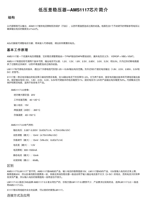
低压差稳压器--AMS1117芯⽚简介结构从内部框图可以看出,ASM1117提供电流限制和热保护(TSD),以防环境温度造成过⾼的结温。
电路包含1个齐纳调节的带隙参考电压以确保输出电压的精度在±1%以内。
ADJ引脚是可调整电压引脚,⽤来接⼊可调电阻,调出你所需要的电压。
基本⼯作原理AMS1117是⼀个低漏失电压调整器,它的稳压调整管是由⼀个PNP驱动的NPN管组成的,漏失电压定义为: VDROP = VBE+ VSAT。
AMS1117有固定和可调两个版本可⽤,输出电压可以是:1.2V,1.5V,1.8V,2.5V,2.85V, 3.0V,3.3V,和5.0V。
⽚内过热切断电路提供了过载和过热保护,以防环境温度造成过⾼的结温。
LM1117有可调电压的版本,通过2个外部电阻可实现1.25~13.8V输出电压范围。
另外还有5个固定电压输出(1.8V、2.5V、2.85V、3.3V和5V)的型号。
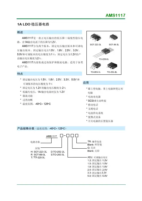
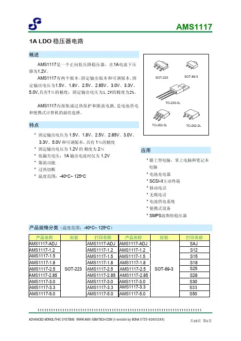
X1117是⼀款正电压输出的低压降三端线性稳压电路,在1A输出电流下的压降为1.2V。
分为两个版本,固定电压输出版本和可调电压输出版本。
固定输出电压1.5V、1.8V、2.5V、3.3V、5.0V和可调版本的电压精度为1%;固定电压为1.2V的产品输出电压精度为2%。
内部集成过热保护和限流电路,适⽤于各类电⼦产品。
AMS1117-3.3参数:绝对最⼤额定值:20V⼯作结温范围:-40~125°C输⼊电压:15V焊接温度(25秒):265°C存储温度:-65~150°CAMS1117-3.3电⽓特性:输出电压:3.267~3.333V(0≤IOUT≤1A,4.75V≤VIN≤12V)线性调整(最⼤):10mV(4.75V≤VIN≤12V)负载调节(最⼤):15mV(VIN=5V,0≤IOUT≤1A)电压差(最⼤):1.3V电流限制:900~1500mA静态电流(最⼤):10mA纹波抑制(最⼩):60dB。
ams1117热阻参数【原创实用版】目录1.AMS1117 概述2.热阻参数的定义与意义3.AMS1117 的热阻参数特性4.AMS1117 的应用领域5.结论正文一、AMS1117 概述AMS1117 是一款由德州仪器(TI)公司推出的 1.2A 同步降压 DC-DC 转换器,具有出色的性能和效率。
这款器件采用了恒定频率电流模式控制,可以实现高达 98% 的转换效率。
在众多的电源管理器件中,AMS1117 以其稳定的输出电压和广泛的应用领域而受到广泛关注。
二、热阻参数的定义与意义热阻参数,又称热阻系数,是指在给定温度差下,通过器件的电流与产生的热量之间的比值。
热阻参数是衡量器件散热性能的重要指标,直接影响到器件的可靠性和稳定性。
对于电源管理器件而言,热阻参数尤为重要,因为它们通常工作在高功率和高温环境。
三、AMS1117 的热阻参数特性AMS1117 的热阻参数特性如下:1.温度范围:AMS1117 的工作温度范围为 -40℃至 125℃。
在此温度范围内,器件的性能和稳定性得到保证。
2.热阻系数:AMS1117 的热阻系数为 4.5°C/W。
这意味着在 1W 的功耗下,通过器件的电流每增加 1A,器件的温度将上升 4.5°C。
3.散热设计:由于 AMS1117 具有较高的热阻参数,因此在应用过程中需要合理设计散热方案,以保证器件的可靠性和稳定性。
四、AMS1117 的应用领域AMS1117 广泛应用于各种电源管理领域,如通信设备、工业控制、网络设备、便携式电子设备等。
在这些应用中,AMS1117 的热阻参数特性对于保证系统的稳定运行具有重要意义。
五、结论综上所述,AMS1117 作为一款优秀的电源管理器件,在拥有较高转换效率的同时,也具备良好的热阻参数特性。
ams1117标准电路AMS1117是一种具有线性调节功能的低压差正压稳压器,常用于电子设备与电路中,用于稳定输出电压。
本文将介绍AMS1117的工作原理、应用场景及使用方法。
一、工作原理AMS1117是通过基准电压源、误差放大器、功率差分放大器、输出放大器、电流限制放大器和过温保护电路构成的。
其工作原理如下:1. 基准电压源产生稳定的基准电压;2. 误差放大器通过与基准电压进行比较,产生误差信号;3. 功率差分放大器将误差信号放大并与基准电压进行比较,得到控制信号;4. 输出放大器根据控制信号调节输出电压,使其保持在设定值。
二、应用场景AMS1117广泛应用于各种电子设备和电路中,常见的应用场景有:1. 数码产品:手机、平板电脑、相机等电子设备中,用于稳定供电,提供稳定的工作电压;2. 电源模块:无线路由器、电视机、音响等家电产品中,用于输出稳定的电源;3. 电子玩具:远程遥控车、无人机等电子玩具中,用于保证电路正常工作;4. 工业控制:自动化设备、机器人等工业控制领域中,用于提供可靠的电源供应。
三、使用方法AMS1117的使用方法如下:1. 输入电压:该芯片可以接受输入电压范围为4.5V至15V,推荐输入电压为6.5V至12V;2. 输出电压:可根据需要选择不同型号的AMS1117,常见的有3.3V和5V两种输出电压;3. 连接方式:将输入电压连接到芯片的输入端(VIN),输出电压连接到芯片的输出端(VOUT);4. 外部元件:为了保证稳压功能,可以在输入端并联一个电容和一个电阻;5. 热敏保险丝:为了保护芯片免受过热的影响,可以在输出端并联一个热敏保险丝。
四、常见问题及解决方法在使用AMS1117过程中,可能会遇到以下问题:1. 输出电压不稳定:可能是输入电压波动导致,请检查输入电压是否稳定,并合理选择输入电压范围;2. 过热现象:可能是负载过大导致芯片发热,请减小负载并加装热敏保险丝以保护芯片;3. 输出电压超过额定值:可能是输入电压超过芯片的额定值,请确保输入电压在合理范围内;4. 输出电压小于额定值:可能是负载过大导致,请减小负载并确保负载在芯片额定范围内。
ams1117 和lm1117 区别
AMS1117 与LM1117 只有厂家不同的区别,其他的没有区别。
AMS1117 是AMS 的产品,输入电压的极限值是15V,LM1117 是NS 的产品,15V 是输入电压的正常上限,极限值是20V,所以后者的耐压值要高一些,但是这类线性稳压器一般适合用于输入输出电压差不太大
(3~5V)的场合,否则电流大时效率低发热严重,所以输入电压的极限值高一些用途也不很大。
稳压到3.3V 应该选用1117 系列产品中后缀为3.3 的信号,如
AMS11173.3 或LM11173.3,只要输入电压在工作电压允许范围内,它们的输出电压都是3.3V。
AMS1117 系列稳压器有可调版与多种固定电压版,设计用于提供1A 输出电流且工作压差可低至1V。
在最大输出电流时,AMS1117 器件的压差保证最大不超过1.3V,并随负载电流的减小而逐渐降低。
ams1117标准电路ams1117是一款广泛应用于电子设备中的标准电路,其主要功能是提供稳定的电压输出。
本文将对ams1117的标准电路进行详细解析,包括其工作原理、应用领域、优缺点以及如何选择合适的电路。
一、ams1117简介ams1117是一款线性稳压器,由美国analog devices公司研发生产。
它具有内置短路保护和过温保护等特点,可提供稳定的电压输出,广泛应用于各种电子设备中。
二、ams1117电路原理ams1117电路采用线性稳压器技术,通过调整晶体管的导通程度来实现输出电压的稳定。
当输出电压低于设定值时,晶体管导通程度加大,使得输出电压上升;当输出电压高于设定值时,晶体管导通程度减小,使得输出电压下降。
这样,通过晶体管的导通程度的调整,实现输出电压的稳定。
三、ams1117应用领域ams1117的应用领域非常广泛,包括但不限于以下几个方面:1.电源模块:用于电子设备电源供应,如智能手机、平板电脑等;2.嵌入式系统:用于嵌入式设备的电压稳压,如智能家居、工业控制系统等;3.通信设备:用于通信设备的电压稳定,如路由器、交换机等;4.电动汽车:用于电动汽车的电池管理系统,确保电池电压稳定。
四、ams1117的优缺点ams1117的优点:1.输出电压稳定,具有良好的线性特性;2.内置短路保护和过温保护,提高了电路的可靠性;3.电源转换效率高,降低了能源损耗;4.体积小,便于集成。
缺点:1.工作温度范围有限,高温环境下性能可能受到影响;2.输出电流能力较低,不适用于大电流场合。
五、如何选择合适的ams1117电路在选择ams1117电路时,需要考虑以下几个方面:1.输出电压:根据设备需求选择合适的输出电压;2.输出电流:确保ams1117的输出电流大于设备所需的电流;3.工作温度范围:选择与设备工作环境相匹配的工作温度范围;4.封装形式:根据电路板空间和安装要求选择合适的封装形式。
六、结论ams1117标准电路凭借其稳定的电压输出、高效的转换率和良好的保护功能,广泛应用于各种电子设备中。
ams1117-3.3v电源稳压芯片低压差线性稳压器概述ams1117是一种高性能低压差线性稳压器,它采用了Bipolar工艺,具有输入电压范围宽、温度漂移小、线性度好等优点。
它适用于各种电子设备中的电源管理,尤其是对输入电压波动要求严格的应用。
ams1117-3.3v电源稳压芯片是一款输出电压为3.3V的芯片,由于现在很多电路都需要3.3V的输入电压,因此该芯片在电子设备中应用广泛。
技术参数•输入电压范围:4.5V~15V•输出电压:3.3V•输出电流:800mA•静态电流:5mA•线性度:±2%应用单片机电路单片机是目前工业控制和通信领域中应用最为广泛的微处理器,因此在单片机电路中,对于稳定的3.3V电压输入是必须的。
ams1117-3.3v电源稳压芯片可用于在单片机电路中,将输入电压稳定为3.3V。
电源模块ams1117-3.3v电源稳压芯片也可以在电源模块中起到重要的作用。
除了普通的DC/DC变换模块之外,一些需要3.3V电压输入的设备,如传感器和微控制器开发板,都可以使用该芯片来产生所需要的稳定3.3V电压。
无线通信电路无线通信技术是目前发展最为迅速、最为关键的技术之一,而在无线电路中,对输入电压的稳定性有着极高的要求。
ams1117-3.3v电源稳压芯片可以在无线电路中,通过过滤掉输入电压中的杂波和噪声,从而达到提升信噪比的作用。
光电子电路在光电子电路中,常常需要稳定的3.3V电压,而ams1117-3.3v电源稳压芯片的高性能和稳定性可以满足光电子电路的需求。
总结ams1117-3.3v电源稳压芯片是一种高性能低压差线性稳压器,适用于各种电子设备中的电源管理。
它具有输入电压范围宽、温度漂移小、线性度好等优点,在单片机电路、电源模块、无线通信电路、光电子电路等领域均有着广泛的应用。
ams1117热阻参数AMS1117是一种常用的线性稳压器芯片,广泛应用于电子设备中。
它的热阻参数是指在工作过程中,芯片内部产生的热量与外部环境之间的热阻。
了解AMS1117的热阻参数对于设计和使用电子设备非常重要。
首先,我们需要了解什么是热阻。
热阻是指物体传导热量的能力,单位是摄氏度每瓦特(℃/W)。
热阻越小,表示物体传导热量的能力越好,温度上升越小。
热阻参数是评估芯片散热性能的重要指标。
AMS1117芯片的热阻参数通常由两个值来表示:θJA和θJC。
其中,θJA表示芯片与周围环境之间的热阻,也称为热阻-环境。
θJC表示芯片与封装外壳之间的热阻,也称为热阻-封装。
AMS1117芯片的热阻参数与芯片的封装方式有关。
常见的封装方式有SOT-223、SOT-89等。
不同封装方式的芯片热阻参数可能会有所不同。
一般来说,SOT-223封装的AMS1117芯片的热阻参数较小,散热性能较好。
对于AMS1117芯片来说,热阻参数的大小直接影响芯片的工作温度。
热阻越小,芯片的工作温度越低,性能越稳定。
因此,在设计电子设备时,需要根据芯片的热阻参数来选择合适的散热措施,以确保芯片的正常工作。
在实际应用中,我们可以通过计算来估算AMS1117芯片的工作温度。
假设芯片的最大功率为Pmax,热阻参数为θJA,环境温度为Tambient,则芯片的工作温度可以通过以下公式计算:Tjunction = Tambient + Pmax * θJA通过这个公式,我们可以根据芯片的热阻参数和环境温度来估算芯片的工作温度。
如果工作温度超过芯片的额定温度范围,可能会导致芯片的性能下降甚至损坏。
因此,在设计和使用电子设备时,我们需要充分考虑芯片的热阻参数。
合理选择散热措施,如散热片、散热风扇等,以提高芯片的散热性能,确保设备的稳定工作。
总之,AMS1117芯片的热阻参数是评估芯片散热性能的重要指标。
了解芯片的热阻参数,可以帮助我们选择合适的散热措施,确保设备的正常工作。
ams1117标准电路
AMS1117是一种低压差线性稳压器,常用于电子设备中为芯
片提供稳定的电源供应。
它具有输入和输出之间的非常小的电压差,通常为1V左右。
AMS1117标准电路包括输入电容、
稳压器芯片、输出电容和钳位二极管。
1. 输入电容:为了保持输入电压的稳定性,通常会在
AMS1117的输入引脚上加一个电容。
这个电容可以起到滤波
和稳压的作用,帮助保持输入电压的平稳。
2. 稳压器芯片:AMS1117芯片是一个集成电路,负责将输入
电压(Vin)稳定为输出电压(Vout)。
它根据电路中的反馈控制算
法来调节输出电压,并且具有较高的稳定性和精度。
3. 输出电容:为了提供输出电压的稳定性,通常会在
AMS1117的输出引脚上加一个电容。
这个电容可以起到滤波
和稳压的作用,帮助保持输出电压的平稳。
4. 钳位二极管:钳位二极管是为了保护稳压器芯片和输出负载而设置的。
它可以防止输出电压超过稳压器芯片的额定电压和负载电流,从而保护电路的稳定性和可靠性。
通过以上组成部分的配合,AMS1117标准电路可以提供稳定
可靠的电源供应,适用于各种电子设备和电路。
它具有体积小、成本低、效率高等优点,在很多应用中得到广泛应用。
ams1117和lm1117区别AMS1117与LM1117只有厂家不同的区别,其他的没有区别。
AMS1117是AMS的产品,输入电压的极限值是15V,LM1117是NS的产品,15V是输入电压的正常上限,极限值是20V,所以后者的耐压值要高一些,但是这类线性稳压器一般适合用于输入输出电压差不太大(3~5V)的场合,否则电流大时效率低发热严重,所以输入电压的极限值高一些用途也不很大。
稳压到3.3V应该选用1117系列产品中后缀为—3.3的信号,如AMS1117—3.3或LM1117—3.3,只要输入电压在工作电压允许范围内,它们的输出电压都是3.3V。
AMS1117系列稳压器有可调版与多种固定电压版,设计用于提供1A输出电流且工作压差可低至1V。
在最大输出电流时,AMS1117器件的压差保证最大不超过1.3V,并随负载电流的减小而逐渐降低。
AMS1117的片上微调把基准电压调整到1.5%的误差以内,而且电流限制也得到了调整,以尽量减少因稳压器和电源电路超载而造成的压力。
AMS1117器件引脚上兼容其他三端SCSI稳压器,提供适用贴片安装的SOT-223,8引脚SOIC,和TO-252(DPAK)塑料封装。
AMS1117 参数 AMS1117 基本参数输出电流(A) 1 输出电压(V)Adj,1.2,1.5, 1.8, 2.5,2.85,3.3, 5.0, * AMS1117 其他特性初始误差(%)±1.5 压差(V) 1.3 AMS1117 封装类型 SOT-223 TO-252 SO-8 三端口可调节或固定输出电压1.2V,1.5V, 1.8V,2.5V, 2.85V,3.3V 和5.0V 输出电流1A 工作压差低至1V 线荷载调节:0.2% Max. 负载调节:0.4% Max. 可选SOT-223,TO-252和SO-8封装LM1117-3.3 是进口NS品牌AMS1117-3.3 是台湾生产的价格方面LM1117-3.3 也是要贵不少的产品要求要是比较高的话还是选择LM1117-3.3 一般的话AMS1117-3.3的可以了的。
最新AMS1117全系列解析AMS1117全系列是一款高性能的线性稳压器,广泛应用于各类电子设备中。
本文将为您详细解析AMS1117全系列的特点、应用及注意事项,帮助您更好地了解这款稳压器。
一、AMS1117全系列概述1. 输出电流:最大可达1A,满足大部分电子设备的需求。
2. 线性稳压:采用线性稳压技术,具有低噪声、高稳定性等优点。
3. 固定/可调输出:根据不同型号,提供固定电压或可调电压输出。
4. 宽电压输入范围:输入电压范围为4.5V至12V,适应多种电源环境。
5. 封装形式:采用SOT223、SOT89等封装,便于安装和使用。
二、AMS1117全系列应用场景1. AMS11173.3:适用于3.3V供电的嵌入式系统、通信设备、数码产品等。
2. AMS11175.0:适用于5V供电的电子产品,如单片机、传感器、各类模块等。
3. AMS1117adj:可根据实际需求调整输出电压,适用于电源模块、充电器等场合。
三、AMS1117全系列注意事项1. 安装时,注意散热:由于AMS1117全系列采用线性稳压技术,发热量较大,建议在安装时留出足够的散热空间,或使用散热器。
3. 调整电阻选择:对于AMS1117adj型号,需外接两个电阻来调整输出电压。
根据所需输出电压和公式计算合适的电阻值,以确保稳压器正常工作。
四、AMS1117全系列优势分析1. 高效率与稳定性:AMS1117全系列稳压器在提供稳定输出电压的同时,保持了较高的效率,减少了能量损耗,提升了系统的整体性能。
2. 优异的负载调整率:即使在负载变化较大的情况下,AMS1117全系列也能保持输出电压的稳定,这对于负载波动较大的应用场合尤为重要。
3. 过温保护:内置过温保护功能,当温度超过安全范围时,稳压器会自动关闭输出,保护电路不受损害。
4. 输出电流限制:AMS1117全系列具有内置的输出电流限制功能,防止过载情况下的永久性损坏。
五、AMS1117全系列在实际应用中的案例1. 移动电源:使用AMS11175.0稳压器,为移动电源提供稳定的5V输出,确保充电设备的兼容性和安全性。
Advanced AMS1117 Monolithic 800mA LOW DROPOUT VOLTAGE REGULATORSystemsFEATURESAPPLICATIONS• Three Terminal Adjustable or Fixed Voltages*• High Efficiency Linear Regulators 1.5V, 1.8V, 2.5V, 2.85V, 3.3V and 5.0V • Post Regulators for Switching Supplies • Output Current of 800mA • 5V to 3.3V Linear Regulator • Operates Down to 1V Dropout • Battery Chargers• Line Regulation: 0.2% Max.• Active SCSI Terminators• Load Regulation: 0.4% Max.• Power Management for Notebook • SOT-223 and TO-252 package available• Battery Powered InstrumentationGENERAL DESCRIPTIONThe The AMS1117 series of adjustable and fixed voltage regulators are designed to provide 800mA output current and to operate down to 1V input-to-output differential. The dropout voltage of the device is guaranteed maximum 1.3V at maximum output current, decreasing at lower load currents.On-chip trimming adjusts the reference voltage to 1%. Current limit is also trimmed, minimizing the stress under overload conditions on both the regulator and power source circuitry.The AMS1117 devices are pin compatible with other three-terminal SCSI regulators and are offered in the low profile surface mount SOT-223 package and in the TO-252 (DPAK) plastic package.ORDERING INFORMATION:PACKAGE TYPEOPERATING JUNCTIONTO-252SOT-223TEMPERATURE RANGEAMS1117CD AMS11170 to 125° C AMS1117CD-1.5 AMS1117-1.50 to 125°C AMS1117CD-1.8 AMS1117-1.80 to 125° C AMS1117CD-2.5 AMS1117-2.50 to 125° C AMS1117CD-2.85 AMS1117-2.850 to 125° C AMS1117CD-3.3 AMS1117-3.30 to 125° C AMS1117CD-5.0 AMS1117-5.00 to 125° C *For additional available fixed voltages contact factory.PIN CONNECTIONSFIXED VERSION ADJUSTABLE VERSION 1- Ground 2- V OUT 3- V IN1- Adjust 2- V OUT 3- V INAMS1117 ABSOLUTE MAXIMUM RATINGS (Note 1)Power Dissipation Internally limited Soldering informationInput Voltage 15V Lead Temperature (10 sec) 300°C Operating Junction Temperature Ra Thermal ResistanceControl Section0°C to 125°C TO-252 packageϕJA= 80°C/W Power Transistor 0°C to 150°C SOT-223 packageϕJA= 90°C/W* Storage temperature- 65°C to +150°C* With package soldering to copper area over backsideground plane or internal power plane ϕJA can vary from46°C/W to >90°C/W depending on mounting technique andthe size of the copper area.ELECTRICAL CHARACTERISTICSElectrical Characteristics at I OUT = 0 mA, and T J = +25°C unless otherwise specified.Parameter Device Conditions Min Typ Max UnitsReference Voltage (Note 2)AMS1117I OUT = 10 mA10mA ≤ I OUT≤ 800mA, 1.5V≤ (V IN - V OUT) ≤ 12V1.2381.2251.2501.2501.2621.270VVOutput Voltage (Note 2)AMS1117-1.50 ≤ I OUT≤ 800mA , 3.0V≤ V IN≤ 12V 1.4851.4761.5001.5001.5151.524VV AMS1117-1.80 ≤ I OUT≤ 800mA , 3.3V≤ V IN≤ 12V 1.7821.7731.8001.8001.8181.827VV AMS1117-2.50 ≤ I OUT≤ 800mA , 4.0V≤ V IN≤ 12V 2.4752.4602.5002.5002.5252.560VV AMS1117-2.850 ≤ I OUT≤ 800mA , 4.35V≤ V IN≤ 12V 2.822.792.8502.8502.882.91VV AMS1117-3.30 ≤ I OUT≤ 800mA , 4.75V ≤ V IN≤ 12V 3.2673.2353.3003.3003.3333.365VV AMS1117-5.00 ≤ I OUT≤ 800mA , 6.5V ≤ V IN≤ 12V 4.9504.9005.0005.0005.0505.100VVLine Regulation AMS1117 I LOAD = 10 mA , 1.5V≤ (V IN - V OUT) ≤ 12V0.0150.0350.20.2%%AMS1117-1.5 3.0V≤ V IN≤ 12V0.30.656mVmVAMS1117-1.8 3.3V≤ V IN≤ 12V0.30.656mVmVAMS1117-2.5 4.0V≤ V IN≤ 12V0.30.666mVmVAMS1117-2.85 4.35V≤ V IN≤ 12V0.30.666mVmVAMS1117-3.3 4.75V≤ V IN≤ 12V0.51.01010mVmVAMS1117-5.0 6.5V≤ V IN≤ 12V0.51.01010mVmVLoad Regulation (Notes 2, 3)AMS1117(V IN - V OUT) =3V, 10mA ≤ I OUT≤ 800mA0.10.20.30.4%% AMS1117-1.5V IN = 5V, 0 ≤ I OUT≤ 800mA361020mVmV AMS1117-1.8V IN = 5V, 0 ≤ I OUT≤ 800mA361020mVmV AMS1117-2.5V IN = 5V, 0 ≤ I OUT≤ 800mA361220mVmVELECTRICAL CHARACTERISTICSElectrical Characteristics at I OUT = 0 mA, and T J = +25°C unless otherwise specified.Parameter Device Conditions Min Typ Max UnitsLoad Regulation (Notes 2, 3)AMS1117-2.85V IN = 5V, 0 ≤ I OUT≤ 800mA361220mVmV AMS1117-3.3V IN = 5V, 0 ≤ I OUT≤ 800mA371525mVmV AMS1117-5.0V IN = 8V, 0 ≤ I OUT≤ 800mA5102035mVmVDropout Voltage (V IN - V OUT)AMS1117-1.5/-1.8/-2.5/-2.85/-3.3/-5.0∆V OUT , ∆V REF = 1%, I OUT = 800mA (Note 4) 1.1 1.3VCurrent Limit AMS1117-1.5/-1.8/-2.5/-2.85/-3.3/-5.0(V IN - V OUT) = 5V9001,1001,500mAMinimum LoadCurrentAMS1117(V IN - V OUT) = 12V (Note 5)510mAQuiescent Current AMS1117-1.5/-1.8/-2.5/-2.85/-3.3/-5.0V IN≤ 12V510mARipple Rejection AMS1117 f =120Hz , C OUT = 22µF Tantalum, I OUT = 800mA,(V IN-V OUT ) = 3V, C ADJ =10µF6075dBAMS1117-1.5/-1.8/-2.5/-2.85f =120Hz , C OUT = 22µF Tantalum, I OUT = 800mA,V IN = 6V6072dBAMS1117-3.3 f =120Hz , C OUT = 22µF Tantalum, I OUT = 800mAV IN = 6.3V6072dBAMS1117-5.0 f =120Hz , C OUT = 22µF Tantalum, I OUT = 800mAV IN = 8V6068dB Thermal Regulation AMS1117T A = 25°C, 30ms pulse0.0080.04%WAdjust Pin Current AMS111710mA ≤ I OUT≤ 800mA , 1.5V≤ (V IN - V OUT) ≤ 12V55120µA µAAdjust Pin CurrentChangeAMS111710mA ≤ I OUT≤ 800mA , 1.5V≤ (V IN - V OUT) ≤ 12V0.25µA Temperature Stability0.5% Long Term Stability T A =125°C, 1000Hrs0.31% RMS Output Noise(% of V OUT )T A = 25°C , 10Hz ≤ f ≤ 10kHz0.003%Thermal ResistanceJunction-to-Case15°C/WParameters identified with boldface type apply over the full operating temperature range.Note 1:Absolute Maximum Ratings indicate limits beyond which damage to the device may occur. For guaranteed specifications and test conditions, see the Electrical Characteristics. The guaranteed specifications apply only for the test conditions listed.Note 2: Line and Load regulation are guaranteed up to the maximum power dissipation of 1.2 W. Power dissipation is determined by the input/output differential and the output current. Guaranteed maximum power dissipation will not be available over the full input/output range.Note 3: See thermal regulation specifications for changes in output voltage due to heating effects. Line and load regulation are measured at a constant junction temperature by low duty cycle pulse testing. Load regulation is measured at the output lead ~1/8” from the package.Note 4: Dropout voltage is specified over the full output current range of the device.Note 5:Minimum load current is defined as the minimum output current required to maintain regulation. When 1.5V ≤ (V IN - V OUT) ≤ 12V the device is guaranteed to regulate if the output current is greater than 10mA.APPLICATION HINTSThe AMS1117 series of adjustable and fixed regulators are easy to use and are protected against short circuit and thermal overloads. Thermal protection circuitry will shut-down theregulator should the junction temperature exceed 165°C at the sense point.Pin compatible with older three terminal adjustable regulators, these devices offer the advantage of a lower dropout voltage, more precise reference tolerance and improved reference stability with temperature.StabilityThe circuit design used in the AMS1117 series requires the use of an output capacitor as part of the device frequency compensation. The addition of22µF solid tantalum on the output will ensure stability for all operating conditions.When the adjustment terminal is bypassed with a capacitor to improve the ripple rejection, the requirement for an output capacitor increases. The value of 22µF tantalum covers all cases of bypassing the adjustment terminal. Without bypassing the adjustment terminal smaller capacitors can be used with equally good results.To ensure good transient response with heavy load current changes capacitor values on the order of 100µF are used in the output of many regulators. To further improve stability and transient response of these devices larger values of output capacitor can be used.Protection DiodesUnlike older regulators, the AMS1117 family does not need any protection diodes between the adjustment pin and the output and from the output to the input to prevent over-stressing the die. Internal resistors are limiting the internal current paths on the AMS1117 adjustment pin, therefore even with capacitors on the adjustment pin no protection diode is needed to ensure device safety under short-circuit conditions.Diodes between the input and output are not usually needed. Microsecond surge currents of 50A to 100A can be handled by the internal diode between the input and output pins of the device. In normal operations it is difficult to get those values of surge currents even with the use of large output capacitances. If high value output capacitors are used, such as 1000µF to 5000µF and the input pin is instantaneously shorted to ground, damage can occur. A diode from output to input is recommended, when a crowbar circuit at the input of the AMS1117 is used (Figure 1).FVOUTD1VINFigure 1.Output VoltageThe AMS1117 series develops a 1.25V reference voltage between the output and the adjust terminal. Placing a resistor between these two terminals causes a constant current to flow through R1 and down through R2 to set the overall output voltage. This current is normally the specified minimum load current of 10mA. Because I ADJ is very small and constant itrepresents a small error and it can usually be ignored.VOUT VINV OUT = V REF (1+ R2/R1)+I ADJ R2Figure 2. Basic Adjustable RegulatorLoad RegulationTrue remote load sensing it is not possible to provide, because the AMS1117 is a three terminal device. The resistance of the wire connecting the regulator to the load will limit the load regulation. The data sheet specification for load regulation is measured at the bottom of the package. Negative side sensing is a true Kelvin connection, with the bottom of the output divider returned to the negative side of the load.The best load regulation is obtained when the top of the resistor divider R1 is connected directly to the case not to the load. If R1 were connected to the load, the effective resistance between the regulator and the load would be:R P x( R2+R1 ) , R P = Parasitic Line Resistance R1APPLICATION HINTSConnected as shown , R P is not multiplied by the divider ratioR LV INR PPARASITIC *CONNECT R1 TO CASECONNECT R2 TO LOADFigure 3. Connections for Best Load RegulationIn the case of fixed voltage devices the top of R1 is connectedKelvin internally, and the ground pin can be used for negative side sensing.Thermal ConsiderationsThe AMS1117 series have internal power and thermal limiting circuitry designed to protect the device under overload conditions.However maximum junction temperature ratings of 125°C should not be exceeded under continuous normal load conditions.Careful consideration must be given to all sources of thermal resistance from junction to ambient. For the surface mount package SOT-223 additional heat sources mounted near the device must be considered. The heat dissipation capability of the PC board and its copper traces is used as a heat sink for the device. The thermal resistance from the junction to the tab for the AMS1117 is 15°C/W. Thermal resistance from tab to ambient can be as low as 30°C/W.The total thermal resistance from junction to ambient can be as low as 45°C/W. This requires a reasonable sized PC board with at least on layer of copper to spread the heat across the board and couple it into the surrounding air.Experiments have shown that the heat spreading copper layer does not need to be electrically connected to the tab of the device.The PC material can be very effective at transmitting heat between the pad area, attached to the pad of the device, and a ground plane layer either inside or on the opposite side of the board. Although the actual thermal resistance of the PC material is high, the Length/Area ratio of the thermal resistance between layers is small. The data in Table 1, was taken using 1/16” FR-4board with 1 oz. copper foil, and it can be used as a rough guideline for estimating thermal resistance.For each application the thermal resistance will be affected by thermal interactions with other components on the board. To determine the actual value some experimentation will be necessary.The power dissipation of the AMS1117 is equal to:P D = ( V IN - V OUT )( I OUT )Maximum junction temperature will be equal to:T J = T A(MAX) + P D (Thermal Resistance (junction-to-ambient))Maximum junction temperature must not exceed 125°C.Ripple RejectionThe ripple rejection values are measured with the adjustment pin bypassed. The impedance of the adjust pin capacitor at the ripple frequency should be less than the value of R1 (normally 100Ω to 200Ω) for a proper bypassing and ripple rejection approaching the values shown. The size of the required adjust pin capacitor is a function of the input ripple frequency. If R1=100Ω at 120Hz the adjust pin capacitor should be >13µF. At 10kHz only 0.16µF is needed.The ripple rejection will be a function of output voltage, in circuits without an adjust pin bypass capacitor. The output ripple will increase directly as a ratio of the output voltage to the reference voltage (V OUT / V REF ).Table 1.COPPER AREATHERMAL RESISTANCE TOP SIDE*BACK SIDE BOARD AREA (JUNCTION-TO-AMBIENT)2500 Sq. mm 2500 Sq. mm 2500 Sq. mm 45°C/W 1000 Sq. mm 2500 Sq. mm 2500 Sq. mm 45°C/W 225 Sq. mm 2500 Sq. mm 2500 Sq. mm 53°C/W 100 Sq. mm 2500 Sq. mm 2500 Sq. mm 59°C/W 1000 Sq. mm 1000 Sq. mm 1000 Sq. mm 52°C/W 1000 Sq. mm 01000 Sq. mm 55°C/W* Tab of device attached to topside copper.TYPICAL PERFORMANCE CHARACTERISTICSMinimum Operating Current (Adjustable Device)Short-Circuit CurrentLoad RegulationRipple Rejection vs. CurrentAdjust Pin CurrentTemperature Stability5101520036912INPUT/OUTPUT DIFFERENTIAL (V)51015M I N I M U M O P E R A T I N G C U R R E N T (m A )INPUT/OUTPUT DIFFERENTIAL00.250.500.751.001.25S H O R T C I R C U I T C U R R E N T (A )-50-25255075100125-0.20-0.15-0.10-0.050.050.10TEMPERATURE (°C)O U T P U T V O L T A G E D E V I A T I O N (%)0.20.40.60.80102030405060708090100OUTPUT CURRENT (A)R I P P L E R E J E C T I O N (d B )-50-25255075100125150-2.0-1.01.02.0TEMPERATURE (°C)O U T P U T V O L T A G E C H A N G E (%)TEMPERATURE (°C)-50-2502550751001251500102030405060708090100A D J U S T P I N C U R R E N T (µA )PACKAGE DIMENSIONS inches (millimeters) unless otherwise noted.TO-252 PLASTIC PACKAGE (D)3 LEAD SOT-223 PLASTIC PACKAGE45.0°0.181(4.60)NOM10°MAX10°-16°10°-16°(SOT-223 ) AMS DRW# 042292。