General Description
The MAX3040–MAX3045 is a family of 5V quad RS-485/RS-422 transmitters designed for digital data trans-mission over twisted-pair balanced lines. All transmitter outputs are protected to ±10kV using the Human Body Model. In addition the MAX3040–MAX3045 withstand ±4kV per IEC 1000-4-4 Electrical Fast Transient/Burst Stressing. The MAX3040/MAX3043 (250kbps) and the MAX3041/MAX3044 (2.5Mbps) are slew-rate limited transmitters that minimize EMI and reduce reflections caused by improperly terminated cables, thus allowing error-free transmission.
The MAX3040–MAX3045 feature a hot-swap capability*that eliminates false transitions on the data cable during power-up or hot insertion. The MAX3042B/MAX3045B are optimized for data transfer rates up to 20Mbps, the MAX3041/MAX3044 for data rates up to 2.5Mbps, and the MAX3040/MAX3043 for data rates up to 250kbps.The MAX3040–MAX3045 offer optimum performance when used with the MAX3093E or MAX3095 5V quad differential line receivers or MAX3094E/MAX3096 3V quad differential line receivers.
The MAX3040–MAX3045 are ESD-protected pin-compat-ible, low-power upgrades to the industry-standard ‘SN75174 and ‘DS26LS31C. They are available in space-saving TSSOP, narrow SO, and wide SO packages.
*Patent pending
Applications
Telecommunications Equipment Industrial Motor Control
Transmitter for ESD-Sensitive Applications Hand-Held Equipment Industrial PLCs Networking
Features
o ESD Protection: ±10kV—Human Body Model o Single +5V Operation
o Guaranteed Device-to-Device Skew
(MAX3040/MAX3041/MAX3043/MAX3044)o Pin-Compatible with ‘SN75174, ‘26LS31C and LTC487o Hot-Swappable for Telecom Applications o Up to 20Mbps Data Rate (MAX3042B/MAX3045B)o Slew-Rate Limited (Data Rates at 2.5Mbps and 250kbps)o 2nA Low-Power Shutdown Mode o 1mA Operating Supply Current
o ±4kV EFT Fast Transient Burst Immunity per IEC 1000-4-4o Level 2 Surge Immunity per IEC 1000-4-5,Unshielded Cable Model o Ultra-Small 16-Pin TSSOP, 16-Pin Narrow SO, and Wide 16-Pin SO
MAX3040–MAX3045
±10kV ESD-Protected, Quad 5V RS-485/RS-422
Transmitters
________________________________________________________________Maxim Integrated Products
1
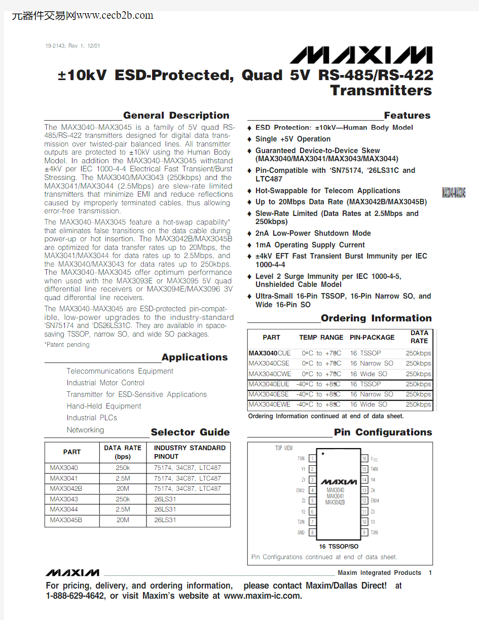
Pin Configurations
Selector Guide
Ordering Information
19-2143; Rev 1; 12/01
Ordering Information continued at end of data sheet.
For pricing, delivery, and ordering information,please contact Maxim/Dallas Direct!at 1-888-629-4642, or visit Maxim’s website at https://www.doczj.com/doc/0215433304.html,.
M A X 3040–M A X 3045
±10kV ESD-Protected, Quad 5V RS-485/RS-422Transmitters
ABSOLUTE MAXIMUM RATINGS
ELECTRICAL CHARACTERISTICS
Stresses beyond those listed under “Absolute Maximum Ratings” may cause permanent damage to the device. These are stress ratings only, and functional operation of the device at these or any other conditions beyond those indicated in the operational sections of the specifications is not implied. Exposure to absolute maximum rating conditions for extended periods may affect device reliability.
All voltages referenced to ground (GND).
Supply Voltage (V CC ).............................................................+7V Control Input Voltage (EN, EN , EN_) .........-0.3V to (V CC + 0.3V)Driver Input Voltage (T_IN).........................-0.3V to (V CC + 0.3V)Driver Output Voltage (Y_, Z_)
(Driver Disabled).............................................-7.5V to +12.5V Driver Output Voltage (Y_, Z_)
(Driver Enabled).................................................-7.5V to +10V Continuous Power Dissipation (T A = +70°C)
16-Pin TSSOP (derate 9.4mW/°C above +70°C)..........755mW
16-Pin Narrow SO (derate 8.70mW/°C above +70°C)..696mW 16-Pin Wide SO (derate 9.52mW/°C above +70°C).....762mW Operating Temperature Range
MAX304_C_E.......................................................0°C to +70°C MAX304_E_E....................................................-40°C to +85°C Maximum Junction Temperature.....................................+150°C Storage Temperature Range.............................-65°C to +150°C Lead Temperature (soldering, 10s).................................+300°C
MAX3040–MAX3045
±10kV ESD-Protected, Quad 5V RS-485/RS-422
Transmitters
SWITCHING CHARACTERISTICS —MAX3040/MAX3043
SWITCHING CHARACTERISTICS —MAX3041/MAX3044
M A X 3040–M A X 3045
±10kV ESD-Protected, Quad 5V RS-485/RS-422Transmitters 4_______________________________________________________________________________________
Note 2:?V OD and ?V OC are the changes in V OD and V OC , respectively, when the transmitter input changes state.
Note 3:This input current level is for the hot-swap enable (EN_, EN, EN ) inputs and is present until the first transition only. After the
first transition the input reverts to a standard high-impedance CMOS input with input current I IN . For the first 20μs the input current may be as high as 1mA. During this period the input is disabled.
Note 4:Maximum current level applies to peak current just prior to foldback-current limiting. Minimum current level applies during
current limiting.
SWITCHING CHARACTERISTICS —MAX3041/MAX3044 (continued)
(V CC = +5V ±5%, T A = T MIN to T MAX , unless otherwise noted. Typical values are at V CC = +5V and T A = +25°C.)
OUTPUT LOW VOLTAGE (V)
O U T P U T C U R R E N T (m A )
54-6-5-4-2-1012-331020304050
6070800
-76
OUTPUT CURRENT vs. TRANSMITTER
OUTPUT HIGH VOLTAGE
0.7
0.8
1.0
0.9
1.11.2
20
10
30
40
50
60
70
SUPPLY CURRENT vs. TEMPERATURE
TEMPERATURE (°C)
S U P P L Y C U R
R E N T (m A )
100
10000105152025353040450.1
1
10MAX3040/MAX3043
SUPPLY CURRENT vs. DATA RATE
DATA RATE (kbps)
S U P P L Y C U R R E N T (m A )
400
0.1110100100010,000MAX3041/MAX3044
SUPPLY CURRENT vs. DATA RATE
DATA RATE (kbps)S U P P L Y C U R R E N T (
m A )
1052015353025MAX3042B/MAX3045B
SUPPLY CURRENT vs. DATA RATE
DATA RATE (kbps)
0.1100100010,000110100,000
S U P P L Y C U R R E N T (m A )
600
10
203050400
20104030605070
0426810
OUTPUT CURRENT vs. TRANSMITTER
OUTPUT LOW VOLTAGE
OUTPUT LOW VOLTAGE (V)
O U T P U T C U R R E N T (m A )
MAX3040–MAX3045
±10kV ESD-Protected, Quad 5V RS-485/RS-422
Transmitters
_______________________________________________________________________________________5
Typical Operating Characteristics
(V CC = +5V, T A = +25°C, unless otherwise noted.)
0201040306050700
2
1
3
4
5
OUTPUT CURRENT
vs. DIFFERENTIAL OUTPUT VOLTAGE
M A X 3040 t o
c 07
DIFFERENTIAL OUTPUT VOLTAGE (V)
O U T P U T C U R R E N T (m A )
2.10
2.202.15
2.352.302.252.502.452.402.55
20
30
10
40
50
60
70
TRANSMITTER DIFFERENTIAL OUTPUT
VOLTAGE vs. TEMPERATURE
TEMPERATURE (°C)
D I F F
E R E N T I A L O U T P U T V O L T A G E (V )
M A X 3040–M A X 3045
±10kV ESD-Protected, Quad 5V RS-485/RS-422Transmitters 6_______________________________________________________________________________________
MAX3040–MAX3045
±10kV ESD-Protected, Quad 5V RS-485/RS-422
Transmitters
7
Detailed Description
The MAX3040–MAX3045 are quad RS-485/RS-422 trans-mitters. They operate from a single +5V power supply and are designed to give optimum performance when used with the MAX3093E/MAX3095 5V quad RS-485/RS-422 receivers or MAX3094E/MAX3096 3V quad RS-485/RS-422 receivers. The MAX3040–MAX3045 only need 1mA of operating supply current and consume 2nA when they enter a low-power shutdown mode. The MAX3040–MAX3045 also feature a hot-swap capability allowing line insertion without erroneous data transfer.The MAX3042B/MAX3045B are capable of transferring data up to 20Mbps, the MAX3041/MAX3044 for data rates up to 2.5Mbps, and the MAX3040/MAX3043 for data rates up to 250kbps. All transmitter outputs are pro-tected to ±10kV using the Human Body Model.
±10kV ESD Protection
As with all Maxim devices, ESD-protection structures are incorporated on all pins to protect against electro-static discharges (ESD) encountered during handling and assembly. The MAX3040–MAX3045 transmitter outputs have extra protection against electrostatic dis-charges found in normal operation. Maxim ’s engineers have developed state-of-the-art structures to protect these pins against the application of ±10kV ESD (Human Body Model), without damage.
ESD Test Conditions
ESD performance depends on a number of conditions.Contact Maxim for a reliability report that documents test setup, methodology, and results.
Human Body Model
Figure 6a shows the Human Body Model, and Figure 6b shows the current waveform it generates when dis-charged into low impedance. This model consists of a 100pF capacitor charged to the ESD voltage of interest,which is then discharged into the device through a 1.5k ?resistor.
Machine Model
The Machine Model for ESD testing uses a 200pF stor-age capacitor and zero-discharge resistance. It mimics the stress caused by handling during manufacturing and assembly. Of course, all pins (not just RS-485inputs) require this protection during manufacturing.Therefore, the Machine Model is less relevant to the I/O ports than are the Human Body Model.
±4kV Electrical Fast Transient/Burst Testing
(IEC 1000-4-4)
IEC 1000-4-4 Electrical Fast Transient/Burst (EFT/B) is an immunity test for the evaluation of electrical and electronic systems during operating conditions. The test was adapted for evaluation of integrated circuits with power applied. Repetitive fast transients with severe pulsed EMI were applied to signal and control ports. Over 15,000 distinct discharges per minute are sent to each interface port of the IC or equipment under test (EUT) simultaneously with a minimum test duration time of one minute. This simulates stress due to dis-placement current from electrical transients on AC mains, or other telecommunication lines in close prox-imity. Short rise times and very specific repetition rates are essential to the validity of the test.
Stress placed on the EUT is severe. In addition to the controlled individual discharges placed on the EUT,extraneous noise and ringing on the transmission line can multiply the number of discharges as well as increase the magnitude of each discharge. All cabling was left unterminated to simulate worst-case reflections.The MAX3040–MAX3045 were setup as specified in IEC 1000-4-4 and the Typical Operating Circuit of this data sheet. The amplitude, pulse rise time, pulse dura-tion, pulse repetition period, burst duration, and burst period (Figure 8)of the burst generator were all verified with a digital oscilloscope according to the specifica-tions in IEC 1000-4-4 sections 6.1.1 and 6.1.2. A simpli-fied diagram of the EFT/B generator is shown in Figure 7. The burst stresses were applied to Y1–Y4 and Z1–Z4simultaneously.
IEC 1000-4-4 provides several levels of test severity (see Table 1). The MAX3040–MAX3045 pass the 4000V stress, a special category “X ” beyond the highest level for severe (transient) industrial environments for telecommunication lines.
M A X 3040–M A X 3045
±10kV ESD-Protected, Quad 5V RS-485/RS-422Transmitters 8_______________________________________________________________________________________
MAX3040–MAX3045
±10kV ESD-Protected, Quad 5V RS-485/RS-422
Transmitters
_______________________________________________________________________________________
9
IEC 1000-4-4 Burst/Electrical Fast
Transient Test Levels (For Communication Lines)
The stresses are applied while the MAX3040–MAX3045are powered up. Test results are reported as:
1)Normal performance within the specification limits.2)Temporary degradation or loss of function or perfor-mance which is self-recoverable.3)Temporary degradation, loss of function or perfor-mance requiring operator intervention, such as sys-tem reset.4)Degradation or loss of function not recoverable due to damage.
The MAX3040–MAX3045 meets classification 2 listed above. Additionally, the MAX3040–MAX3045 will not latchup during the IEC burst stress events.
Hot-Swap Capability
Hot-Swap Inputs
When circuit boards are plugged into a “hot ” back-plane, there can be disturbances to the differential sig-nal levels that could be detected by receivers connected to the transmission line. This erroneous data could cause data errors to an RS-485/RS-422 system.To avoid this, the MAX3040–MAX3045 have hot-swap capable inputs.
When a circuit board is plugged into a “hot ” backplane there is an interval during which the processor is going through its power-up sequence. During this time, the processor ’s output drivers are high impedance and will be unable to drive the enable inputs of the MAX3040–MAX3045 (EN, EN , EN_) to defined logic lev-els. Leakage currents from these high impedance dri-vers, of as much as 10μA, could cause the enable inputs of the MAX3040–MAX3045 to drift high or low.Additionally, parasitic capacitance of the circuit board could cause capacitive coupling of the enable inputs to either G ND or V CC . These factors could cause the enable inputs of the MAX3040–MAX3045 to drift to lev-els that may enable the transmitter outputs (Y_ and Z_).To avoid this problem, the hot-swap input provides a method of holding the enable inputs of the MAX3040–MAX3045 in the disabled state as V CC ramps up. This hot-swap input is able to overcome the leakage currents and parasitic capacitances that may pull the enable inputs to the enabled state.
Hot-Swap Input Circuitry
In the MAX3040–MAX3045 the enable inputs feature hot-swap capability. At the input there are two NMOS
devices, Q1 and Q2 (Figure 9). When V CC is ramping up from 0, an internal 10μs timer turns on Q2 and sets the SR latch, which also turns on Q1. Transistors Q2, a 700μA current sink, and Q1, an 85μA current sink, pull EN to GND through a 5.6k ?resistor. Q2 is designed to pull the EN input to the disabled state against an exter-nal parasitic capacitance of up to 100pF that is trying to enable the EN input. After 10μs, the timer turns Q2 off and Q1 remains on, holding the EN input low against three-state output leakages that might enable EN. Q1remains on until an external source overcomes the
M A X 3040–M A X 3045
required input current. At this time the SR latch resets and Q1 turns off. When Q1 turns off, EN reverts to a standard, high-impedance CMOS input. Whenever V CC drops below 1V, the hot-swap input is reset.
The EN12 and EN34 input structures are identical to the EN input. For the EN input, there is a complimentary cir-cuit employing two PMOS devices pulling the EN input to V CC .
Hot-Swap Line Transient
The circuit of Figure 10 shows a typical offset termina-tion used to guarantee a greater than 200mV offset when a line is not driven. The 50pF represents the mini-mum parasitic capacitance which would exist in a typi-cal application. In most cases, more capacitance exists in the system and will reduce the magnitude of the glitch. During a “hot-swap ” event when the driver is connected to the line and is powered up, the driver must not cause the differential signal to drop below 200mV. Figures 11 and 12 show the results of the MAX3040–MAX3045 during power-up for two different V CC ramp rates (0.1V/μs and 1V/μs). The photos show the V CC ramp, the single-ended signal on each side of the 100?termination, the differential signal across the termination, and shows the hot-swap line transient stays above the 200mV RS-485 specification.
Operation of Enable Pins
The MAX3040–MAX3045 family has two enable-func-tional versions:
The MAX3040/MAX3041/MAX3042B have two transmit-ter enable inputs EN12 and EN34. EN12 controls the transmitters 1 and 2, and EN34 controls transmitters 3and 4. EN12 and EN34 are active-high and the part will enter the low-power shutdown mode when both are pulled low. The transmitter outputs are high impedance when disabled (Table 2).
The MAX3043/MAX3044/MAX3045B have two transmit-ter enable inputs EN and EN , which are active-high and active-low, respectively. When EN is logic high or EN is logic low all transmitters are active. When EN is pulled low and EN is driven high, all transmitters are disabled and the part enters the low-power shutdown mode. The transmitter outputs are high impedance when disabled (Table 3).
Applications Information
Typical Applications
The MAX3040–MAX3045 offer optimum performance when used with the MAX3093E/MAX3095 5V quad receivers or MAX3094E/MAX3096 3V quad differential line receivers. Figure 13 shows a typical RS-485 con-nection for transmitting and receiving data and Figure 14 shows a typical multi-point connection.
±10kV ESD-Protected, Quad 5V RS-485/RS-422Transmitters 10______________________________________________________________________________________
Figure 9. Simplified Structure of the Driver Enable Pin (EN)
MAX3040–MAX3045
±10kV ESD-Protected, Quad 5V RS-485/RS-422
Transmitters
______________________________________________________________________________________11
V CC 2V/div Y-Z
(20mV/div)238mV
Y
200mV/div Z
200mV/div Figure 11. Differential Power-Up Glitch (0.1V/μs)
V CC 2V/div Y-Z
(5mV/div)238mV
Y
50mV/div Z
50mV/div 1μs/div
Figure 12. Differential Power-Up Glitch (1V/μs)
Figure 10. Differential Power-Up Glitch (Hot Swap)
M A X 3040–M A X 3045
±10kV ESD-Protected, Quad 5V RS-485/RS-422Transmitters 12______________________________________________________________________________________
Typical Multiple-Point Connection
Figure 14 shows a typical multiple-point connection for the MAX3040–MAX3045 with the MAX3095. Because of the high frequencies and the distances involved, high attention must be paid to transmission-line effects while using termination resistors. A terminating resistor (RT)is simply a resistor that should be placed at the extreme ends of the cable to match the characteristic impedance of the cable. When the termination resis-tance is not the same value as the characteristic impedance of the cable, reflections will occur as the signal is traveling down the cable. Although some reflections are inevitable due to the cable and resistor tolerances, large mismatches can cause significant reflections resulting in errors in the data. With this in mind, it is very important to match the terminating resis-tance and the characteristic impedance as closely as possible. As a general rule in a multi-drop system, termi-nation resistors should always be placed at both ends of the cable.
Figure 13. Typical Connection of a Quad Transmitter and a Quad Receiver as a Pair
MAX3040–MAX3045
±10kV ESD-Protected, Quad 5V RS-485/RS-422
Transmitters
13
Pin Configurations (continued)
Figure 12. Typical Connection for Multiple-Point RS-485 Bus
Chip Information
TRANSISTOR COUNT: 545PROCESS: CMOS
Ordering Information (continued)
M A X 3040–M A X 3045
±10kV ESD-Protected, Quad 5V RS-485/422Transmitters 14______________________________________________________________________________________
Ordering Information (continued)
Pin Configurations (continued)
MAX3040–MAX3045
±10kV ESD-Protected, Quad 5V RS-485/RS-422
Transmitters
M axim cannot assume responsibility for use of any circuitry other than circuitry entirely embodied in a M axim product. No circuit patent licenses are implied. Maxim reserves the right to change the circuitry and specifications without notice at any time.
Maxim Integrated Products, 120 San Gabriel Drive, Sunnyvale, CA 94086 408-737-7600 ____________________15?2001 Maxim Integrated Products
Printed USA
is a registered trademark of Maxim Integrated Products.
Package Information (continued)