DDR2 Unbuffered SODIMM
200pin Unbuffered SODIMM based on 512Mb C-die
64bit Non-ECC
INFORMATION IN THIS DOCUMENT IS PROVIDED IN RELATION TO SAMSUNG PRODUCTS, AND IS SUBJECT TO CHANGE WITHOUT NOTICE.
NOTHING IN THIS DOCUMENT SHALL BE CONSTRUED AS GRANTING ANY LICENSE, EXPRESS OR IMPLIED, BY ESTOPPEL OR OTHERWISE,
TO ANY INTELLECTUAL PROPERTY RIGHTS IN SAMSUNG PRODUCTS OR TECHNOLOGY. ALL INFORMATION IN THIS DOCUMENT IS PROVIDED
ON AS "AS IS" BASIS WITHOUT GUARANTEE OR WARRANTY OF ANY KIND.
1. For updates or additional information about Samsung products, contact your nearest Samsung office.
2. Samsung products are not intended for use in life support, critical care, medical, safety equipment, or similar applications where Product failure couldresult in loss of life or personal or physical harm, or any military or defense application, or any governmental procurement to which special terms or provisions may apply.
* Samsung Electronics reserves the right to change products or specification without notice.
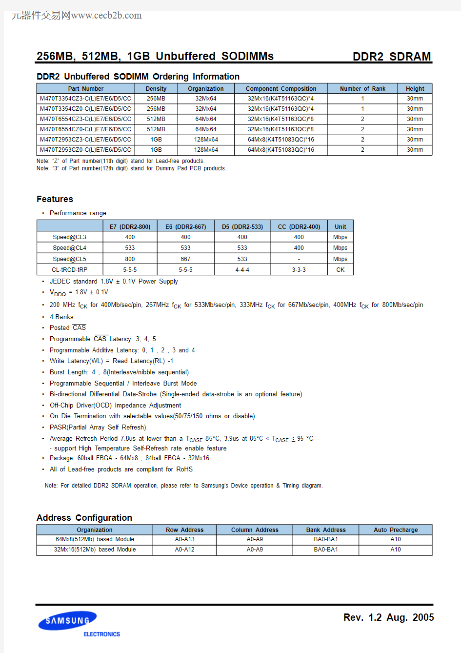
DDR2 Unbuffered SODIMM Ordering Information
Part Number Density Organization Component Composition Number of Rank Height M470T3354CZ3-C(L)E7/E6/D5/CC256MB32Mx6432Mx16(K4T51163QC)*4130mm M470T3354CZ0-C(L)E7/E6/D5/CC256MB32Mx6432Mx16(K4T51163QC)*4130mm M470T6554CZ3-C(L)E7/E6/D5/CC512MB64Mx6432Mx16(K4T51163QC)*8230mm M470T6554CZ0-C(L)E7/E6/D5/CC512MB64Mx6432Mx16(K4T51163QC)*8230mm M470T2953CZ3-C(L)E7/E6/D5/CC1GB128Mx6464Mx8(K4T51083QC)*16230mm M470T2953CZ0-C(L)E7/E6/D5/CC1GB128Mx6464Mx8(K4T51083QC)*16230mm Note: “Z” of Part number(11th digit) stand for Lead-free products.
Note: “3” of Part number(12th digit) stand for Dummy Pad PCB products.
Features
?Performance range
E7 (DDR2-800)E6 (DDR2-667)D5 (DDR2-533)CC (DDR2-400)Unit Speed@CL3400400400400Mbps
Speed@CL4533533533400Mbps
Speed@CL5800667533-Mbps
CL-tRCD-tRP5-5-55-5-54-4-43-3-3CK
?JEDEC standard 1.8V ± 0.1V Power Supply
?V DDQ = 1.8V ± 0.1V
?200 MHz f CK for 400Mb/sec/pin, 267MHz f CK for 533Mb/sec/pin, 333MHz f CK for 667Mb/sec/pin, 400MHz f CK for 800Mb/sec/pin ?4Banks
?Posted CAS
?Programmable CAS Latency: 3, 4, 5
?Programmable Additive Latency: 0, 1 , 2 , 3 and 4
?Write Latency(WL) = Read Latency(RL) -1
?Burst Length: 4 , 8(Interleave/nibble sequential)
?Programmable Sequential / Interleave Burst Mode
?Bi-directional Differential Data-Strobe (Single-ended data-strobe is an optional feature)
?Off-Chip Driver(OCD) Impedance Adjustment
?On Die Termination with selectable values(50/75/150 ohms or disable)
?PASR(Partial Array Self Refresh)
?Average Refresh Period 7.8us at lower than a T CASE 85°C, 3.9us at 85°C < T CASE < 95 °C
- support High Temperature Self-Refresh rate enable feature
?Package: 60ball FBGA - 64Mx8 , 84ball FBGA - 32Mx16
?All of Lead-free products are compliant for RoHS
Note: For detailed DDR2 SDRAM operation, please refer to Samsung’s Device operation & Timing diagram.
Address Configuration
Organization Row Address Column Address Bank Address Auto Precharge 64Mx8(512Mb) based Module A0-A13A0-A9BA0-BA1A10
32Mx16(512Mb) based Module A0-A12A0-A9BA0-BA1A10
Pin Configurations (Front side/Back side)
Note : NC = No Connect; NC, TEST(pin 163)is for bus analysis tool and is not connected on normal memory modules.
Pin
Front
Pin
Back
Pin
Front
Pin
Back
Pin
Front
Pin
Back
Pin
Front
Pin
Back
1V REF 2V SS 51DQS252DM2101A1102A0151DQ42152DQ463V SS 4DQ453V SS 54V SS 103V DD 104V DD 153DQ43154DQ475DQ06DQ555DQ1856DQ22105A10/AP 106BA1155V SS 156V SS 7DQ18V SS 57DQ1958DQ23107BA0108RAS 157DQ48158DQ529V SS 10DM059V SS 60V SS 109WE 110S0159DQ49160DQ5311DQS012V SS 61DQ2462DQ28111V DD 112V DD 161V SS 162V SS 13DQS014DQ663DQ2564DQ29113CAS 114ODT0163NC, TEST 164CK115V SS 16DQ765V SS 66V SS 115NC/S1116A13165V SS 166CK117DQ218V SS 67DM368DQS3117V DD 118V DD 167DQS6168V SS 19DQ320DQ1269NC 70DQS3119NC/ODT1120NC 169DQS6170DM621V SS 22DQ1371V SS 72V SS 121V SS 122V SS 171V SS 172V SS 23DQ824V SS 73DQ2674DQ30123DQ32124DQ36173DQ50174DQ5425DQ926DM175DQ2776DQ31125DQ33126DQ37175DQ51176DQ5527V SS 28V SS 77V SS 78V SS 127V SS 128V SS 177V SS 178V SS 29DQS130CK079CKE080NC/CKE1129DQS4130DM4179DQ56180DQ6031DQS132CK081V DD 82V DD
131DQS4132V SS 181DQ57182DQ6133V SS 34V SS 83NC 84NC 133V SS 134DQ38183V SS 184V SS 35DQ1036DQ1485BA286NC 135DQ34136DQ39185DM7186DQS737DQ1138DQ1587V DD 88V DD 137DQ35138V SS 187V SS 188DQS739V SS 40V SS 89A1290A11139V SS 140DQ44189DQ58190V SS 41V SS 42V SS 91A992A7141DQ40142DQ45191DQ59192DQ6243DQ1644DQ2093A894A6143DQ41144V SS 193V SS 194DQ6345DQ1746DQ2195V DD 96V DD 145V SS 146DQS5195SDA 196V SS 47V SS 48V SS 97A598A4147DM5148DQS5197SCL 198SA049
DQS2
50
NC
99
A3
100
A2
149
V SS
150
V SS
199
V DD SPD
200
SA1
Pin Description
Pin Name Function
Pin Name
Function
CK0,CK1Clock Inputs, positive line SDA SPD Data Input/Output
CK0,CK1Clock Inputs, negative line SA1,SA0SPD address CKE0,CKE1Clock Enables DQ0~DQ63Data Input/Output RAS Row Address Strobe DM0~DM7Data Masks CAS Column Address Strobe DQS0~DQS7Data strobes
WE Write Enable DQS0~DQS7Data strobes complement S0,S1
Chip Selects TEST Logic Analyzer specific test pin (No connect on So-DIMM)A0~A9, A11~A13Address Inputs
V DD Core and I/O Power A10/AP Address Input/Autoprecharge V SS Ground
BA0,BA1SDRAM Bank Address V REF Input/Output Reference ODT0,ODT1On-die termination control
V DD SPD SPD Power
SCL
Serial Presence Detect(SPD) Clock Input
NC
Spare pins, No connect
Input/Output Functional Description
Symbol Type Function
CK0-CK1
CK0-CK1Input The system clock inputs. All address and command lines are sampled on the cross point of the rising edge of CK and fall-ing edge of CK . A Delay Locked Loop (DLL) circuit is driven from the clock input and output timing for read operations is synchronized to the input clock.
CKE0-CKE1Input Activates the DDR2 SDRAM CK signal when high and deactivates the CK signal when low, By deactivating the clocks, CKE low initiates the Power Down mode or the Self Refesh mode.
S0-S1Input Enables the associated DDR2 SDRAM command decoder when low and disables the command decoder when high. When the command decoder is disabled, new commands are ignored but previous operations continue. Rank 0 is selected by S0, Rank 1 is selected by S1. Ranks are also called “Physical banks”.
RAS, CAS, WE Input When sampled at the cross point of the rising edge of CK and falling edge of CK, CAS, RAS, and WE define the operation to be executed by the SDRAM.
BA0~BA1Input Selects which DDR2 SDRAM internal bank is activated.
ODT0~ODT1Input Asserts on-die termination for DQ, DM, DQS, and DQS signals if enabled via the DDR2 SDRAM Extended Mode Register Set (EMRS).
A0~A9, A10/AP, A11~A13Input
During a Bank Activate command cycle, defines the row address when sampled at the cross point of the rising edge of CK and falling edge of CK. During a Read or Write command cycle, defines the column address when sampled at the cross point of the rising edge of CK and falling edge of CK. In addition to the column address, AP is used to invoke autopre-charge operation at the end of the burst read or write cycle. If AP is high, autoprecharge is selected and BA0-BAn defines the bank to be precharged. If AP is low, autoprecharge is disabled. During a Precharge command cycle, AP is used in con-junction with BA0-BAn to control which bank(s) to precharge. If AP is high, all banks will be pecharged regardiess of the state of BA0-BAn inputs. If AP is low, then BA0-BAn are used to define which bank to precharge.
DQ0~DQ63In/Out Data Input/Output pins.
DM0~DM7Input The data write masks, associated with one data byte. In Write mode, DM operates as a byte mask by allowing input data to be written if it is low but blocks the write operation if it is high. In Read mode, DM lines have no effect.
DQS0~DQS7 DQS0~DQS7In/Out
The data strobes, associated with one data byte, sourced with data transfers. In Write mode, the data strobe is sourced by the controller and is centered in the data window. In Read mode, the data strobe is sourced by the DDR2 SDRAMs and is sent at the leading edge of the data window. DQS signals are complements, and timing is relative to the crosspoint of respective DQS and DQS If the module is to be operated in single ended strobe mode, all DQS signals must be tied on the system board to VSS and DDR2 SDRAM mode registers programmed appropriately.
V DD,V DD
SPD,V SS
Supply Power supplies for core, I/O, Serial Presence Detect, and ground for the module.
SDA In/Out This is a bidirectional pin used to transfer data into or out of the SPD EEPROM. A resistor must be connected to V DD to act as a pull up.
SCL Input This signal is used to clock data into and out of the SPD EEPROM. A resistor may be connected from SCL to V DD to act as a pull up.
SA0~SA1Input Address pins used to select the Serial Presence Detect base address.
TEST In/Out The TEST pin is reserved for bus analysis tools and is not connected on normal memory modules(SO-DIMMs).
Functional Block Diagram: 512MB, 64Mx64 Module (Populated as 2 rank of x16 DDR2 SDRAMs)
M470T6554CZ3/M470T6554CZ0
DQS1DQS1DM1
CS DQ8DQ9DQ10DQ11DQ12DQ13DQ14DQ15
I/O 0I/O 1I/O 2I/O 3I/O 4I/O 5I/O 6I/O 7D0LDQS LDQS
LDM
DQS0DQS0DM0
DQ0DQ1DQ2DQ3DQ4DQ5DQ6DQ7
I/O 8I/O 9I/O 10I/O 11I/O 12I/O 13I/O 14I/O 15UDQS UDQS UDM DQS5DQS5DM5
CS DQ40DQ41DQ42DQ43DQ44DQ45DQ46DQ47
I/O 0I/O 1I/O 2I/O 3I/O 4I/O 5I/O 6I/O 7D2LDQS LDQS
LDM
DQS4DQS4DM4
DQ32DQ33DQ34DQ35DQ36DQ37DQ38DQ39
I/O 8I/O 9I/O 10I/O 11I/O 12I/O 13I/O 14I/O 15UDQS UDQS UDM DQS3DQS3DM3
CS DQ24DQ25DQ26DQ27DQ28DQ29DQ30DQ31
I/O 0I/O 1I/O 2I/O 3I/O 4I/O 5I/O 6I/O 7D1LDQS LDQS
LDM
DQS2DQS2DM2
DQ16DQ17DQ18DQ19DQ20DQ21DQ22DQ23
I/O 8I/O 9I/O 10I/O 11I/O 12I/O 13I/O 14I/O 15
UDQS UDQS UDM DQS7DQS7DM7
CS DQ56DQ57DQ58DQ59DQ60DQ61DQ62DQ63
I/O 0I/O 1I/O 2I/O 3I/O 4I/O 5I/O 6I/O 7D3LDQS LDQS
LDM
I/O 8I/O 9I/O 10I/O 11I/O 12I/O 13I/O 14I/O 15
UDQS UDQS UDM C
K E O D T
C
K E O D T C
K E O D T
C
K E O D T CS I/O 0I/O 1I/O 2I/O 3I/O 4I/O 5I/O 6I/O 7D4LDQS LDQS
LDM
I/O 8I/O 9I/O 10I/O 11I/O 12I/O 13I/O 14I/O 15UDQS UDQS UDM CS I/O 0I/O 1I/O 2I/O 3I/O 4I/O 5I/O 6I/O 7D5LDQS LDQS
LDM
I/O 8I/O 9I/O 10I/O 11I/O 12I/O 13I/O 14I/O 15
UDQS UDQS UDM C
K E O D T
C
K E O D T
CS I/O 0I/O 1I/O 2I/O 3I/O 4I/O 5I/O 6I/O 7D6LDQS LDQS
LDM
I/O 8I/O 9I/O 10I/O 11I/O 12I/O 13I/O 14I/O 15UDQS UDQS UDM CS I/O 0I/O 1I/O 2I/O 3I/O 4I/O 5I/O 6I/O 7D7LDQS LDQS
LDM
I/O 8I/O 9I/O 10I/O 11I/O 12I/O 13I/O 14I/O 15
UDQS UDQS UDM C
K E O D T
C
K E O D T
CKE0CKE1ODT0ODT1V SS
DDR2 SDRAMs D0 - D7, SPD
V REF DDR2 SDRAMs D0 - D7
DDR2 SDRAMs D0 - D7, V DD and V DD Q V DD V DD SPD Serial PD
A0 - A13
DDR2 SDRAMs D0 - D7RAS DDR2 SDRAMs D0 - D7CAS DDR2 SDRAMs D0 - D7WE
DDR2 SDRAMs D0 - D7
BA0 - BA1DDR2 SDRAMs D0 - D7 + 5%
Notes :
1. DQ,DM, DQS/DQS resistors : 22 Ohms ± 5%.
2. BAx, Ax, RAS, CAS, WE resistors :
3.0 Ohms ± 5%.
* Wire per Clock Loading Table/Wiring Diagrams
* Clock Wiring
Clock Input DDR2 SDRAMs *CK0/CK0*CK1/CK1
4 DDR2 SDRAMs 4 DDR2 SDRAMs
3? + 5%
DQS6DQS6DM6
DQ48DQ49DQ50DQ51DQ52DQ53DQ54DQ55
Functional Block Diagram: 256MB, 32Mx64 Module (Populated as 1 rank of x16 DDR2 SDRAMs)
M470T3354CZ3/M470T3354CZ0
DQS1DQS1DM1
CS DQ8DQ9DQ10DQ11DQ12DQ13DQ14DQ15
I/O 0I/O 1I/O 2I/O 3I/O 4I/O 5I/O 6I/O 7D0LDQS LDQS
LDM
DQS0DQS0DM0
DQ0DQ1DQ2DQ3DQ4DQ5DQ6DQ7
I/O 8I/O 9I/O 10I/O 11I/O 12I/O 13I/O 14I/O 15UDQS UDQS UDM DQS5DQS5DM5
CS DQ40DQ41DQ42DQ43DQ44DQ45DQ46DQ47
I/O 0I/O 1I/O 2I/O 3I/O 4I/O 5I/O 6I/O 7D2LDQS LDQS
LDM
DQS4DQS4DM4
DQ32DQ33DQ34DQ35DQ36DQ37DQ38DQ39
I/O 8I/O 9I/O 10I/O 11I/O 12I/O 13I/O 14I/O 15UDQS UDQS UDM DQS3DQS3DM3
CS DQ24DQ25DQ26DQ27DQ28DQ29DQ30DQ31
I/O 0I/O 1I/O 2I/O 3I/O 4I/O 5I/O 6I/O 7D1LDQS LDQS
LDM
DQS2DQS2DM2
DQ16DQ17DQ18DQ19DQ20DQ21DQ22DQ23
I/O 8I/O 9I/O 10I/O 11I/O 12I/O 13I/O 14I/O 15
UDQS UDQS UDM DQS7DQS7DM7
CS DQ56DQ57DQ58DQ59DQ60DQ61DQ62DQ63
I/O 0I/O 1I/O 2I/O 3I/O 4I/O 5I/O 6I/O 7D3LDQS LDQS
LDM
DQS6DQS6DM6
DQ48DQ49DQ50DQ51DQ52DQ53DQ54DQ55
I/O 8I/O 9I/O 10I/O 11I/O 12I/O 13I/O 14I/O 15
UDQS UDQS UDM O
D T C K E
O
D T C K E
O
D T C K E
O
D T C K E
ODT0CKE0V SS
DDR2 SDRAMs D0 - D3, SPD
V REF DDR2 SDRAMs D0 - D3
DDR2 SDRAMs D0 - D3, V DD and V DD Q V DD V DD SPD Serial PD
DDR2 SDRAMs D0 - D3DDR2 SDRAMs D0 - D3DDR2 SDRAMs D0 - D3DDR2 SDRAMs D0 - D3
DDR2 SDRAMs D0 - D3Notes :
1. DQ,DM, DQS/DQS resistors : 22 Ohms ± 5%.
2. BAx, Ax, RAS, CAS, WE resistors :
3.0 Ohms ± 5%.
* Wire per Clock Loading Table/Wiring Diagrams
* Clock Wiring
Clock Input DDR2 SDRAMs *CK0/CK0*CK1/CK1
2 DDR2 SDRAMs 2 DDR2 SDRAMs
3? + 5%
Functional Block Diagram: 1GB, 128Mx64 Module (Populated as 2 ranks of x8 DDR2 SDRAMs)
M470T2953CZ3/M470T2953CZ0
ODT0CKE0S1ODT1CKE1V SS
DDR2 SDRAMs D0 - D15, SPD
V REF DDR2 SDRAMs D0 - D15
DDR2 SDRAMs D0 - D15, V DD and V DD Q V DD V DD SPD Serial PD
A0 - A13
DDR2 SDRAMs D0 - D15DDR2 SDRAMs D0 - D15DDR2 SDRAMs D0 - D15DDR2 SDRAMs D0 - D15
BA0 - BA1DDR2 SDRAMs D0 - D1510 + 5%
10? + 5%
DQS1DQS1DM1
CS0DQ8DQ9DQ10DQ11DQ12DQ13DQ14DQ15
I/O 0I/O 1I/O 2I/O 3I/O 4I/O 5I/O 6I/O 7
D0
DQS DQS DM DQS0DQS0DM0
DQ0DQ1DQ2DQ3DQ4DQ5DQ6DQ7
I/O 8
I/O 9I/O 10I/O 11I/O 12I/O 13I/O 14I/O 15
DQS
DQS DM DQS5DQS5DM5
DQ40DQ41DQ42DQ43DQ44DQ45DQ46DQ47
I/O 0I/O 1I/O 2I/O 3I/O 4I/O 5I/O 6I/O 7
D4
DQS DQS DM DQS4DQS4DM4
DQ32DQ33DQ34DQ35DQ36DQ37DQ38DQ39
I/O 8I/O 9I/O 10I/O 11I/O 12I/O 13I/O 14I/O 15
DQS DQS DM DQS3DQS3DM3
DQ24DQ25DQ26DQ27DQ28DQ29DQ30DQ31
I/O 0I/O 1I/O 2I/O 3I/O 4I/O 5I/O 6I/O 7
DQS DQS DM DQS2DQS2DM2
DQ16DQ17DQ18DQ19DQ20DQ21DQ22DQ23
I/O 8
I/O 9I/O 10I/O 11I/O 12I/O 13I/O 14I/O 15
DQS
DQS
DM
DQS7DQS7DM7
DQ56DQ57DQ58DQ59DQ60DQ61DQ62DQ63
I/O 0I/O 1I/O 2I/O 3I/O 4I/O 5I/O 6I/O 7
DQS DQS DM DQS6DQS6DM6
DQ48DQ49DQ50DQ51DQ52DQ53DQ54DQ55
I/O 8I/O 9I/O 10I/O 11I/O 12I/O 13I/O 14I/O 15
DQS DQS DM O
D T 0
C K E 0
CS 1I/O 0I/O 1I/O 2I/O 3I/O 4I/O 5I/O 6I/O 7
D8
DQS DQS DM I/O 8
I/O 9I/O 10I/O 11I/O 12I/O 13I/O 14I/O 15
DQS
DQS DM I/O 0I/O 1I/O 2I/O 3I/O 4I/O 5I/O 6I/O 7
DQS DQS DM I/O 8
I/O 9I/O 10I/O 11I/O 12I/O 13I/O 14I/O 15
DQS
DQS
DM
O
D T 1
C K E 1
I/O 0I/O 1I/O 2I/O 3I/O 4I/O 5I/O 6I/O 7
D12
DQS DQS DM I/O 8I/O 9I/O 10I/O 11I/O 12I/O 13I/O 14I/O 15
DQS DQS DM I/O 0I/O 1I/O 2I/O 3I/O 4I/O 5I/O 6I/O 7
DQS DQS DM I/O 8I/O 9I/O 10I/O 11I/O 12I/O 13I/O 14I/O 15
DQS DQS DM CS0O
D T 0C K
E 0
CS 1O
D T 1
C K E 1
CS0D1D5
O D T
0C K E 0
CS 1D9O D T
1C K E 1
D13
CS0O
D T 0C K
E 0
CS 1O
D T 1
C K E 1
CS0D2
D6
O
D T 0C K
E 0
CS 1D10
O
D T 1
C K E 1
D14
CS0O
D T 0C K
E 0
CS 1O
D T 1
C K E 1
CS0D3D7
O D T 0C K E 0
CS 1D11O D T 1C K E 1
D15
CS0O
D T 0C K
E 0
CS 1O
D T 1
C K E 1
Notes :
1. DQ,DM, DQS/DQS resistors : 22 Ohms ± 5%.
2. BAx, Ax, RAS, CAS, WE resistors :
3.0 Ohms ± 5%.
* Wire per Clock Loading Table/Wiring Diagrams
* Clock Wiring
Clock Input
DDR2 SDRAMs *CK0/CK0*CK1/CK1
8 DDR2 SDRAMs 8 DDR2 SDRAMs
Absolute Maximum DC Ratings
Note :
1. Stresses greater than those listed under “Absolute Maximum Ratings” may cause permanent damage to the device. This is a stress rating only and functional operation of the device at these or any other conditions above those indicated in the operational sections of this specification is not implied. Exposure to absolute maximum rating conditions for extended periods may affect reliability.
2. Storage Temperature is the case surface temperature on the center/top side of the DRAM. For the measurement conditions, please refer to JESD51-2 standard.
AC & DC Operating Conditions
Recommended DC Operating Conditions (SSTL - 1.8)
Note : There is no specific device V DD supply voltage requirement for SSTL-1.8 compliance. However under all conditions V DDQ must be less than or equal
to V DD .
1. The value of V REF may be selected by the user to provide optimum noise margin in the system. Typically the value of V REF is expected to be about 0.5 x V DDQ of the transmitting device and V REF is expected to track variations in V DDQ .
2. Peak to peak AC noise on V REF may not exceed +/-2% V REF (DC).
3. V TT of transmitting device must track V REF of receiving device.
4. AC parameters are measured with V DD , V DDQ and V DDL tied together.
Symbol Parameter
Rating Units Notes V DD Voltage on V DD pin relative to V SS - 1.0 V ~ 2.3 V V 1V DDQ Voltage on V DDQ pin relative to V SS - 0.5 V ~ 2.3 V V 1V DDL Voltage on V DDL pin relative to V SS - 0.5 V ~ 2.3 V V 1V IN, V OUT Voltage on any pin relative to V SS - 0.5 V ~ 2.3 V V
1
T STG
Storage Temperature
-55 to +100
°C 1, 2
Symbol Parameter
Rating
Units Notes
Min.Typ. Max.V DD Supply Voltage 1.7 1.8 1.9V V DDL Supply Voltage for DLL 1.7 1.8 1.9V 4V DDQ Supply Voltage for Output 1.7 1.8 1.9V 4V REF Input Reference Voltage 0.49*V DDQ 0.50*V DDQ
0.51*V DDQ mV 1,2V TT
Termination Voltage
V REF -0.04
V REF
V REF +0.04
V
3
V DDQ V IH (AC) min
V IH (DC) min V REF
V IL (DC) max V IL (AC) max
V SS
< AC Input Test Signal Waveform >
V SWING(MAX)
delta TR
delta TF
V REF - V IL (AC) max
delta TF
Falling Slew =
Rising Slew =
V IH (AC) min - V REF
delta TR
Operating Temperature Condition
1.Operating Temperature is the case surface temperature on the center/top side of the DRAM. For the measurement conditions, please refer to
JESD51.2 standard.
2.At 85 - 95 °C operation temperature range, doubling refresh commands in frequency to a 32ms period ( tREFI=
3.9 us ) is required, and to enter to self refresh mode at this temperature range, an EMRS command is required to change internal refresh rate.
Input DC Logic Level
Input AC Logic Level
AC Input Test Conditions
Notes:
1. Input waveform timing is referenced to the input signal crossing through the V IH/IL (AC) level applied to the device under test.
2. The input signal minimum slew rate is to be maintained over the range from V REF to V IH (AC) min for rising edges and the range from V REF to V IL (AC)max for falling edges as shown in the below figure.
3. AC timings are referenced with input waveforms switching from V IL (AC) to V IH (AC) on the positive transitions and V IH (AC) to V IL (AC) on the negative transitions.
Symbol Parameter Rating Units
Notes
TOPER
Operating Temperature
0 to 95
°C 1, 2, 3
Symbol Parameter Min.Max.Units Notes
V IH (DC)DC input logic high V REF + 0.125
V DDQ + 0.3V V IL (DC)
DC input logic low
- 0.3
V REF - 0.125
V
Symbol Parameter DDR2-400, DDR2-533DDR2-667, DDR2-800Units Min.Max.Min.Max.
V IH (ac)ac input logic high V REF + 0.250
-V REF + 0.200
V V IL (ac)
ac input logic low
-V REF - 0.250
V REF - 0.200
V
Symbol Condition
Value Units Notes V REF Input reference voltage
0.5 * V DDQ
V 1V SWING(MAX)
Input signal maximum peak to peak swing 1.0V 1SLEW
Input signal minimum slew rate
1.0
V/ns
2, 3
IDD Specification Parameters Definition
(IDD values are for full operating range of Voltage and Temperature)
Symbol Proposed Conditions Units Notes
IDD0Operating one bank active-precharge current;
t CK = t CK(IDD), t RC = t RC(IDD), t RAS = t RASmin(IDD); CKE is HIGH, CS\ is HIGH between valid commands;
Address bus inputs are SWITCHING; Data bus inputs are SWITCHING
mA
IDD1Operating one bank active-read-precharge current;
IOUT = 0mA; BL = 4, CL = CL(IDD), AL = 0; t CK = t CK(IDD), t RC = t RC (IDD), t RAS = t RASmin(IDD), t RCD =
t RCD(IDD); CKE is HIGH, CS\ is HIGH between valid commands; Address bus inputs are SWITCHING; Data pattern
is same as IDD4W
mA
IDD2P Precharge power-down current;
All banks idle; t CK = t CK(IDD); CKE is LOW; Other control and address bus inputs are STABLE; Data bus inputs are FLOATING
mA
IDD2Q Precharge quiet standby current;
All banks idle; t CK = t CK(IDD); CKE is HIGH, CS\ is HIGH; Other control and address bus inputs are STABLE; Data
bus inputs are FLOATING
mA
IDD2N Precharge standby current;
All banks idle; t CK = t CK(IDD); CKE is HIGH, CS\ is HIGH; Other control and address bus inputs are SWITCHING;
Data bus inputs are SWITCHING
mA
IDD3P Active power-down current;
All banks open; t CK = t CK(IDD); CKE is LOW; Other control and address bus
inputs are STABLE; Data bus inputs are FLOATING
Fast PDN Exit MRS(12) = 0mA mA
Slow PDN Exit MRS(12) = 1mA mA
IDD3N Active standby current;
All banks open; t CK = t CK(IDD), t RAS = t RASmax(IDD), t RP = t RP(IDD); CKE is HIGH, CS\ is HIGH between valid commands; Other control and address bus inputs are SWITCHING; Data bus inputs are SWITCHING
mA
IDD4W Operating burst write current;
All banks open, Continuous burst writes; BL = 4, CL = CL(IDD), AL = 0; t CK = t CK(IDD), t RAS = t RASmax(IDD), t RP
= t RP(IDD); CKE is HIGH, CS\ is HIGH between valid commands; Address bus inputs are SWITCHING; Data bus
inputs are SWITCHING
mA
IDD4R Operating burst read current;
All banks open, Continuous burst reads, IOUT = 0mA; BL = 4, CL = CL(IDD), AL = 0; t CK = t CK(IDD), t RAS = t RAS-
max(IDD), t RP = t RP(IDD); CKE is HIGH, CS\ is HIGH between valid commands; Address bus inputs are SWITCH-
ING; Data pattern is same as IDD4W
mA
IDD5B Burst auto refresh current;
t CK = t CK(IDD); Refresh command at every t RFC(IDD) interval; CKE is HIGH, CS\ is HIGH between valid commands;
Other control and address bus inputs are SWITCHING; Data bus inputs are SWITCHING
mA
IDD6Self refresh current;
CK and CK\ at 0V; CKE ≤ 0.2V; Other control and address bus inputs are
FLOATING; Data bus inputs are FLOATING
Normal mA
Low Power mA
IDD7Operating bank interleave read current;
All bank interleaving reads, IOUT = 0mA; BL = 4, CL = CL(IDD), AL = t RCD(IDD)-1*t CK(IDD); t CK = t CK(IDD), t RC =
t RC(IDD), t RRD = t RRD(IDD), t FAW = t FAW(IDD), t RCD = 1*t CK(IDD); CKE is HIGH, CS\ is HIGH between valid commands; Address bus inputs are STABLE during DESELECTs; Data pattern is same as IDD4R; Refer to the follow-
ing page for detailed timing conditions
mA
Operating Current Table(1-1) (T A =0o C, VDD= 1.9V)
M470T6554CZ3/M470T6554CZ0 : 64Mx64 512MB Module
* Module IDD was calculated on the basis of component IDD and can be differently measured according to DQ loading cap.
Symbol 800@CL=5667@CL=5533@CL=4400@CL=3Unit Notes
CE7
LE7
CE6LE6CD5LD5CCC LCC IDD0TBD 560480520460520460mA IDD1TBD 620540580520580520mA IDD2P TBD 644064366436mA IDD2Q TBD 280240240200240200mA IDD2N TBD 320280280240280240mA IDD3P-F TBD 240200240200240200mA IDD3P-S TBD 966496649664mA IDD3N TBD 380320340280340280mA IDD4W TBD 860800760700680620mA IDD4R TBD 880820780720700640mA IDD5TBD 760680700620700620mA IDD6TBD 643264326432mA IDD7
TBD
1,360
1,220
1,340
1,200
1,340
1,200
mA
M470T3354CZ3/M470T3354CZ0 : 32Mx64 256MB Module
* Module IDD was calculated on the basis of component IDD and can be differently measured according to DQ loading cap.
Symbol 800@CL=5667@CL=5533@CL=4400@CL=3Unit Notes
CE7
LE7
CE6LE6CD5LD5CCC LCC IDD0TBD 400340380340380340mA IDD1TBD 460400440400440400mA IDD2P TBD 322032183218mA IDD2Q TBD 140120120100120100mA IDD2N TBD 160140140120140120mA IDD3P-F TBD 120100120100120100mA IDD3P-S TBD 483248324832mA IDD3N TBD 220180200160200160mA IDD4W TBD 700660620580540500mA IDD4R TBD 720680640600560520mA IDD5TBD 600540560500560500mA IDD6TBD 321632163216mA IDD7
TBD
1,200
1,080
1,200
1,080
1,200
1,080
mA
Operating Current Table(1-2) (T A =0o C, VDD= 1.9V)
M470T2953CZ3/M470T2953CZ0 : 128Mx64 1GB Module
* Module IDD was calculated on the basis of component IDD and can be differently measured according to DQ loading cap.
Symbol 800@CL=5667@CL=5533@CL=4400@CL=3Unit Notes
CE7
LE7
CE6LE6CD5LD5CCC LCC IDD0TBD 1,000800920760920760mA IDD1TBD 1,1208801,0408401,040840mA IDD2P TBD 128801287212872mA IDD2Q TBD 560480480400480400mA IDD2N TBD 640560560480560480mA IDD3P-F TBD 480400480400480400mA IDD3P-S TBD 192128192128192128mA IDD3N TBD 760640680560680560mA IDD4W TBD 1,4401,3201,2401,1201,1601,000mA IDD4R TBD 1,4801,3601,2801,1601,1601,040mA IDD5TBD 1,5201,3601,4001,2401,4001,240mA IDD6TBD 128641286412864mA IDD7
TBD
2,080
1,720
2,040
1,680
2,040
1,680
mA
Input/Output Capacitance (VDD=1.8V, VDDQ=1.8V, TA=25o C)
* DM is internally loaded to match DQ and DQS identically.
Parameter Symbol
Min
Max
Min
Max
Min
Max
Units
Non-ECC
M470T6554CZ3M470T6554CZ0M470T3354CZ3M470T3354CZ0M470T2953CZ3M470T2953CZ0Input capacitance, CK and CK
CCK -32-24-48pF
Input capacitance, CKE , CS, Addr, RAS, CAS, WE CI
-34-34-42Input/output capacitance, DQ, DM, DQS, DQS
CIO(400/533)-10-6-10CIO(667/800)
-9
- 5.5
-9
Electrical Characteristics & AC Timing for DDR2-800/667/533/400
(0 °C < T OPER < 95 °C; V DDQ = 1.8V + 0.1V; V DD = 1.8V + 0.1V)
Refresh Parameters by Device Density
Speed Bins and CL, tRCD, tRP, tRC and tRAS for Corresponding Bin
Timing Parameters by Speed Grade
(Refer to notes for informations related to this table at the bottom)
Parameter
Symbol
256Mb 512Mb 1Gb 2Gb 4Gb Units Refresh to active/Refresh command time tRFC 75105127.5195327.5ns Average periodic refresh interval
tREFI
0 °C ≤ T CASE ≤ 85°C 7.87.87.87.87.8μs 85 °C < T CASE ≤ 95°C 3.9
3.9
3.9
3.9
3.9
μs
Speed
DDR2-800(E7)
DDR2-667(E6)
DDR2-533(D5)
DDR2-400(CC)
Units
Bin (CL - tRCD - tRP) 5 - 5 - 5
5 - 5 - 5 4 - 4 - 4
3 - 3 - 3
Parameter min max min max min max min max tCK, CL=358585858ns tCK, CL=4 3.758 3.758 3.75858ns tCK, CL=5 2.5838
3.758
--ns tRCD 12.5-151515ns tRP 12.5-151515ns tRC 51.5-545555
ns
tRAS
39
70000
39
70000
40
70000
4070000
ns
Parameter
Symbol
DDR2-800DDR2-667DDR2-533DDR2-400Units Notes
min
max
min
max
min
max
min
max
DQ output access time from CK/CK tAC - 400400-450+450-500+500-600+600ps DQS output access time from CK/CK tDQSCK - 350350-400+400-450+450-500+500ps CK high-level width tCH 0.450.550.450.550.450.550.450.55tCK CK low-level width tCL 0.450.550.450.550.450.550.450.55tCK CK half period tHP min(tCL,t CH)x min(tCL, tCH)x min(tCL, tCH)x min(tCL, tCH)x ps Clock cycle time, CL=x tCK 25008000300080003750800050008000ps DQ and DM input hold time tDH(base)125x 175x 225x 275x ps DQ and DM input setup time
tDS(base)50x 100x 100x 150x ps Control & Address input pulse width for each input
tIPW 0.6x 0.6x 0.6x 0.6x tCK DQ and DM input pulse width for each input tDIPW 0.35x 0.35x 0.35x 0.35x tCK Data-out high-impedance time from CK/CK tHZ x tAC max x tAC max x tAC max x tAC max ps DQS low-impedance time from CK/CK tLZ(DQS)tAC min tAC max tAC min tAC max
tAC min
tAC max
tAC min
tAC max ps DQ low-impedance time from CK/CK tLZ(DQ)2*tAC min tAC max 2*tAC min tAC max 2*tACmin tAC max 2*tACmin tAC max ps DQS-DQ skew for DQS and associated DQ signals
tDQSQ x 200x 240x 300x 350ps DQ hold skew factor
tQHS x 300x 340x 400x 450ps DQ/DQS output hold time from DQS
tQH
tHP - tQHS x tHP - tQHS x tHP - tQHS x tHP - tQHS x ps Write command to first DQS latching transition tDQSS - 0.250.25-0.250.25-0.250.25-0.250.25tCK DQS input high pulse width
tDQSH
0.35
x
0.35
x
0.35
x
0.35
x
tCK
Parameter Symbol
DDR2-800DDR2-667DDR2-533DDR2-400
Units Notes min max min max min max min max
DQS input low pulse width tDQSL0.35x0.35x0.35x0.35x tCK DQS falling edge to CK setup time tDSS0.2x0.2x0.2x0.2x tCK DQS falling edge hold time from CK tDSH0.2x0.2x0.2x0.2x tCK Mode register set command cycle time tMRD2x2x2x2x tCK Write postamble tWPST0.40.60.40.60.40.60.40.6tCK Write preamble tWPRE0.35x0.35x0.35x0.35x tCK Address and control input hold time tIH(base)250x275x375x475x ps Address and control input setup time tIS(base)175x200x250x350x ps Read preamble tRPRE0.9 1.10.9 1.10.9 1.10.9 1.1tCK Read postamble tRPST0.40.60.40.60.40.60.40.6tCK Active to active command period for 1KB page
size products
tRRD7.5x7.5x7.5x7.5x ns
Active to active command period for 2KB page
size products
tRRD10x10x10x10x ns
Four Activate Window for 1KB page size
products
tFAW3537.537.537.5ns
Four Activate Window for 2KB page size
products
tFAW45505050ns CAS to CAS command delay tCCD2x222tCK Write recovery time tWR15x15x15x15x ns Auto precharge write recovery + precharge
time
tDAL WR+tRP x WR+tRP x WR+tRP x WR+tRP x tCK Internal write to read command delay tWTR7.57.5x7.5x10x ns Internal read to precharge command delay tRTP7.57.57.57.5ns Exit self refresh to a non-read command tXSNR tRFC + 10tRFC + 10tRFC + 10tRFC + 10ns Exit self refresh to a read command tXSRD200x200200200tCK Exit precharge power down to any non-read
command
tXP2x2x2x2x tCK Exit active power down to read command tXARD2x2x2x2x tCK Exit active power down to read command
(slow exit, lower power)
tXARDS8 - AL7 - AL 6 - AL 6 - AL tCK
CKE minimum pulse width
(high and low pulse width)
tCKE3333tCK
ODT turn-on delay tAOND22222222tCK
ODT turn-on tAON tAC(min)tAC(max)
+ 0.7
tAC(min)
tAC(max)
+0.7
tAC(min)
tAC(max)
+1
tAC(min)
tAC(max)
+1
ns
ODT turn-on(Power-Down mode)tAONPD tAC(min)+
2
2tCK +
tAC(max)
+1
tAC(min)+
2
2tCK+tAC
(max)+1
tAC(min)+
2
2tCK+tA
C(max)+
1
tAC(min)+
2
2tCK+tAC
(max)+1
ns
ODT turn-off delay tAOFD 2.5 2.5 2.5 2.5 2.5 2.5 2.5 2.5tCK
ODT turn-off tAOF tAC(min)tAC(max)
+ 0.6
tAC(min)
tAC(max)
+ 0.6tAC(min)
tAC(max)+
0.6
tAC(min)tAC(max)+
0.6
ns
ODT turn-off (Power-Down mode)tAOFPD tAC(min)+
2
2.5tCK +
tAC(max)
+1
tAC(min)+
2
2.5tCK+
tAC(max)
+1
tAC(min)+
2
2.5tCK+
tAC(max)
+1
tAC(min)+
2
2.5tCK+
tAC(max)
+1
ns
ODT to power down entry latency tANPD3333tCK ODT power down exit latency tAXPD8888tCK OCD drive mode output delay tOIT012012012012ns
Minimum time clocks remains ON after CKE asynchronously drops LOW tDelay
tIS+tCK
+tIH
tIS+tCK
+tIH
tIS+tCK
+tIH
tIS+tCK
+tIH
ns
Physical Dimensions: 32Mbx16 based 64Mx64 Module(2 Rank)
The used device is 32M x16 DDR2 SDRAM, FBGA.DDR2 SDRAM Part NO : K4T51163QC
M470T6554CZ3/M470T6554CZ0
67.60 ± 0.15 mm
4.00 ± 0.1020.00 ± 0.15 m m
30.00 ± 0.15 m m
1
199
11.40 ± 0.15 mm 47.40 ± 0.15 mm
6.00 ± 0.15 m m
Max
Max
a 63.00 ± 0.15 mm
16.25 ± 0.15 mm
min 2.00
FRONT SIDE 4.20 ± 0.15
1.80 ± 0.10
4.00 ± 0.10
1.0 ± 0.05
2.40 ± 0.10
BACK SIDE
0.60 ± 0.150.45 ± 0.03
2.55 ± 0.15
0.20 ± 0.15
DETAIL a DETAIL b
b
Physical Dimensions: 32Mbx16 based 32Mx64 Module(1 Rank)
The used device is 32M x16 DDR2 SDRAM, FBGA.DDR2 SDRAM Part NO : K4T51163QC
M470T3354CZ3/M470T3354CZ0
2.45 mm Max
1.1 mm Max
67.60 ± 0.15 mm
4.00 ± 0.10
20.00 ± 0.15 m m
30.00 ± 0.15 m m
1
199
11.40 ± 0.15 mm 47.40 ± 0.15 mm
6.00 ± 0.15 m m
S P D
a 63.00 ± 0.15 mm
16.25 ± 0.15 mm
min 2.00
b
FRONT SIDE 4.20 ± 0.15
1.80 ± 0.10
4.00 ± 0.10
1.0 ± 0.05
2.40 ± 0.10
BACK SIDE
0.60 ± 0.150.45 ± 0.03
2.55 ± 0.15
0.20 ± 0.15
DETAIL a DETAIL b
Physical Dimensions: 64Mbx8 based 128Mx64 Module(2 Ranks)
M470T2953CZ3/M470T2953CZ0
The used device is 64M x8 DDR2 SDRAM, FBGA.DDR2 SDRAM Part NO : K4T51083QC
3.8 mm 1.1mm max
max
67.60 ± 0.15 mm
4.00 ± 0.1020.00 ± 0.15 m m
30.00 ± 0.15 m
m
1
199
11.40 ± 0.15 mm 47.40 ± 0.15 mm
6.00 ± 0.15 m m
63.00 ± 0.15 mm
16.25 ± 0.15 mm
min 2.00
SPD
a
b
FRONT SIDE 4.20 ± 0.15
1.80 ± 0.10
4.00 ± 0.10
1.0 ± 0.05
2.40 ± 0.10
BACK SIDE
0.60 ± 0.150.45 ± 0.03
2.55 ± 0.15
0.20 ± 0.15
DETAIL a DETAIL b
Revision History
Revision 1.0 (Mar. 2005)
- Initial Release
Revision 1.1 (Mar. 2005)
- Changed IDD0/IDD3N/IDD3P current values. - Added Lowpower current values. Revision 1.2 (Aug. 2005)
- Changed the IDD Current Values.