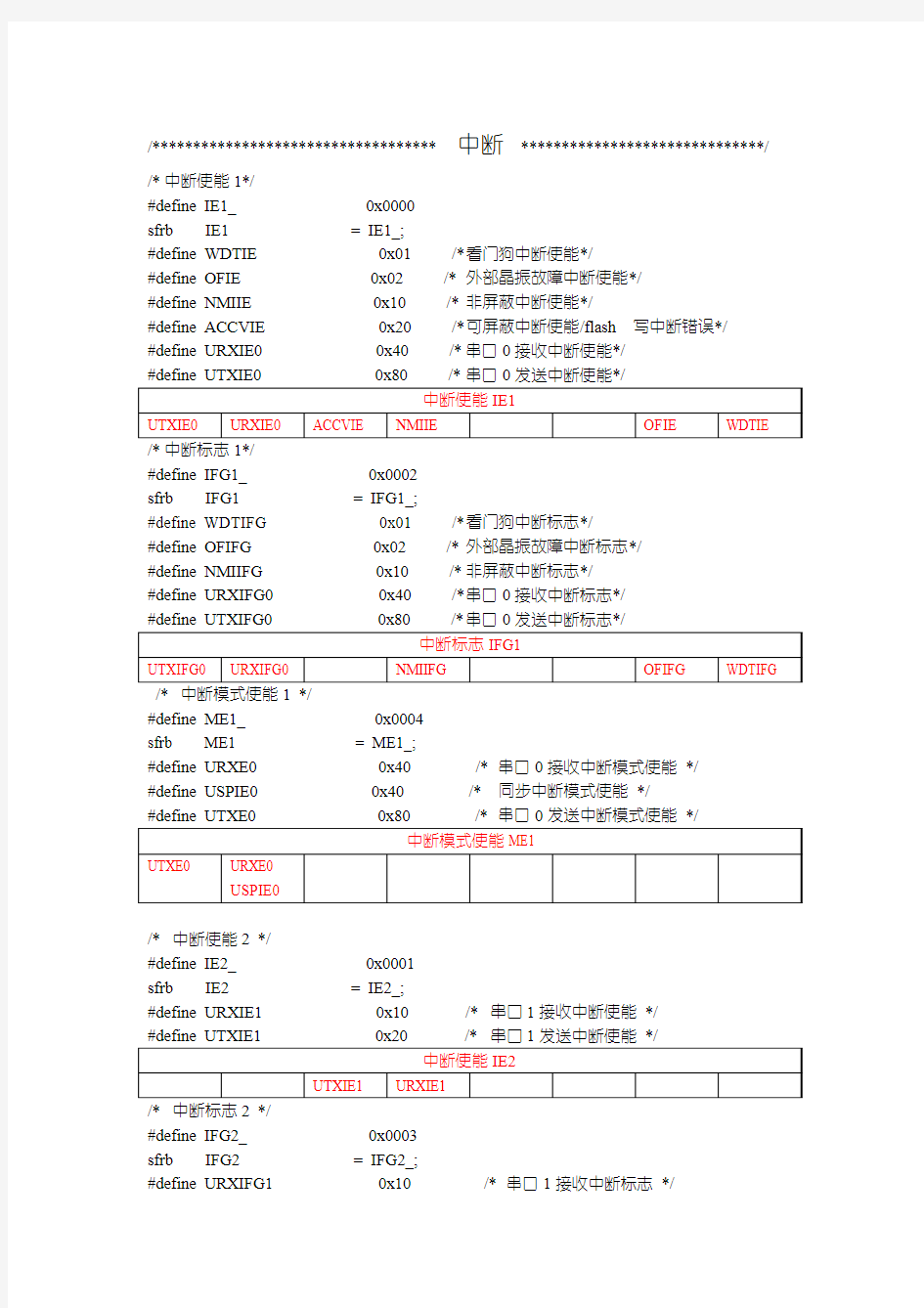
/*********************************** 中断 ******************************/ /*中断使能1*/
#define IE1_ 0x0000
sfrb IE1 = IE1_;
#define WDTIE 0x01 /*看门狗中断使能*/
#define OFIE 0x02 /*外部晶振故障中断使能*/
#define NMIIE 0x10 /*非屏蔽中断使能*/
#define ACCVIE 0x20 /*可屏蔽中断使能/flash写中断错误*/
#define URXIE0 0x40 /*串口0接收中断使能*/
#define UTXIE0 0x80 /*串口0发送中断使能*/
中断使能IE1
UTXIE0 URXIE0 ACCVIE NMIIE OFIE WDTIE /*中断标志1*/
#define IFG1_ 0x0002
sfrb IFG1 = IFG1_;
#define WDTIFG 0x01 /*看门狗中断标志*/
#define OFIFG 0x02 /*外部晶振故障中断标志*/
#define NMIIFG 0x10 /*非屏蔽中断标志*/
#define URXIFG0 0x40 /*串口0接收中断标志*/
#define UTXIFG0 0x80 /*串口0发送中断标志*/
中断标志IFG1
UTXIFG0 URXIFG0 NMIIFG OFIFG WDTIFG /* 中断模式使能1 */
#define ME1_ 0x0004
sfrb ME1 = ME1_;
#define URXE0 0x40 /* 串口0接收中断模式使能 */
#define USPIE0 0x40 /* 同步中断模式使能 */
#define UTXE0 0x80 /* 串口0发送中断模式使能 */
中断模式使能ME1
UTXE0 URXE0
USPIE0
/* 中断使能2 */
#define IE2_ 0x0001
sfrb IE2 = IE2_;
#define URXIE1 0x10 /* 串口1接收中断使能 */
#define UTXIE1 0x20 /* 串口1发送中断使能 */
中断使能IE2
UTXIE1 URXIE1
/* 中断标志2 */
#define IFG2_ 0x0003
sfrb IFG2 = IFG2_;
#define URXIFG1 0x10 /* 串口1接收中断标志 */
#define UTXIFG1 0x20 /* 串口1发送中断标志 */
中断标志IFG2
UTXIFG1 URXIFG1
/* 中断模式使能2 */
#define ME2_ 0x0005
sfrb ME2 = ME2_;
#define URXE1 0x10 /* 串口1接收中断模式使能 */
#define USPIE1 0x10 /* 同步中断模式使能 */
#define UTXE1 0x20 /* 串口1发送中断模式使能 */
中断模式使能ME2
UTXE1 URXE1
USPIE1
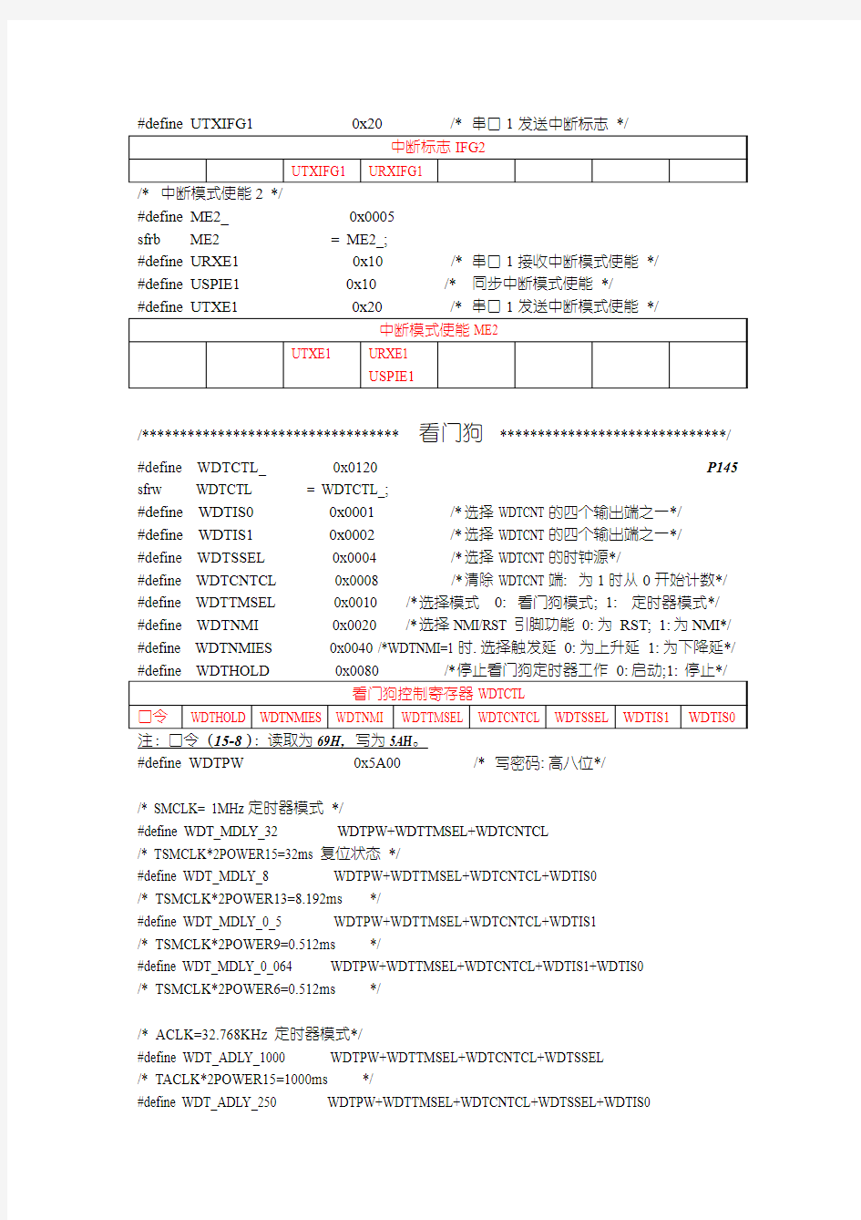
/********************************** 看门狗 ******************************/ #define WDTCTL_ 0x0120 P145 sfrw WDTCTL = WDTCTL_;
#define WDTIS0 0x0001 /*选择WDTCNT的四个输出端之一*/
#define WDTIS1 0x0002 /*选择WDTCNT的四个输出端之一*/
#define WDTSSEL 0x0004 /*选择WDTCNT的时钟源*/
#define WDTCNTCL 0x0008 /*清除WDTCNT端: 为1时从0开始计数*/ #define WDTTMSEL 0x0010 /*选择模式 0: 看门狗模式; 1: 定时器模式*/ #define WDTNMI 0x0020 /*选择NMI/RST 引脚功能 0:为 RST; 1:为NMI*/ #define WDTNMIES 0x0040 /*WDTNMI=1时.选择触发延 0:为上升延 1:为下降延*/ #define WDTHOLD 0x0080 /*停止看门狗定时器工作 0:启动;1:停止*/
看门狗控制寄存器WDTCTL
口令WDTHOLD WDTNMIES WDTNMI WDTTMSEL WDTCNTCL WDTSSEL WDTIS1 WDTIS0 注:口令(15-8):读取为69H,写为5AH。
#define WDTPW 0x5A00 /* 写密码:高八位*/
/* SMCLK= 1MHz定时器模式 */
#define WDT_MDLY_32 WDTPW+WDTTMSEL+WDTCNTCL
/* TSMCLK*2POWER15=32ms 复位状态 */
#define WDT_MDLY_8 WDTPW+WDTTMSEL+WDTCNTCL+WDTIS0
/* TSMCLK*2POWER13=8.192ms */
#define WDT_MDLY_0_5 WDTPW+WDTTMSEL+WDTCNTCL+WDTIS1
/* TSMCLK*2POWER9=0.512ms */
#define WDT_MDLY_0_064 WDTPW+WDTTMSEL+WDTCNTCL+WDTIS1+WDTIS0
/* TSMCLK*2POWER6=0.512ms */
/* ACLK=32.768KHz 定时器模式*/
#define WDT_ADLY_1000 WDTPW+WDTTMSEL+WDTCNTCL+WDTSSEL
/* TACLK*2POWER15=1000ms */
#define WDT_ADLY_250 WDTPW+WDTTMSEL+WDTCNTCL+WDTSSEL+WDTIS0
/* TACLK*2POWER13=250ms */
#define WDT_ADLY_16 WDTPW+WDTTMSEL+WDTCNTCL+WDTSSEL+WDTIS1
/* TACLK*2POWER9=16ms */
#define WDT_ADLY_1_9 WDTPW+WDTTMSEL+WDTCNTCL+WDTSSEL+WDTIS1+WDTIS0
/* TACLK*2POWER6=1.9ms */
/* SMCLK=1MHz看门狗模式 */
#define WDT_MRST_32 WDTPW+WDTCNTCL
/* TSMCLK*2POWER15=32ms 复位状态 */
#define WDT_MRST_8 WDTPW+WDTCNTCL+WDTIS0
/* TSMCLK*2POWER13=8.192ms */
#define WDT_MRST_0_5 WDTPW+WDTCNTCL+WDTIS1
/* TSMCLK*2POWER9=0.512ms */
#define WDT_MRST_0_064 WDTPW+WDTCNTCL+WDTIS1+WDTIS0
/* TSMCLK*2POWER6=0.512ms */
/* ACLK=32.768KHz看门狗模式 */
#define WDT_ARST_1000 WDTPW+WDTCNTCL+WDTSSEL
/* TACLK*2POWER15=1000ms */
#define WDT_ARST_250 WDTPW+WDTCNTCL+WDTSSEL+WDTIS0
/* TACLK*2POWER13=250ms */
#define WDT_ARST_16 WDTPW+WDTCNTCL+WDTSSEL+WDTIS1
/* TACLK*2POWER9=16ms */
#define WDT_ARST_1_9 WDTPW+WDTCNTCL+WDTSSEL+WDTIS1+WDTIS0
/* TACLK*2POWER6=1.9ms */
/****************************** 基本定时器***************************/ #define BTCTL_ (0x0040) /* 控制寄存器 */
MSP430F4XX系列(P148) #define BTIP0 (0x01)
#define BTIP1 (0x02)
#define BTIP2 (0x04) /*BTIP2-0:定时中断频率*/
#define BTFRFQ0 (0x08)
#define BTFRFQ1 (0x10) /*输出fLCD信号*/
#define BTDIV (0x20) /* fCLK2 = ACLK:256 */
#define BTHOLD (0x40) /* 0:启动;1:停止*/
#define BTSSEL (0x80) /* fBT = fMCLK (main clock) */
基本计时器控制寄存器
BTSSEL BTHOLD BTDIV BTFRFQ1 BTFRFQ0 BTIP2 BTIP1 BTIP0
#define BTCNT1_ (0x0046) /* Basic Timer Count 1 */
#define BTCNT2_ (0x0047) /* Basic Timer Count 2 */
/* Frequency of the BTCNT2 coded with Bit 5 and 7 in BTCTL */
#define BT_fCLK2_ACLK (0x00)
#define BT_fCLK2_ACLK_DIV256 (BTDIV) /*256分频*/
#define BT_fCLK2_MCLK (BTSSEL)
#define BT_fCLK2_ACLK_DIV256 (BTSSEL+BTDIV) /*很少使用吧*/
/* Interrupt interval time fINT coded with Bits 0-2 in BTCTL */
#define BT_fCLK2_DIV2 (0x00) /* fINT = fCLK2:2 (default) */ #define BT_fCLK2_DIV4 (BTIP0) /* fINT = fCLK2:4 */
#define BT_fCLK2_DIV8 (BTIP1) /* fINT = fCLK2:8 */
#define BT_fCLK2_DIV16 (BTIP1+BTIP0) /* fINT = fCLK2:16 */
#define BT_fCLK2_DIV32 (BTIP2) /* fINT = fCLK2:32 */
#define BT_fCLK2_DIV64 (BTIP2+BTIP0) /* fINT = fCLK2:64 */
#define BT_fCLK2_DIV128 (BTIP2+BTIP1) /* fINT = fCLK2:128 */
#define BT_fCLK2_DIV256 (BTIP2+BTIP1+BTIP0) /* fINT = fCLK2:256 */
/* Frequency of LCD coded with Bits 3-4 */
#define BT_fLCD_DIV32 (0x00) /* fLCD = fACLK:32 (default) */ #define BT_fLCD_DIV64 (BTFRFQ0) /* fLCD = fACLK:64 */
#define BT_fLCD_DIV128 (BTFRFQ1) /* fLCD = fACLK:128 */
#define BT_fLCD_DIV256 (BTFRFQ1+BTFRFQ0) /* fLCD = fACLK:256 */
/* LCD frequency values with fBT=fACLK */
#define BT_fLCD_1K (0x00) /* fACLK:32 (default) */ #define BT_fLCD_512 (BTFRFQ0) /* fACLK:64 */
#define BT_fLCD_256 (BTFRFQ1) /* fACLK:128 */
#define BT_fLCD_128 (BTFRFQ1+BTFRFQ0) /* fACLK:256 */
/* LCD frequency values with fBT=fMCLK */
#define BT_fLCD_31K (BTSSEL) /* fMCLK:32还是fMCLK?*/ #define BT_fLCD_15_5K (BTSSEL+BTFRFQ0) /* fMCLK:64 */
#define BT_fLCD_7_8K (BTSSEL+BTFRFQ1+BTFRFQ0) /* fMCLK:256 */
/* with assumed vlues of fACLK=32KHz, fMCLK=1MHz */
/* fBT=fACLK is thought for longer interval times */
#define BT_ADLY_0_064 (0x00) /* 0.064ms interval (default) */ #define BT_ADLY_0_125 (BTIP0) /* 0.125ms " */
#define BT_ADLY_0_25 (BTIP1) /* 0.25ms " */
#define BT_ADLY_0_5 (BTIP1+BTIP0) /* 0.5ms " */
#define BT_ADLY_1 (BTIP2) /* 1ms " */
#define BT_ADLY_2 (BTIP2+BTIP0) /* 2ms " */
#define BT_ADLY_4 (BTIP2+BTIP1) /* 4ms " */
#define BT_ADLY_8 (BTIP2+BTIP1+BTIP0) /* 8ms " */
#define BT_ADLY_16 (BTDIV) /* 16ms " */
#define BT_ADLY_32 (BTDIV+BTIP0) /* 32ms " */
#define BT_ADLY_64 (BTDIV+BTIP1) /* 64ms " */
#define BT_ADLY_125 (BTDIV+BTIP1+BTIP0) /* 125ms " */
#define BT_ADLY_250 (BTDIV+BTIP2) /* 250ms " */
#define BT_ADLY_500 (BTDIV+BTIP2+BTIP0) /* 500ms " */
#define BT_ADLY_1000 (BTDIV+BTIP2+BTIP1) /* 1000ms " */
#define BT_ADLY_2000 (BTDIV+BTIP2+BTIP1+BTIP0) /* 2000ms " */
/* fCLK2=fMCLK (1MHz) is thought for short interval times */
/* the timing for short intervals is more precise than ACLK */
/* Be sure that the SCFQCTL-Register is set to 01Fh so that fMCLK=1MHz */
/* Too low interval time results in interrupts too frequent for the processor to handle! */
#define BT_MDLY_0_002 (BTSSEL) /* 0.002ms interval *** interval times */ #define BT_MDLY_0_004 (BTSSEL+BTIP0) /* 0.004ms *** too short for */ #define BT_MDLY_0_008 (BTSSEL+BTIP1) /* 0.008ms *** interrupt */
#define BT_MDLY_0_016 (BTSSEL+BTIP1+BTIP0) /* 0.016ms *** handling */ #define BT_MDLY_0_032 (BTSSEL+BTIP2) /* 0.032ms " */
#define BT_MDLY_0_064 (BTSSEL+BTIP2+BTIP0) /* 0.064ms " */
#define BT_MDLY_0_125 (BTSSEL+BTIP2+BTIP1) /* 0.125ms " */
#define BT_MDLY_0_25 (BTSSEL+BTIP2+BTIP1+BTIP0)/* 0.25ms " */
/* Reset/Hold coded with Bits 6-7 in BT(1)CTL */
/* this is for BT */
//#define BTRESET_CNT1 (BTRESET) /* BTCNT1 is reset while BTRESET is set */ //#define BTRESET_CNT1_2 (BTRESET+BTDIV) /* BTCNT1 .AND. BTCNT2 are reset while ~ is set */
/* this is for BT1 */
#define BTHOLD_CNT1 (BTHOLD) /* BTCNT1 is held while BTHOLD is set */ #define BTHOLD_CNT1_2 (BTHOLD+BTDIV) /* BT1CNT1 .AND. BT1CNT2 are held while ~ is set */
/* INTERRUPT CONTROL BITS */
/* #define BTIE 0x80 */
/* #define BTIFG 0x80 */
/******************************* 定时器 A3 *****************************/ #define TAIV_ (0x012E) /* Timer A Interrupt Vector Word */ READ_ONLY DEFW( TAIV , TAIV_)
#define TACTL_ (0x0160) /* Timer A Control */
DEFW( TACTL , TACTL_)
#define TACCTL0_ (0x0162) /* Timer A Capture/Compare Control 0 */ DEFW( TACCTL0 , TACCTL0_)
#define TACCTL1_ (0x0164) /* Timer A Capture/Compare Control 1 */ DEFW( TACCTL1 , TACCTL1_)
#define TACCTL2_ (0x0166) /* Timer A Capture/Compare Control 2 */ DEFW( TACCTL2 , TACCTL2_)
#define TAR_ (0x0170) /* Timer A */
DEFW( TAR , TAR_)
#define TACCR0_ (0x0172) /* Timer A Capture/Compare 0 */
DEFW( TACCR0 , TACCR0_)
#define TACCR1_ (0x0174) /* Timer A Capture/Compare 1 */
DEFW( TACCR1 , TACCR1_)
#define TACCR2_ (0x0176) /* Timer A Capture/Compare 2 */
DEFW( TACCR2 , TACCR2_)
/* Alternate register names */
#define CCTL0 TACCTL0 /* Timer A Capture/Compare Control 0 */ #define CCTL1 TACCTL1 /* Timer A Capture/Compare Control 1 */ #define CCTL2 TACCTL2 /* Timer A Capture/Compare Control 2 */ #define CCR0 TACCR0 /* Timer A Capture/Compare 0 */
#define CCR1 TACCR1 /* Timer A Capture/Compare 1 */
#define CCR2 TACCR2 /* Timer A Capture/Compare 2 */
#define CCTL0_ TACCTL0_ /* Timer A Capture/Compare Control 0 */ #define CCTL1_ TACCTL1_ /* Timer A Capture/Compare Control 1 */ #define CCTL2_ TACCTL2_ /* Timer A Capture/Compare Control 2 */ #define CCR0_ TACCR0_ /* Timer A Capture/Compare 0 */
#define CCR1_ TACCR1_ /* Timer A Capture/Compare 1 */
#define CCR2_ TACCR2_ /* Timer A Capture/Compare 2 */
/*TACTL:定时器A控制寄存器↓*/
#define TASSEL1 (0x0200) /* Timer A clock source select 0 */
#define TASSEL0 (0x0100) /* Timer A clock source select 1 */
#define ID1 (0x0080) /* Timer A clock input divider 1 */
#define ID0 (0x0040) /* Timer A clock input divider 0 */
#define MC1 (0x0020) /* Timer A mode control 1 */
#define MC0 (0x0010) /* Timer A mode control 0 */
#define TACLR (0x0004) /* Timer A counter clear */
#define TAIE (0x0002) /* Timer A counter interrupt enable */
#define TAIFG (0x0001) /* Timer A counter interrupt flag */
15-10 9 8 7 6 5 4 3 2 1 0 X TASSEL1 TASSEL0 ID1 ID0 MC1 MC0 X TACLR TAIE TAIFG /*MC1.MC0:计数模式控制位*/
#define MC_0 (0*0x10u) /* 00停止模式 */
#define MC_1 (1*0x10u) /* 01增计数模式 */
#define MC_2 (2*0x10u) /* 10连续计数模式 */
#define MC_3 (3*0x10u) /* 11增减计数模式 */
/*ID1.ID0:输入分频选择*/
#define ID_0 (0*0x40u) /* 00:不分频 */
#define ID_1 (1*0x40u) /* 01:2分频 */
#define ID_2 (2*0x40u) /* 10:4分频 */
#define ID_3 (3*0x40u) /* 11:8分频 */
/*SSEL1.SSEL0:输入分频器的时钟源选择*/
#define TASSEL_0 (0*0x100u) /* 00:TACLK见具体器件说明 */
#define TASSEL_1 (1*0x100u) /* 01:ACLK */
#define TASSEL_2 (2*0x100u) /* 10:SMCLK */
#define TASSEL_3 (3*0x100u) /* 11:INCLK见具体器件说明 */
/*TACCTLx:捕获/比较控制寄存器↓*/
#define CM1 (0x8000) /* Capture mode 1 */
#define CM0 (0x4000) /* Capture mode 0 */
#define CCIS1 (0x2000) /* Capture input select 1 */
#define CCIS0 (0x1000) /* Capture input select 0 */
#define SCS (0x0800) /* 0:异步捕获;1:同步捕获 */
#define SCCI (0x0400) /* Latched capture signal (read) */
#define CAP (0x0100) /* 0:比较模式;1:捕获模式 */
#define OUTMOD2 (0x0080) /* Output mode 2 */
#define OUTMOD1 (0x0040) /* Output mode 1 */
#define OUTMOD0 (0x0020) /* Output mode 0 */
#define CCIE (0x0010) /* 0:禁止中断;1:允许中断*/
#define CCI (0x0008) /* Capture input signal (read) */
#define OUT (0x0004) /* PWM Output signal if output mode 0 */ #define COV (0x0002) /* 捕获溢出标志(1为溢出) */
#define CCIFG (0x0001) /* Capture/compare interrupt flag */
15.14 13.12 11 10 9 8 7.6.5 4 3 2 1 0
CM1.0 CCIS1.0 SCS SCCI CAP OUTMOD2.1.0 CCIE CCI OUT COV CCIFG /*OUTMODx:输出模式选择 */
#define OUTMOD_0 (0*0x20u) /* PWM output mode: 0 –输出 */
#define OUTMOD_1 (1*0x20u) /* PWM output mode: 1 –置位 */
#define OUTMOD_2 (2*0x20u) /* PWM output mode: 2 - PWM 翻转/复位 */ #define OUTMOD_3 (3*0x20u) /* PWM output mode: 3 - PWM 置位/复位 */ #define OUTMOD_4 (4*0x20u) /* PWM output mode: 4 –翻转 */
#define OUTMOD_5 (5*0x20u) /* PWM output mode: 5 –复位 */
#define OUTMOD_6 (6*0x20u) /* PWM output mode: 6 - PWM 翻转/置位 */ #define OUTMOD_7 (7*0x20u) /* PWM output mode: 7 - PWM 复位/置位 */ /*https://www.doczj.com/doc/0e11284435.html,IS0:捕获事件的输入源 */
#define CCIS_0 (0*0x1000u) /* Capture input select: 0 - CCIxA */ #define CCIS_1 (1*0x1000u) /* Capture input select: 1 - CCIxB */ #define CCIS_2 (2*0x1000u) /* Capture input select: 2 - GND */
#define CCIS_3 (3*0x1000u) /* Capture input select: 3 - Vcc */
/* CM1.CM0:捕获模式选择*/
#define CM_0 (0*0x4000u) /* Capture mode: 0 –禁止捕获模式 */
#define CM_1 (1*0x4000u) /* Capture mode: 1 –上升沿捕获 */
#define CM_2 (2*0x4000u) /* Capture mode: 1 –下降沿捕获 */
#define CM_3 (3*0x4000u) /* Capture mode: 1 –上升下降沿捕获 */
/*********************** 硬件乘法器的寄存器定义 ******************/ #define MPY_ 0x0130 /* 无符号乘法 */
sfrw MPY = MPY_;
#define MPYS_ 0x0132 /* 有符号乘法*/
sfrw MPYS = MPYS_;
#define MAC_ 0x0134 /* 无符号乘加 */
sfrw MAC = MAC_;
#define MACS_ 0x0136 /* 有符号乘加 */
sfrw MACS = MACS_;
#define OP2_ 0x0138 /* 第二乘数 */
sfrw OP2 = OP2_;
#define RESLO_ 0x013A /* 低6位结果寄存器 */
sfrw RESLO = RESLO_;
#define RESHI_ 0x013C /* 高6位结果寄存器 */
sfrw RESHI = RESHI_;
#define SUMEXT_ 0x013E /*结果扩展寄存器 */
const sfrw SUMEXT = SUMEXT_;
/************************************* LCD *******************************/ #define LCDCTL_ (0x0090) /* LCD Control */
DEFC( LCDCTL , LCDCTL_)
/* the names of the mode bits are different from the spec */
#define LCDON (0x01)
#define LCDLOWR (0x02) /*unused*/
#define LCDSON (0x04) /*段输出控制:0禁止;1允许*/
#define LCDMX0 (0x08)
#define LCDMX1 (0x10) /*输出模式选择*/
#define LCDP0 (0x20)
#define LCDP1 (0x40)
#define LCDP2 (0x80) /*输出端或端口信息组合*/
LCDCTL
LCDP2 LCDP1 LCDP0 LCDMX1 LCDMX0 LCDSON LCDLOWR LCDON
/* 输出模式选择 */
#define LCDSTATIC (LCDSON)
#define LCD2MUX (LCDMX0+LCDSON)
#define LCD3MUX (LCDMX1+LCDSON)
#define LCD4MUX (LCDMX1+LCDMX0+LCDSON)
/*输出端或端口信息组合*/
#define LCDSG0 (0x00) /* --------- Port Only (default) */ #define LCDSG0_1 (LCDP0) /* S0 - S15 see Datasheet */
#define LCDSG0_2 (LCDP1) /* S0 - S19 see Datasheet */
#define LCDSG0_3 (LCDP1+LCDP0) /* S0 - S23 see Datasheet */
#define LCDSG0_4 (LCDP2) /* S0 - S27 see Datasheet */
#define LCDSG0_5 (LCDP2+LCDP0) /* S0 - S31 see Datasheet */
#define LCDSG0_6 (LCDP2+LCDP1) /* S0 - S35 see Datasheet */
#define LCDSG0_7 (LCDP2+LCDP1+LCDP0) /* S0 - S39 see Datasheet */
#define LCDOG1_7 (0x00) /* --------- Port Only (default) */ #define LCDOG2_7 (LCDP0) /* S0 - S15 see Datasheet */
#define LCDOG3_7 (LCDP1) /* S0 - S19 see Datasheet */
#define LCDOG4_7 (LCDP1+LCDP0) /* S0 - S23 see Datasheet */
#define LCDOG5_7 (LCDP2) /* S0 - S27 see Datasheet */
#define LCDOG6_7 (LCDP2+LCDP0) /* S0 - S31 see Datasheet */
#define LCDOG7 (LCDP2+LCDP1) /* S0 - S35 see Datasheet */
#define LCDOGOFF (LCDP2+LCDP1+LCDP0) /* S0 - S39 see Datasheet */
#define LCDMEM_ (0x0091) /* LCD Memory */
#ifndef __IAR_SYSTEMS_ICC
#define LCDMEM (LCDMEM_) /* LCD Memory (for assembler) */
#else
#define LCDMEM ((char*) LCDMEM_) /* LCD Memory (for C) */
#endif
#define LCDM1_ (0x0091) /* LCD Memory 1 */
DEFC( LCDM1 , LCDM1_)
#define LCDM2_ (0x0092) /* LCD Memory 2 */
DEFC( LCDM2 , LCDM2_)
#define LCDM3_ (0x0093) /* LCD Memory 3 */
DEFC( LCDM3 , LCDM3_)
#define LCDM4_ (0x0094) /* LCD Memory 4 */
DEFC( LCDM4 , LCDM4_)
#define LCDM5_ (0x0095) /* LCD Memory 5 */
DEFC( LCDM5 , LCDM5_)
#define LCDM6_ (0x0096) /* LCD Memory 6 */
DEFC( LCDM6 , LCDM6_)
#define LCDM7_ (0x0097) /* LCD Memory 7 */
DEFC( LCDM7 , LCDM7_)
#define LCDM8_ (0x0098) /* LCD Memory 8 */
DEFC( LCDM8 , LCDM8_)
#define LCDM9_ (0x0099) /* LCD Memory 9 */
DEFC( LCDM9 , LCDM9_)
#define LCDM10_ (0x009A) /* LCD Memory 10 */
DEFC( LCDM10 , LCDM10_)
#define LCDM11_ (0x009B) /* LCD Memory 11 */
DEFC( LCDM11 , LCDM11_)
#define LCDM12_ (0x009C) /* LCD Memory 12 */
DEFC( LCDM12 , LCDM12_)
#define LCDM13_ (0x009D) /* LCD Memory 13 */
DEFC( LCDM13 , LCDM13_)
#define LCDM14_ (0x009E) /* LCD Memory 14 */
DEFC( LCDM14 , LCDM14_)
#define LCDM15_ (0x009F) /* LCD Memory 15 */
DEFC( LCDM15 , LCDM15_)
#define LCDM16_ (0x00A0) /* LCD Memory 16 */
DEFC( LCDM16 , LCDM16_)
#define LCDM17_ (0x00A1) /* LCD Memory 17 */
DEFC( LCDM17 , LCDM17_)
#define LCDM18_ (0x00A2) /* LCD Memory 18 */
DEFC( LCDM18 , LCDM18_)
#define LCDM19_ (0x00A3) /* LCD Memory 19 */
DEFC( LCDM19 , LCDM19_)
#define LCDM20_ (0x00A4) /* LCD Memory 20 */
DEFC( LCDM20 , LCDM20_)
#define LCDMA (LCDM10) /* LCD Memory A */
#define LCDMB (LCDM11) /* LCD Memory B */
#define LCDMC (LCDM12) /* LCD Memory C */
#define LCDMD (LCDM13) /* LCD Memory D */
#define LCDME (LCDM14) /* LCD Memory E */
#define LCDMF (LCDM15) /* LCD Memory F */
/*************************** Flash 存储器 **************************/ #define FCTL1_ (0x0128) /* FLASH Control 1 */
DEFW( FCTL1 , FCTL1_)
#define FCTL2_ (0x012A) /* FLASH Control 2 */
DEFW( FCTL2 , FCTL2_)
#define FCTL3_ (0x012C) /* FLASH Control 3 */
DEFW( FCTL3 , FCTL3_)
/*控制寄存器1:FCTL1*/
#define FRKEY (0x9600) /* 口令码:读出为96H */
#define FWKEY (0xA500) /* 口令码:写入为5AH */
#define FXKEY (0x3300) /* for use with XOR instruction */
#define ERASE (0x0002) /* 擦除一段控制位:1使能 */
#define MERAS (0x0004) /* 主存擦除控制位:1使能 */
#define WRT (0x0040) /* 编程位:1使能 */
#define BLKWRT (0x0080) /* 段编程位:1选用段编程方式 */
#define SEGWRT (0x0080) /* 段编程位:1选用段编程方式 */
15-8 7 6 5-3 2 1 0
口令码BLKWRT WRT X MERAS ERASE X
/*控制寄存器2:FCTL2*/
#define FN0 (0x0001) /* Divide Flash clock by 1 to 64 using FN0 to FN5 */ #define FN1 (0x0002) /* 32*FN5 + 16*FN4 + 8*FN3 + 4*FN2 + 2*FN1 + FN0 + 1 */
#ifndef FN2
#define FN2 (0x0004)
#endif
#ifndef FN3
#define FN3 (0x0008)
#endif
#ifndef FN4
#define FN4 (0x0010)
#endif
#define FN5 (0x0020)
#define FSSEL0 (0x0040) /* Flash clock select 0 */
/* to distinguish from USART SSELx */
#define FSSEL1 (0x0080) /* Flash clock select 1 */
15-8 7 6 5 4 3 2 1 0
口令码SSEL1 SSEL0 FN5 FN4 FN3 FN2 FN1 FN0
#define FSSEL_0 (0x0000) /* Flash clock select: 0 - ACLK */
#define FSSEL_1 (0x0040) /* Flash clock select: 1 - MCLK */
#define FSSEL_2 (0x0080) /* Flash clock select: 2 - SMCLK */
#define FSSEL_3 (0x00C0) /* Flash clock select: 3 - SMCLK */
/*控制寄存器3:FCTL3*/
#define BUSY (0x0001) /* 忙标志位:1忙 */
#define KEYV (0x0002) /* 口令码出错标志位:1出错,发PUC信号 */
#define ACCVIFG (0x0004) /* 非法访问中断标志:1出现非法访问 */
#define WAIT (0x0008) /* 等待段编程信号位:1在等待中 */
#define LOCK (0x0010) /* Lock bit: 1 - Flash is locked (read only) */ #define EMEX (0x0020) /* 紧急退出位:1使能 */
15-8 7 6 5 4 3 2 1 0
口令码X X EMEX LOCK WAIT ACCVIFG KEYV BUSY
/***************************** 比较器A ****************************/
#define CACTL1_ (0x0059) /* Comparator A Control 1 */
DEFC( CACTL1 , CACTL1_)
#define CACTL2_ (0x005A) /* Comparator A Control 2 */
DEFC( CACTL2 , CACTL2_)
#define CAPD_ (0x005B) /* 比较器A端口禁止寄存器 */
DEFC( CAPD , CAPD_)
/*比较器A控制寄存器1:CACTL1*/
7 6 5 4 3 2 1 0 CAEX CARSEL CAREF1 CAREF0 CAON CAIES CAIE CAIFG #define CAIFG (0x01) /* Comp. A Interrupt Flag */
#define CAIE (0x02) /* Comp. A Interrupt Enable */
#define CAIES (0x04) /* 中断触发沿选择:0上升;1下降 */
#define CAON (0x08) /* Comp. A enable */
#define CAREF0 (0x10) /* Comp. A Internal Reference Select 0 */ #define CAREF1 (0x20) /* Comp. A Internal Reference Select 1 */ #define CARSEL (0x40) /* Comp. A Internal Reference Enable */ /*选择内部参考电压加到比较器A的正/负端*/ #define CAEX (0x80) /* Comp. A Exchange Inputs:when 1 */
/*参考源选择*/
#define CAREF_0 (0x00) /* Comp. A Int. Ref. Select 0 : Off */
#define CAREF_1 (0x10) /* Comp. A Int. Ref. Select 1 : 0.25*Vcc */ #define CAREF_2 (0x20) /* Comp. A Int. Ref. Select 2 : 0.5*Vcc */ #define CAREF_3 (0x30) /* Comp. A Int. Ref. Select 3 : Vt*/
/*比较器A控制寄存器2:CACTL2*/
7 6 5 4 3 2 1 0 CACTL2.7 CACTL2.6 CACTL2.5 CACTL2.4 P2CA1 P2CA0 CAF CAOUT #define CAOUT (0x01) /* Comp. A Output:1 when CA0>CA1 */
#define CAF (0x02) /* Comp. A Enable Output Filter:1 */
#define P2CA0 (0x04) /* Comp. A Connect External Signal to CA0 : 1 */ #define P2CA1 (0x08) /* Comp. A Connect External Signal to CA1 : 1 */ #define CACTL24 (0x10)
#define CACTL25 (0x20)
#define CACTL26 (0x40)
#define CACTL27 (0x80) /*高4位具体见芯片数据手册*/
/*比较器端口禁止寄存器:CAPD*/
#define CAPD0 (0x01) /* Comp. A Disable Input Buffer of Port Register .0 */ #define CAPD1 (0x02) /* Comp. A Disable Input Buffer of Port Register .1 */ #define CAPD2 (0x04) /* Comp. A Disable Input Buffer of Port Register .2 */ #define CAPD3 (0x08) /* Comp. A Disable Input Buffer of Port Register .3 */ #define CAPD4 (0x10) /* Comp. A Disable Input Buffer of Port Register .4 */ #define CAPD5 (0x20) /* Comp. A Disable Input Buffer of Port Register .5 */ #define CAPD6 (0x40) /* Comp. A Disable Input Buffer of Port Register .6 */ #define CAPD7 (0x80) /* Comp. A Disable Input Buffer of Port Register .7 */
/****************************** DMA ******************************/
#define DMACTL0_ (0x0122) /* DMA控制寄存器0 */
DEFW( DMACTL0 , DMACTL0_)
#define DMA0TSEL0 (0x0001) /* DMA channel 0 transfer select bit 0 */ #define DMA0TSEL1 (0x0002) /* DMA channel 0 transfer select bit 1 */ #define DMA0TSEL2 (0x0004) /* DMA channel 0 transfer select bit 2 */
#define DMA0TSEL3 (0x0008) /* DMA channel 0 transfer select bit 3 */ #define DMA1TSEL0 (0x0010) /* DMA channel 1 transfer select bit 0 */ #define DMA1TSEL1 (0x0020) /* DMA channel 1 transfer select bit 1 */ #define DMA1TSEL2 (0x0040) /* DMA channel 1 transfer select bit 2 */ #define DMA1TSEL3 (0x0080) /* DMA channel 1 transfer select bit 3 */ #define DMA2TSEL0 (0x0100) /* DMA channel 2 transfer select bit 0 */ #define DMA2TSEL1 (0x0200) /* DMA channel 2 transfer select bit 1 */ #define DMA2TSEL2 (0x0400) /* DMA channel 2 transfer select bit 2 */ #define DMA2TSEL3 (0x0800) /* DMA channel 2 transfer select bit 3 */
#define DMA0TSEL_0 (0*0x0001u) /* DMA channel 0 transfer select 0: DMA_REQ (sw)*/
#define DMA0TSEL_1 (1*0x0001u) /* DMA channel 0 transfer select 1: Timer_A (TACCR2.IFG) */
#define DMA0TSEL_2 (2*0x0001u) /* DMA channel 0 transfer select 2: Timer_B (TBCCR2.IFG) */
#define DMA0TSEL_3 (3*0x0001u) /* DMA channel 0 transfer select 3: UART0/I2C receive */
#define DMA0TSEL_4 (4*0x0001u) /* DMA channel 0 transfer select 4: UART0/I2C transmit */
#define DMA0TSEL_5 (5*0x0001u) /* DMA channel 0 transfer select 5: DAC12_0CTL.DAC12IFG */
#define DMA0TSEL_6 (6*0x0001u) /* DMA channel 0 transfer select 6: ADC12 (ADC12IFG) */
#define DMA0TSEL_7 (7*0x0001u) /* DMA channel 0 transfer select 7: Timer_A (TACCR0.IFG) */
#define DMA0TSEL_8 (8*0x0001u) /* DMA channel 0 transfer select 8: Timer_B (TBCCR0.IFG) */
#define DMA0TSEL_9 (9*0x0001u) /* DMA channel 0 transfer select 9: UART1 receive */
#define DMA0TSEL_10 (10*0x0001u) /* DMA channel 0 transfer select 10: UART1 transmit */
#define DMA0TSEL_11 (11*0x0001u) /* DMA channel 0 transfer select 11: Multiplier ready */
#define DMA0TSEL_14 (14*0x0001u) /* DMA channel 0 transfer select 14: previous DMA channel DMA2IFG */
#define DMA0TSEL_15 (15*0x0001u) /* DMA channel 0 transfer select 15: ext. Trigger (DMAE0) */
#define DMA1TSEL_0 (0*0x0010u) /* DMA channel 1 transfer select 0: DMA_REQ */
#define DMA1TSEL_1 (1*0x0010u) /* DMA channel 1 transfer select 1: Timer_A CCRIFG.2 */
#define DMA1TSEL_2 (2*0x0010u) /* DMA channel 1 transfer select 2:
Timer_B CCRIFG.2 */
#define DMA1TSEL_3 (3*0x0010u) /* DMA channel 1 transfer select 3: UART0/I2C receive */
#define DMA1TSEL_4 (4*0x0010u) /* DMA channel 1 transfer select 4: UART0/I2C transmit */
#define DMA1TSEL_5 (5*0x0010u) /* DMA channel 1 transfer select 5: DAC12.0IFG */
#define DMA1TSEL_6 (6*0x0010u) /* DMA channel 1 transfer select 6: ADC12 (ADC12IFG) */
#define DMA1TSEL_7 (7*0x0010u) /* DMA channel 1 transfer select 7: Timer_A (TACCR0.IFG) */
#define DMA1TSEL_8 (8*0x0010u) /* DMA channel 1 transfer select 8: Timer_B (TBCCR0.IFG) */
#define DMA1TSEL_9 (9*0x0010u) /* DMA channel 1 transfer select 9: UART1 receive */
#define DMA1TSEL_10 (10*0x0010u) /* DMA channel 1 transfer select 10: UART1 transmit */
#define DMA1TSEL_11 (11*0x0010u) /* DMA channel 1 transfer select 11: Multiplier ready */
#define DMA1TSEL_14 (14*0x0010u) /* DMA channel 1 transfer select 14: previous DMA channel DMA0IFG */
#define DMA1TSEL_15 (15*0x0010u) /* DMA channel 1 transfer select 15: ext. Trigger (DMAE0) */
#define DMA2TSEL_0 (0*0x0100u) /* DMA channel 2 transfer select 0: DMA_REQ */
#define DMA2TSEL_1 (1*0x0100u) /* DMA channel 2 transfer select 1: Timer_A CCRIFG.2 */
#define DMA2TSEL_2 (2*0x0100u) /* DMA channel 2 transfer select 2: Timer_B CCRIFG.2 */
#define DMA2TSEL_3 (3*0x0100u) /* DMA channel 2 transfer select 3: UART0/I2C receive */
#define DMA2TSEL_4 (4*0x0100u) /* DMA channel 2 transfer select 4: UART0/I2C transmit */
#define DMA2TSEL_5 (5*0x0100u) /* DMA channel 2 transfer select 5: DAC12.0IFG */
#define DMA2TSEL_6 (6*0x0100u) /* DMA channel 2 transfer select 6: ADC12 (ADC12IFG) */
#define DMA2TSEL_7 (7*0x0100u) /* DMA channel 2 transfer select 7: Timer_A (TACCR0.IFG) */
#define DMA2TSEL_8 (8*0x0100u) /* DMA channel 2 transfer select 8: Timer_B (TBCCR0.IFG) */
#define DMA2TSEL_9 (9*0x0100u) /* DMA channel 2 transfer select 9: UART1 receive */
#define DMA2TSEL_10 (10*0x0100u) /* DMA channel 2 transfer select 10: UART1 transmit */
#define DMA2TSEL_11 (11*0x0100u) /* DMA channel 2 transfer select 11: Multiplier ready */
#define DMA2TSEL_14 (14*0x0100u) /* DMA channel 2 transfer select 14: previous DMA channel DMA1IFG */
#define DMA2TSEL_15 (15*0x0100u) /* DMA channel 2 transfer select 15: ext. Trigger (DMAE0) */
#define DMACTL1_ (0x0124) /* DMA 控制寄存器 1 */
DEFW( DMACTL1 , DMACTL1_)
#define ENNMI (0x0001) /* Enable NMI interruption of DMA */
#define ROUNDROBIN (0x0002) /* 优先级自动循环控制位 */
#define DMAONFETCH (0x0004) /* DMA transfer on instruction fetch */
#define DMA0CTL_ (0x01e0) /* DMA Channel 0 Control */
DEFW( DMA0CTL , DMA0CTL_)
#define DMA1CTL_ (0x01e8) /* DMA Channel 1 Control */
DEFW( DMA1CTL , DMA1CTL_)
#define DMA2CTL_ (0x01f0) /* DMA Channel 2 Control */
DEFW( DMA2CTL , DMA2CTL_)
#define DMAREQ (0x0001) /* Initiate DMA transfer with DMATSEL */ #define DMAABORT (0x0002) /* DMA transfer aborted by NMI */
#define DMAIE (0x0004) /* DMA interrupt enable */
#define DMAIFG (0x0008) /* DMA interrupt flag */
#define DMAEN (0x0010) /* DMA enable */
#define DMALEVEL (0x0020) /* DMA level sensitive trigger select */ #define DMASRCBYTE (0x0040) /* DMA source byte */
#define DMADSTBYTE (0x0080) /* DMA destination byte */
#define DMASRCINCR0 (0x0100) /* DMA source increment bit 0 */
#define DMASRCINCR1 (0x0200) /* DMA source increment bit 1 */
#define DMADSTINCR0 (0x0400) /* DMA destination increment bit 0 */ #define DMADSTINCR1 (0x0800) /* DMA destination increment bit 1 */ #define DMADT0 (0x1000) /* DMA transfer mode bit 0 */
#define DMADT1 (0x2000) /* DMA transfer mode bit 1 */
#define DMADT2 (0x4000) /* DMA transfer mode bit 2 */
/*选择目的/源单元的基本单位是字还是字节*/
#define DMASWDW (0*0x0040u) /* DMA transfer: source word to destination word */
#define DMASBDW (1*0x0040u) /* DMA transfer: source byte to destination word */
#define DMASWDB (2*0x0040u) /* DMA transfer: source word to destination byte */
#define DMASBDB (3*0x0040u) /* DMA transfer: source byte to destination byte */
/*传输目的地址增、减控制*/
#define DMASRCINCR_0 (0*0x0100u) /* DMA source increment 0: source address unchanged */
#define DMASRCINCR_1 (1*0x0100u) /* DMA source increment 1: source address unchanged */
#define DMASRCINCR_2 (2*0x0100u) /* DMA source increment 2: source address decremented */
#define DMASRCINCR_3 (3*0x0100u) /* DMA source increment 3: source address incremented */
/*传输源地址增、减控制*/
#define DMADSTINCR_0 (0*0x0400u) /* DMA destination increment 0: destination address unchanged */
#define DMADSTINCR_1 (1*0x0400u) /* DMA destination increment 1: destination address unchanged */
#define DMADSTINCR_2 (2*0x0400u) /* DMA destination increment 2: destination address decremented */
#define DMADSTINCR_3 (3*0x0400u) /* DMA destination increment 3: destination address incremented */
/*传输模式选择位*/
#define DMADT_0 (0*0x1000u) /* DMA transfer mode 0: single */
#define DMADT_1 (1*0x1000u) /* DMA transfer mode 1: block */
#define DMADT_2 (2*0x1000u) /* DMA transfer mode 2: interleaved */ #define DMADT_3 (3*0x1000u) /* DMA transfer mode 3: interleaved */ #define DMADT_4 (4*0x1000u) /* DMA transfer mode 4: single, repeat */ #define DMADT_5 (5*0x1000u) /* DMA transfer mode 5: block, repeat */ #define DMADT_6 (6*0x1000u) /* DMA transfer mode 6: interleaved, repeat */
#define DMADT_7 (7*0x1000u) /* DMA transfer mode 7: interleaved, repeat */
#define DMA0SA_ (0x01e2) /* DMA Channel 0 Source Address */ DEFW( DMA0SA , DMA0SA_)
#define DMA0DA_ (0x01e4) /* DMA Channel 0 Destination Address */ DEFW( DMA0DA , DMA0DA_)
#define DMA0SZ_ (0x01e6) /* DMA Channel 0 Transfer Size */ DEFW( DMA0SZ , DMA0SZ_)
#define DMA1SA_ (0x01ea) /* DMA Channel 1 Source Address */ DEFW( DMA1SA , DMA1SA_)
#define DMA1DA_ (0x01ec) /* DMA Channel 1 Destination Address */ DEFW( DMA1DA , DMA1DA_)
#define DMA1SZ_ (0x01ee) /* DMA Channel 1 Transfer Size */ DEFW( DMA1SZ , DMA1SZ_)
#define DMA2SA_ (0x01f2) /* DMA Channel 2 Source Address */ DEFW( DMA2SA , DMA2SA_)
#define DMA2DA_ (0x01f4) /* DMA Channel 2 Destination Address */ DEFW( DMA2DA , DMA2DA_)
#define DMA2SZ_ (0x01f6) /* DMA Channel 2 Transfer Size */ DEFW( DMA2SZ , DMA2SZ_)
/************************************************************
* USART 串口寄存器"UCTL","UTCTL","URCTL"定义的各个位可串口1 串口2公用
************************************************************/
/* UCTL 串口控制寄存器*/
#define PENA 0x80 /*校验允许位*/
#define PEV 0x40 /*偶校验为0时为奇校验*/
#define SPB 0x20 /*停止位为2 为0时停止位为1*/
#define CHAR 0x10 /*数据位为8位为0时数据位为7位*/
#define LISTEN 0x08 /*自环模式(发数据同时在把发的数据接收回来)*/
#define SYNC 0x04 /*同步模式为0异步模式*/
#define MM 0x02 /*为1时地址位多机协议(异步) 主机模式(同步);为0时线路空闲多机协议(异步) 从机模式(同步)*/
#define SWRST 0x01 /*控制位*/
/* UTCTL 串口发送控制寄存器*/
#define CKPH 0x80 /*时钟相位控制位(只同步方式用)为1时时钟UCLK延时半个周期*/
#define CKPL 0x40 /*时钟极性控制位为1时异步与UCLK相反;同步下降延有效*/
#define SSEL1 0x20 /*时钟源选择位:与SSEL0组合为0,1,2,3四种方式*/
#define SSEL0 0x10 /*"0"选择外部时钟,"1"选择辅助时钟,"2","3"选择系统子时钟 */
#define URXSE 0x08 /*接收触发延控制位(只在异步方式下用)*/ #define TXWAKE 0x04 /*多处理器通信传送控制位(只在异步方式下用)*/
#define STC 0x02 /*外部引脚STE选择位为0时为4线模式为1时为3线模式*/
#define TXEPT 0x01 /*发送器空标志*/
/* URCTL 串口接收控制寄存器同步模式下只用两位:FE和OE*/
#define FE 0x80 /*帧错标志*/
#define PE 0x40 /*校验错标志位*/
#define OE 0x20 /*溢出标志位*/
#define BRK 0x10 /*打断检测位*/
#define URXEIE 0x08 /*接收出错中断允许位*/
#define URXWIE 0x04 /*接收唤醒中断允许位*/
#define RXWAKE 0x02 /*接收唤醒检测位*/
#define RXERR 0x01 /*接收错误标志位*/
/************************************************************
* USART 0 串口0寄存器定义
************************************************************/
#define U0CTL_ 0x0070 /* UART 0 Control */
sfrb U0CTL = U0CTL_;
#define U0TCTL_ 0x0071 /* UART 0 Transmit Control */ sfrb U0TCTL = U0TCTL_;
#define U0RCTL_ 0x0072 /* UART 0 Receive Control */ sfrb U0RCTL = U0RCTL_;
#define U0MCTL_ 0x0073 /* UART 0 Modulation Control */ sfrb U0MCTL = U0MCTL_;
#define U0BR0_ 0x0074 /* UART 0 Baud Rate 0 */
sfrb U0BR0 = U0BR0_;
#define U0BR1_ 0x0075 /* UART 0 Baud Rate 1 */
sfrb U0BR1 = U0BR1_;
#define U0RXBUF_ 0x0076 /* UART 0 Receive Buffer */ const sfrb U0RXBUF = U0RXBUF_;
#define U0TXBUF_ 0x0077 /* UART 0 Transmit Buffer */ sfrb U0TXBUF = U0TXBUF_;
/* Alternate register names */
#define UCTL0_ 0x0070 /* UART 0 Control */
sfrb UCTL0 = UCTL0_;
#define UTCTL0_ 0x0071 /* UART 0 Transmit Control */ sfrb UTCTL0 = UTCTL0_;
#define URCTL0_ 0x0072 /* UART 0 Receive Control */ sfrb URCTL0 = URCTL0_;
#define UMCTL0_ 0x0073 /* UART 0 Modulation Control */ sfrb UMCTL0 = UMCTL0_;
#define UBR00_ 0x0074 /* UART 0 Baud Rate 0 */
sfrb UBR00 = UBR00_;
#define UBR10_ 0x0075 /* UART 0 Baud Rate 1 */
sfrb UBR10 = UBR10_;
#define RXBUF0_ 0x0076 /* UART 0 Receive Buffer */ const sfrb RXBUF0 = RXBUF0_;
#define TXBUF0_ 0x0077 /* UART 0 Transmit Buffer */ sfrb TXBUF0 = TXBUF0_;
#define UCTL_0_ 0x0070 /* UART 0 Control */
sfrb UCTL_0 = UCTL_0_;
#define UTCTL_0_ 0x0071 /* UART 0 Transmit Control */ sfrb UTCTL_0 = UTCTL_0_;
#define URCTL_0_ 0x0072 /* UART 0 Receive Control */ sfrb URCTL_0 = URCTL_0_;
#define UMCTL_0_ 0x0073 /* UART 0 Modulation Control */ sfrb UMCTL_0 = UMCTL_0_;
#define UBR0_0_ 0x0074 /* UART 0 Baud Rate 0 */
sfrb UBR0_0 = UBR0_0_;
#define UBR1_0_ 0x0075 /* UART 0 Baud Rate 1 */
sfrb UBR1_0 = UBR1_0_;
#define RXBUF_0_ 0x0076 /* UART 0 Receive Buffer */ const sfrb RXBUF_0 = RXBUF_0_;
#define TXBUF_0_ 0x0077 /* UART 0 Transmit Buffer */ sfrb TXBUF_0 = TXBUF_0_;
/************************************************************
* USART 1 串口1寄存器定义
************************************************************/
#define U1CTL_ 0x0078 /* UART 1 Control */
sfrb U1CTL = U1CTL_;
#define U1TCTL_ 0x0079 /* UART 1 Transmit Control */ sfrb U1TCTL = U1TCTL_;
#define U1RCTL_ 0x007A /* UART 1 Receive Control */ sfrb U1RCTL = U1RCTL_;
#define U1MCTL_ 0x007B /* UART 1 Modulation Control */ sfrb U1MCTL = U1MCTL_;
#define U1BR0_ 0x007C /* UART 1 Baud Rate 0 */
sfrb U1BR0 = U1BR0_;
#define U1BR1_ 0x007D /* UART 1 Baud Rate 1 */
sfrb U1BR1 = U1BR1_;
#define U1RXBUF_ 0x007E /* UART 1 Receive Buffer */ const sfrb U1RXBUF = U1RXBUF_;
#define U1TXBUF_ 0x007F /* UART 1 Transmit Buffer */ sfrb U1TXBUF = U1TXBUF_;
#define UCTL1_ 0x0078 /* UART 1 Control */
sfrb UCTL1 = UCTL1_;
#define UTCTL1_ 0x0079 /* UART 1 Transmit Control */ sfrb UTCTL1 = UTCTL1_;
#define URCTL1_ 0x007A /* UART 1 Receive Control */ sfrb URCTL1 = URCTL1_;
#define UMCTL1_ 0x007B /* UART 1 Modulation Control */ sfrb UMCTL1 = UMCTL1_;
#define UBR01_ 0x007C /* UART 1 Baud Rate 0 */
sfrb UBR01 = UBR01_;
#define UBR11_ 0x007D /* UART 1 Baud Rate 1 */
sfrb UBR11 = UBR11_;
#define RXBUF1_ 0x007E /* UART 1 Receive Buffer */
const sfrb RXBUF1 = RXBUF1_;
#define TXBUF1_ 0x007F /* UART 1 Transmit Buffer */
sfrb TXBUF1 = TXBUF1_;
#define UCTL_1_ 0x0078 /* UART 1 Control */
sfrb UCTL_1 = UCTL_1_;
#define UTCTL_1_ 0x0079 /* UART 1 Transmit Control */
sfrb UTCTL_1 = UTCTL_1_;
#define URCTL_1_ 0x007A /* UART 1 Receive Control */
sfrb URCTL_1 = URCTL_1_;
#define UMCTL_1_ 0x007B /* UART 1 Modulation Control */ sfrb UMCTL_1 = UMCTL_1_;
#define UBR0_1_ 0x007C /* UART 1 Baud Rate 0 */
sfrb UBR0_1 = UBR0_1_;
#define UBR1_1_ 0x007D /* UART 1 Baud Rate 1 */
sfrb UBR1_1 = UBR1_1_;
#define RXBUF_1_ 0x007E /* UART 1 Receive Buffer */
const sfrb RXBUF_1 = RXBUF_1_;
#define TXBUF_1_ 0x007F /* UART 1 Transmit Buffer */
sfrb TXBUF_1 = TXBUF_1_;
/************************************************************
* ADC12 A/D采样寄存器定义
************************************************************/
/*ADC12转换控制类寄存器*/
#define ADC12CTL0_ 0x0;' /* ADC12 Control 0 */
sfrw ADC12CTL0 = ADC12CTL0_;
#define ADC12CTL1_ 0x01A2 /* ADC12 Control 1 */
sfrw ADC12CTL1 = ADC12CTL1_;
/*ADC12中断控制类寄存器*/
#define ADC12IFG_ 0x01A4 /* ADC12 Interrupt Flag */
sfrw ADC12IFG = ADC12IFG_;
#define ADC12IE_ 0x01A6 /* ADC12 Interrupt Enable */
sfrw ADC12IE = ADC12IE_;
#define ADC12IV_ 0x01A8 /* ADC12 Interrupt Vector Word */ sfrw ADC12IV = ADC12IV_;