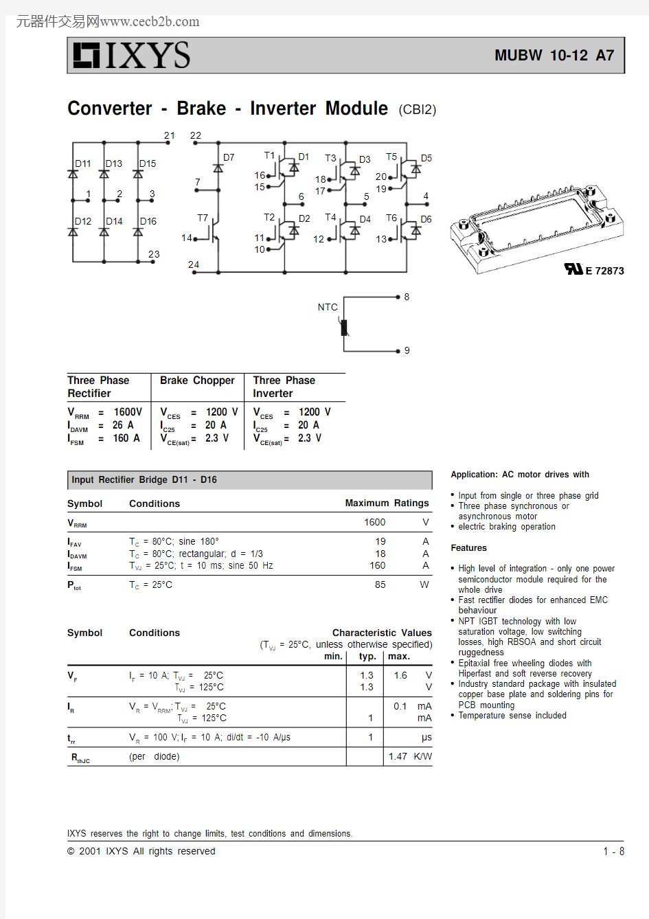
Converter - Brake - Inverter Module
(CBI2)
Symbol Conditions Maximum Ratings V
RRM
1600V
I FAV T
C
= 80°C; sine 180°19A
I DAVM T
C
= 80°C; rectangular; d = 1/318A
I FSM T
VJ
= 25°C; t = 10 ms; sine 50 Hz160A
P
tot T
C
= 25°C85W
Symbol Conditions Characteristic Values
(T
VJ = 25°C, unless otherwise specified)
min.typ.max.
V
F I
F
= 10 A; T
VJ
= 25°C 1.3 1.6V
T
VJ
= 125°C 1.3V
I R V
R
= V
RRM
;T
VJ
= 25°C0.1mA
T
VJ
= 125°C1mA
t rr V
R
= 100 V;I
F
= 10 A; di/dt = -10 A/μs1μs
R
thJC (per diode) 1.47K/W
Three Phase Brake Chopper Three Phase Rectifier Inverter
V
RRM = 1600V V
CES
= 1200 V V
CES
= 1200 V
I DAVM = 26 A I
C25
= 20 A I
C25
= 20 A
I FSM = 160 A V
CE(sat)
= 2.3 V V
CE(sat)
= 2.3 V
1
5
IXYS reserves the right to change limits, test conditions and dimensions.
8
9
Application: AC motor drives with
q Input from single or three phase grid
q Three phase synchronous or
asynchronous motor
q electric braking operation
Features
q High level of integration - only one power
semiconductor module required for the
whole drive
q Fast rectifier diodes for enhanced EMC
behaviour
q NPT IGBT technology with low
saturation voltage, low switching
losses, high RBSOA and short circuit
ruggedness
q Epitaxial free wheeling diodes with
Hiperfast and soft reverse recovery
q Industry standard package with insulated
copper base plate and soldering pins for
PCB mounting
q Temperature sense included
Symbol Conditions Maximum Ratings
V
CES T
VJ
= 25°C to 150°C1200V
V
GES
Continuous± 20V
V
GEM
Transient± 30V
I
C25T
C
= 25°C20A
I
C80T
C
= 80°C15A
RBSOA V
GE = ±15 V; R
G
= 82 ?; T
VJ
= 125°C I
CM
= 20A
Clamped inductive load; L = 100 μH V
CEK ≤ V
CES
t SC V
CE
= 720 V; V
GE
= ±15 V; R
G
= 82 ?; T
VJ
= 125°C10μs
(SCSOA)non-repetitive
P
tot T
C
= 25°C105W
Symbol Conditions Characteristic Values
(T
VJ = 25°C, unless otherwise specified)
min.typ.max.
Symbol Conditions Maximum Ratings
I
F25
T
C
= 25°C17A
I
F80
T
C
= 80°C11A
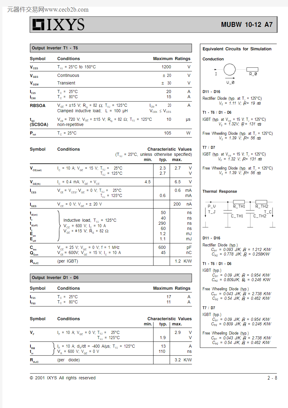
Equivalent Circuits for Simulation
Conduction
D11 - D16
Rectifier Diode (typ. at T
J
= 125°C)
V
= 1.11 V; R
= 19 m?
T1 - T6 / D1 - D6
IGBT (typ. at V
GE
= 15 V; T
J
= 125°C)
V
= 1.32V; R
= 131 m?
Free Wheeling Diode (typ. at T
J
= 125°C)
V
= 1.39 V; R
= 56 m?
T7 / D7
IGBT (typ. at V
GE
= 15 V; T
J
= 125°C)
V
= 1.32 V; R
= 131 m?
Free Wheeling Diode (typ. at T
J
= 125°C)
V
= 1.39 V; R
= 56 m?
Thermal Response
D11 - D16
Rectifier Diode (typ.)
C
th1
= 0.093 J/K; R
th1
= 1.212 K/W
C
th2
= 0.778 J/K; R
th2
= 0.258K/W
T1 - T6 / D1 - D6
IGBT (typ.)
C
th1
= 0.09 J/K; R
th1
= 0.954 K/W
C
th2
= 0.809J/K; R
th2
= 0.246 K/W
Free Wheeling Diode (typ.)
C
th1
= 0.043 J/K; R
th1
= 2.738 K/W
C
th2
= 0.54 J/K; R
th2
= 0.462 K/W
T7 / D7
IGBT (typ.)
C
th1
= 0.09 J/K; R
th1
= 0.954 K/W
C
th2
= 0.809 J/K; R
th2
= 0.246 K/W
Free Wheeling Diode (typ.)
C
th1
= 0.043 J/K; R
th1
= 2.738 K/W
C
th2
= 0.54 J/K; R
th2
= 0.462 K/W
Symbol Conditions Maximum Ratings
V CES T VJ = 25°C to 150°C 1200V V GES Continuous ± 20V V GEM Transient ± 30V I C25T C = 25°C 20A I C80T C = 80°C
15
A RBSOA V GE = ±15 V; R G = 82 ?; T VJ = 125°C I CM = 20A Clamped inductive load; L = 100 μH
V CEK ≤ V CES
t SC
V CE = 720 V; V GE = ±15 V; R G = 82 ?; T VJ = 125°C 10μs (SCSOA)non-repetitive P tot T C = 25°C 105
W
Symbol
Conditions
Characteristic Values
Symbol Conditions Maximum Ratings
V RRM T VJ = 25°C to 150°C 1200V I F25T C = 25°C 17A I F80
T C = 80°C 11
A
Symbol Conditions Characteristic Values
Dimensions in mm (1 mm = 0.0394")
01020
30
40500
100
200
300
4005000.00.4
0.8
1.21.6I F
A P tot W K/W Z thJC
Fig. 41Fig. 6Fig. 1
1
23456701234567
5
10
15
202530V CE
V V CE
A V G
-di/dt
4
6
8
10
12
1416V V GE
I 012
34
V V F
I F
Fig. 7Typ. output characteristics Fig. 8Typ. output characteristics
Fig. 9Typ. transfer characteristics
Fig. 10Typ. forward characteristics of
free wheeling diode
Fig. 11Typ. turn on gate charge
Fig. 12Typ. turn off characteristics of
free wheeling diode
Fig. 17Reverse biased safe operating area
Fig. 18Typ. transient thermal impedance
RBSOA
0.000010.00010.001
0.010.1
110
200400600
800100012001400V CE
t
s V
Fig. 19Typ. output characteristics
Fig. 20Typ. forward characteristics of
free wheeling diode
Fig. 23Typ. transient thermal impedance
Fig. 24Typ. thermistorresistance versus
temperature
1
2
3
456V V CE
I 012
3
4
5101520
2530V
V F
I F
A 0.0
0.51.01.52.0
2.5E off mJ t
0.000010.00010.001
0.01
0.1
1
10
0.0001
0.001
0.010.1110t
s Z thJC
25
50
75
100
125150
T
°C