SN74LS257B, SN74LS258B Quad 2-Input Multiplexer with 3-State Outputs
The LSTTL/MSI SN74LS257B and the SN74LS258B are Quad 2-Input Multiplexers with 3-state outputs. Four bits of data from two sources can be selected using a Common Data Select input. The four outputs present the selected data in true (non-inverted) form. The outputs may be switched to a high impedance state with a HIGH on the common Output Enable (E O) Input, allowing the outputs to interface directly with bus oriented systems. It is fabricated with the Schottky barrier diode process for high speed and is completely compatible with all ON Semiconductor TTL families.
?Schottky Process For High Speed
?Multiplexer Expansion By Tying Outputs Together
?Non-Inverting 3-State Outputs
?Input Clamp Diodes Limit High Speed Termination Effects ?Special Circuitry Ensures Glitch Free Multiplexing
?ESD > 3500 V olts
GUARANTEED OPERATING RANGES
Device Package Shipping
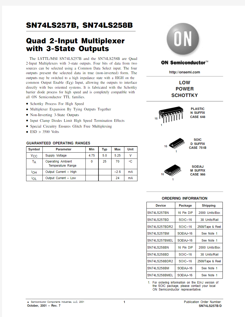
ORDERING INFORMATION
SN74LS257BN16 Pin DIP2000 Units/Box SN74LS257BD SOIC–1638 Units/Rail SN74LS257BDR2SOIC–162500/T ape & Reel SN74LS257BM SOEIAJ–16See Note 1 SN74LS257BMEL SOEIAJ–16
1.For ordering information on the EIAJ version of
the SOIC package, please contact your local
ON Semiconductor representative.
See Note 1
https://www.doczj.com/doc/088814208.html,
16 Pin DIP2000 Units/Box SN74LS258BD SOIC–1638 Units/Rail SN74LS258BDR2SOIC–162500/T ape & Reel SN74LS258BM SOEIAJ–16See Note 1 SN74LS258BMEL SOEIAJ–16See Note 1 SN74LS258BN
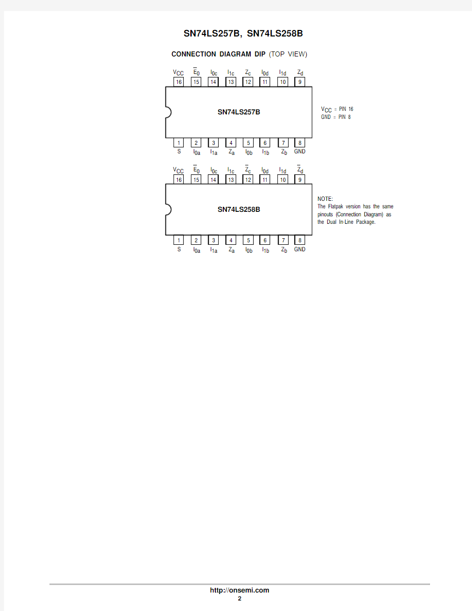
CONNECTION DIAGRAM DIP (TOP VIEW)
NOTE:
The Flatpak version has the same pinouts (Connection Diagram) as the Dual In?Line Package.
14
13
12
11
10
9
123456716
15
8V CC S E 0I 0c I 1c Z c I 1d I 0d Z d I 0a I 1a Z a I 0b I 1b Z b GND SN74LS257B
V CC = PIN 16GND = PIN 8
0a
1a a
0b
1b b
LOGIC DIAGRAMS
SN74LS257B
E
I I I I I I I I S
Z a
Z b
Z c
Z d
SN74LS258B
V CC = PIN 16GND = PIN 8
= PIN NUMBERS
E I I I I I I I I S
d
FUNCTIONAL DESCRIPTION
The LS257B and LS258B are Quad 2-Input Multiplexers with 3-state outputs. They select four bits of data from two sources each under control of a Common Data Select Input. When the Select Input is LOW, the I0 inputs are selected and when Select is HIGH, the I1 inputs are selected. The data on the selected inputs appears at the outputs in true (non-inverted) form for the LS257B and in the inverted form for the LS258B.
The LS257B and LS258B are the logic implementation of a 4-pole, 2-position switch where the position of the switch is determined by the logic levels supplied to the Select Input. The logic equations for the outputs are shown below:
When the Output Enable Input (E0) is HIGH, the outputs are forced to a high impedance “off” state. If the outputs are tied together, all but one device must be in the high impedance state to avoid high currents that would exceed the maximum ratings. Designers should ensure that Output Enable signals to 3-state devices whose outputs are tied together are designed so there is no overlap.
LS257B
Z a = E0? (I1a? S + I0a? S) Z b = E0? (I1b? S + I0b? S) Z c = E0? (I1c? S + I0c? S) Z d = E0? (I1d? S + I0d? S)LS258B
Z a = E0? (I1a? S + I0a? S) Z b = E0? (I1b? S + I0b? S) Z c = E0?(I1c? S + I0c? S) Z d = E0? (I1d? S + I0d? S)
TRUTH TABLE
H = HIGH Voltage Level
L = LOW Voltage Level
X = Don’t Care
(Z) = High Impedance (off)
(unless otherwise specified)
2.Not more than one output should be shorted at a time, nor for more than 1 second.
AC CHARACTERISTICS (T = 25°C, V = 5.0 V) See SN74LS251 for Waveforms
N SUFFIX
PLASTIC PACKAGE CASE 648–08ISSUE R
NOTES:
1.DIMENSIONING AND TOLERANCING PER ANSI Y14.5M, 198
2.
2.CONTROLLING DIMENSION: INCH.
3.DIMENSION L TO CENTER OF LEADS WHEN FORMED PARALLEL.
4.DIMENSION B DOES NOT INCLUDE MOLD FLASH.
5.
ROUNDED CORNERS OPTIONAL.
M
DIM MIN MAX MIN MAX MILLIMETERS
INCHES A 0.7400.77018.8019.55B 0.2500.270 6.35 6.85C 0.1450.175 3.69 4.44D 0.0150.0210.390.53F 0.0400.70 1.02 1.77G 0.100 BSC 2.54 BSC H 0.050 BSC 1.27 BSC J 0.0080.0150.210.38K 0.1100.130 2.80 3.30L 0.2950.3057.507.74M 0 10 0 10 S
0.0200.040
0.51 1.01
____
D SUFFIX
PLASTIC SOIC PACKAGE
CASE 751B–05
ISSUE J
NOTES:
1.DIMENSIONING AND TOLERANCING PER ANSI Y14.5M, 198
2.
2.CONTROLLING DIMENSION: MILLIMETER.
3.DIMENSIONS A AND B DO NOT INCLUDE MOLD PROTRUSION.
4.MAXIMUM MOLD PROTRUSION 0.15 (0.006)PER SIDE.
5.DIMENSION D DOES NOT INCLUDE DAMBAR PROTRUSION. ALLOWABLE DAMBAR
PROTRUSION SHALL BE 0.127 (0.005) TOTAL IN EXCESS OF THE D DIMENSION AT MAXIMUM MATERIAL CONDITION.
S
B
M
0.25 (0.010)A
S
T DIM MIN MAX MIN MAX INCHES
MILLIMETERS A 9.8010.000.3860.393B 3.80 4.000.1500.157C 1.35 1.750.0540.068D 0.350.490.0140.019F 0.40 1.250.0160.049G 1.27 BSC 0.050 BSC J 0.190.250.0080.009K 0.100.250.0040.009M 0 7 0 7 P 5.80 6.200.2290.244R
0.250.50
0.0100.019
____
NOTES:
1.DIMENSIONING AND TOLERANCING PER ANSI Y14.5M, 198
2.
M SUFFIX SOEIAJ PACKAGE CASE 966–01ISSUE O
ON Semiconductor and are trademarks of Semiconductor Components Industries, LLC (SCILLC). SCILLC reserves the right to make changes without further notice to any products herein. SCILLC makes no warranty, representation or guarantee regarding the suitability of its products for any particular purpose, nor does SCILLC assume any liability arising out of the application or use of any product or circuit, and specifically disclaims any and all liability,including without limitation special, consequential or incidental damages. “Typical” parameters which may be provided in SCILLC data sheets and/or specifications can and do vary in different applications and actual performance may vary over time. All operating parameters, including “Typicals” must be validated for each customer application by customer’s technical experts. SCILLC does not convey any license under its patent rights nor the rights of others.SCILLC products are not designed, intended, or authorized for use as components in systems intended for surgical implant into the body, or other applications intended to support or sustain life, or for any other application in which the failure of the SCILLC product could create a situation where personal injury or death may occur. Should Buyer purchase or use SCILLC products for any such unintended or unauthorized application, Buyer shall indemnify and hold SCILLC and its officers, employees, subsidiaries, affiliates, and distributors harmless against all claims, costs, damages, and expenses, and reasonable attorney fees arising out of, directly or indirectly, any claim of personal injury or death associated with such unintended or unauthorized use, even if such claim alleges that SCILLC was negligent regarding the design or manufacture of the part. SCILLC is an Equal Opportunity/Affirmative Action Employer.
PUBLICATION ORDERING INFORMATION
JAPAN : ON Semiconductor, Japan Customer Focus Center
4–32–1 Nishi–Gotanda, Shinagawa–ku, Tokyo, Japan 141–0031Phone : 81–3–5740–2700Email : r14525@https://www.doczj.com/doc/088814208.html,