
Rev.3.3_00
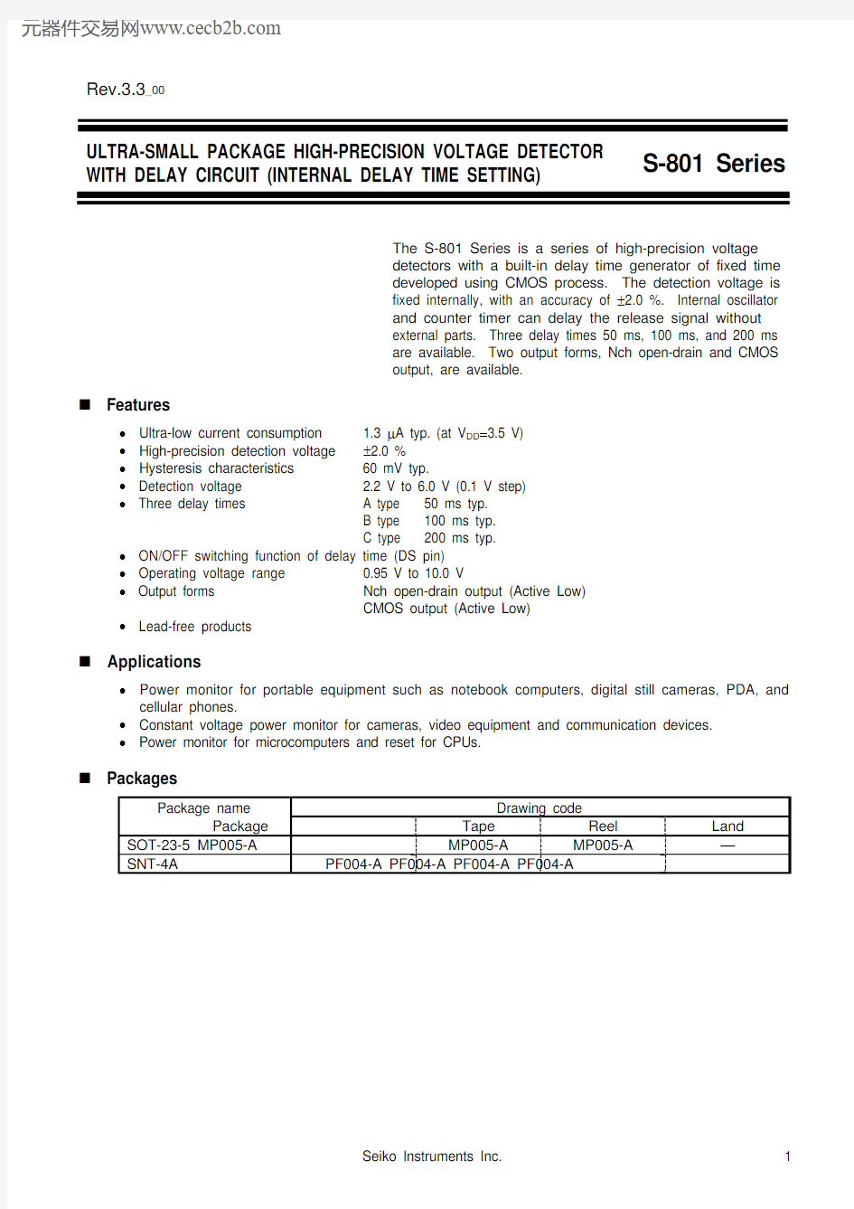
ULTRA-SMALL PACKAGE HIGH-PRECISION VOLTAGE DETECTOR
S-801 Series
WITH DELAY CIRCUIT (INTERNAL DELAY TIME SETTING)
The S-801 Series is a series of high-precision voltage
detectors with a built-in delay time generator of fixed time
developed using CMOS process. The detection voltage is
fixed internally, with an accuracy of ±2.0 %. Internal oscillator
and counter timer can delay the release signal without
external parts. Three delay times 50 ms, 100 ms, and 200 ms
are available. Two output forms, Nch open-drain and CMOS
output, are available.
Features
? Ultra-low current consumption 1.3 μA typ. (at V DD=3.5 V)
? High-precision detection voltage ±2.0 %
? Hysteresis characteristics 60 mV typ.
? Detection voltage 2.2 V to 6.0 V (0.1 V step)
? Three delay times A type 50 ms typ.
B type 100 ms typ.
C type 200 ms typ.
? ON/OFF switching function of delay time (DS pin)
? Operating voltage range 0.95 V to 10.0 V
? Output forms Nch open-drain output (Active Low)
CMOS output (Active Low)
? Lead-free products
Applications
? Power monitor for portable equipment such as notebook computers, digital still cameras, PDA, and cellular phones.
? Constant voltage power monitor for cameras, video equipment and communication devices.
? Power monitor for microcomputers and reset for CPUs.
Packages
Package name Drawing code
Reel
Land
Tape
Package
MP005-A
—
MP005-A
SOT-23-5 MP005-A
SNT-4A PF004-A PF004-A PF004-A PF004-A
S-801 Series
Rev.3.3_00
Block Diagrams
1. Nch Open-drain Output Products
DS
OUT
VSS
VDD
*1. Parasitic diode
Figure 1
2. CMOS Output Products
OUT
DS
VSS
VDD
*1. Parasitic diode
Figure 2
Rev.3.3_00S-801 Series
Product Name Structure
The detection voltage, delay time, output form and packages for S-801 Series can be selected at the user's request. Refer to the "1. Product name" for the construction of the product name and "2. Product Name List" for the full product names.
1. Product Name
S-801xx x x xx - xxx xx G
*1
*2. Refer to the Table 2 in the “2. Product name list”.
S-801 Series Rev.3.3_00
2. Product Name List
2-1. SOT-23-5
Table 1 (1/3)
Detection voltage range Delay time Nch open-drain output products CMOS output products
2.2 V ±2.0% 50 ms typ. S-80122ANMC-JCHT2G S-80122ALMC-JAHT2G
100 ms typ. S-80122BNMC-JGHT2G S-80122BLMC-JEHT2G
200 ms typ. S-80122CNMC-JKHT2G S-80122CLMC-JIHT2G
2.3 V ±2.0% 50 ms typ. S-80123ANMC-JCIT2G S-80123ALMC-JAIT2G
100 ms typ. S-80123BNMC-JGIT2G S-80123BLMC-JEIT2G
200 ms typ. S-80123CNMC-JKIT2G S-80123CLMC-JIIT2G
2.4 V ±2.0% 50 ms typ. S-80124ANMC-JCJT2G S-80124ALMC-JAJT2G
100 ms typ. S-80124BNMC-JGJT2G S-80124BLMC-JEJT2G
200 ms typ. S-80124CNMC-JKJT2G S-80124CLMC-JIJT2G
2.5 V ±2.0% 50 ms typ. S-80125ANMC-JCKT2G S-80125ALMC-JAKT2G
100 ms typ. S-80125BNMC-JGKT2G S-80125BLMC-JEKT2G
200 ms typ. S-80125CNMC-JKKT2G S-80125CLMC-JIKT2G
2.6 V ±2.0% 50 ms typ. S-80126ANMC-JCLT2G S-80126ALMC-JALT2G
100 ms typ. S-80126BNMC-JGLT2G S-80126BLMC-JELT2G
200 ms typ. S-80126CNMC-JKLT2G S-80126CLMC-JILT2G
2.7 V ±2.0% 50 ms typ. S-80127ANMC-JCMT2G S-80127ALMC-JAMT2G
100 ms typ. S-80127BNMC-JGMT2G S-80127BLMC-JEMT2G
200 ms typ. S-80127CNMC-JKMT2G S-80127CLMC-JIMT2G
2.8 V ±2.0% 50 ms typ. S-80128ANMC-JCNT2G S-80128ALMC-JANT2G
100 ms typ. S-80128BNMC-JGNT2G S-80128BLMC-JENT2G
200 ms typ. S-80128CNMC-JKNT2G S-80128CLMC-JINT2G
2.9 V ±2.0% 50 ms typ. S-80129ANMC-JCOT2G S-80129ALMC-JAOT2G
100 ms typ. S-80129BNMC-JGOT2G S-80129BLMC-JEOT2G
200 ms typ. S-80129CNMC-JKOT2G S-80129CLMC-JIOT2G
3.0 V ±2.0% 50 ms typ. S-80130ANMC-JCPT2G S-80130ALMC-JAPT2G
100 ms typ. S-80130BNMC-JGPT2G S-80130BLMC-JEPT2G
200 ms typ. S-80130CNMC-JKPT2G S-80130CLMC-JIPT2G
3.1 V ±2.0% 50 ms typ. S-80131ANMC-JCQT2G S-80131ALMC-JAQT2G
100 ms typ. S-80131BNMC-JGQT2G S-80131BLMC-JEQT2G
200 ms typ. S-80131CNMC-JKQT2G S-80131CLMC-JIQT2G
3.2 V ±2.0% 50 ms typ. S-80132ANMC-JCRT2G S-80132ALMC-JART2G
100 ms typ. S-80132BNMC-JGRT2G S-80132BLMC-JERT2G
200 ms typ. S-80132CNMC-JKRT2G S-80132CLMC-JIRT2G
3.3 V ±2.0% 50 ms typ. S-80133ANMC-JCST2G S-80133ALMC-JAST2G
100 ms typ. S-80133BNMC-JGST2G S-80133BLMC-JEST2G
200 ms typ. S-80133CNMC-JKST2G S-80133CLMC-JIST2G
3.4 V ±2.0% 50 ms typ. S-80134ANMC-JCTT2G S-80134ALMC-JATT2G
100 ms typ. S-80134BNMC-JGTT2G S-80134BLMC-JETT2G
200 ms typ. S-80134CNMC-JKTT2G S-80134CLMC-JITT2G
Rev.3.3_00S-801 Series
Table 1 (2/3)
Detection voltage range Delay time Nch open-drain output products CMOS output products
3.5 V ±2.0% 50 ms typ. S-80135ANMC-JCUT2G S-80135ALMC-JAUT2G
100 ms typ. S-80135BNMC-JGUT2G S-80135BLMC-JEUT2G
200 ms typ. S-80135CNMC-JKUT2G S-80135CLMC-JIUT2G
3.6 V ±2.0% 50 ms typ. S-80136ANMC-JCVT2G S-80136ALMC-JAVT2G
100 ms typ. S-80136BNMC-JGVT2G S-80136BLMC-JEVT2G
200 ms typ. S-80136CNMC-JKVT2G S-80136CLMC-JIVT2G
3.7 V ±2.0% 50 ms typ. S-80137ANMC-JCWT2G S-80137ALMC-JAWT2G
100 ms typ. S-80137BNMC-JGWT2G S-80137BLMC-JEWT2G
200 ms typ. S-80137CNMC-JKWT2G S-80137CLMC-JIWT2G
3.8 V ±2.0% 50 ms typ. S-80138ANMC-JCXT2G S-80138ALMC-JAXT2G
100 ms typ. S-80138BNMC-JGXT2G S-80138BLMC-JEXT2G
200 ms typ. S-80138CNMC-JKXT2G S-80138CLMC-JIXT2G
3.9 V ±2.0% 50 ms typ. S-80139ANMC-JCYT2G S-80139ALMC-JAYT2G
100 ms typ. S-80139BNMC-JGYT2G S-80139BLMC-JEYT2G
200 ms typ. S-80139CNMC-JKYT2G S-80139CLMC-JIYT2G
4.0 V ±2.0% 50 ms typ. S-80140ANMC-JCZT2G S-80140ALMC-JAZT2G
100 ms typ. S-80140BNMC-JGZT2G S-80140BLMC-JEZT2G
200 ms typ. S-80140CNMC-JKZT2G S-80140CLMC-JIZT2G
4.1 V ±2.0% 50 ms typ. S-80141ANMC-JC2T2G S-80141ALMC-JA2T2G
100 ms typ. S-80141BNMC-JG2T2G S-80141BLMC-JE2T2G
200 ms typ. S-80141CNMC-JK2T2G S-80141CLMC-JI2T2G
4.2 V ±2.0% 50 ms typ. S-80142ANMC-JC3T2G S-80142ALMC-JA3T2G
100 ms typ. S-80142BNMC-JG3T2G S-80142BLMC-JE3T2G
200 ms typ. S-80142CNMC-JK3T2G S-80142CLMC-JI3T2G
4.3 V ±2.0% 50 ms typ. S-80143ANMC-JC4T2G S-80143ALMC-JA4T2G
100 ms typ. S-80143BNMC-JG4T2G S-80143BLMC-JE4T2G
200 ms typ. S-80143CNMC-JK4T2G S-80143CLMC-JI4T2G
4.4 V ±2.0% 50 ms typ. S-80144ANMC-JC5T2G S-80144ALMC-JA5T2G
100 ms typ. S-80144BNMC-JG5T2G S-80144BLMC-JE5T2G
200 ms typ. S-80144CNMC-JK5T2G S-80144CLMC-JI5T2G
4.5 V ±2.0% 50 ms typ. S-80145ANMC-JC6T2G S-80145ALMC-JA6T2G
100 ms typ. S-80145BNMC-JG6T2G S-80145BLMC-JE6T2G
200 ms typ. S-80145CNMC-JK6T2G S-80145CLMC-JI6T2G
4.6 V ±2.0% 50 ms typ. S-80146ANMC-JC7T2G S-80146ALMC-JA7T2G
100 ms typ. S-80146BNMC-JG7T2G S-80146BLMC-JE7T2G
200 ms typ. S-80146CNMC-JK7T2G S-80146CLMC-JI7T2G
4.7 V ±2.0% 50 ms typ. S-80147ANMC-JC8T2G S-80147ALMC-JA8T2G
100 ms typ. S-80147BNMC-JG8T2G S-80147BLMC-JE8T2G
200 ms typ. S-80147CNMC-JK8T2G S-80147CLMC-JI8T2G
4.8 V ±2.0% 50 ms typ. S-80148ANMC-JC9T2G S-80148ALMC-JA9T2G
100 ms typ. S-80148BNMC-JG9T2G S-80148BLMC-JE9T2G
200 ms typ. S-80148CNMC-JK9T2G S-80148CLMC-JI9T2G
4.9 V ±2.0% 50 ms typ. S-80149ANMC-JDAT2G S-80149ALMC-JBAT2G
100 ms typ. S-80149BNMC-JHAT2G S-80149BLMC-JFAT2G
200 ms typ. S-80149CNMC-JLAT2G S-80149CLMC-JJAT2G
S-801 Series Rev.3.3_00
Table 1 (3/3)
Detection voltage range Delay time Nch open-drain output products CMOS output products
5.0 V ±2.0% 50 ms typ. S-80150ANMC-JDBT2G S-80150ALMC-JBBT2G
100 ms typ. S-80150BNMC-JHBT2G S-80150BLMC-JFBT2G
200 ms typ. S-80150CNMC-JLBT2G S-80150CLMC-JJBT2G
5.1 V ±2.0% 50 ms typ. S-80151ANMC-JDCT2G S-80151ALMC-JBCT2G
100 ms typ. S-80151BNMC-JHCT2G S-80151BLMC-JFCT2G
200 ms typ. S-80151CNMC-JLCT2G S-80151CLMC-JJCT2G
5.2 V ±2.0% 50 ms typ. S-80152ANMC-JDDT2G S-80152ALMC-JBDT2G
100 ms typ. S-80152BNMC-JHDT2G S-80152BLMC-JFDT2G
200 ms typ. S-80152CNMC-JLDT2G S-80152CLMC-JJDT2G
5.3 V ±2.0% 50 ms typ. S-80153ANMC-JDET2G S-80153ALMC-JBET2G
100 ms typ. S-80153BNMC-JHET2G S-80153BLMC-JFET2G
200 ms typ. S-80153CNMC-JLET2G S-80153CLMC-JJET2G
5.4 V ±2.0% 50 ms typ. S-80154ANMC-JDFT2G S-80154ALMC-JBFT2G
100 ms typ. S-80154BNMC-JHFT2G S-80154BLMC-JFFT2G
200 ms typ. S-80154CNMC-JLFT2G S-80154CLMC-JJFT2G
5.5 V ±2.0% 50 ms typ. S-80155ANMC-JDGT2G S-80155ALMC-JBGT2G
100 ms typ. S-80155BNMC-JHGT2G S-80155BLMC-JFGT2G
200 ms typ. S-80155CNMC-JLGT2G S-80155CLMC-JJGT2G
5.6 V ±2.0% 50 ms typ. S-80156ANMC-JDHT2G S-80156ALMC-JBHT2G
100 ms typ. S-80156BNMC-JHHT2G S-80156BLMC-JFHT2G
200 ms typ. S-80156CNMC-JLHT2G S-80156CLMC-JJHT2G
5.7 V ±2.0% 50 ms typ. S-80157ANMC-JDIT2G S-80157ALMC-JBIT2G
100 ms typ. S-80157BNMC-JHIT2G S-80157BLMC-JFIT2G
200 ms typ. S-80157CNMC-JLIT2G S-80157CLMC-JJIT2G
5.8 V ±2.0% 50 ms typ. S-80158ANMC-JDJT2G S-80158ALMC-JBJT2G
100 ms typ. S-80158BNMC-JHJT2G S-80158BLMC-JFJT2G
200 ms typ. S-80158CNMC-JLJT2G S-80158CLMC-JJJT2G
5.9 V ±2.0% 50 ms typ. S-80159ANMC-JDKT2G S-80159ALMC-JBKT2G
100 ms typ. S-80159BNMC-JHKT2G S-80159BLMC-JFKT2G
200 ms typ. S-80159CNMC-JLKT2G S-80159CLMC-JJKT2G
6.0 V ±2.0% 50 ms typ. S-80160ANMC-JDLT2G S-80160ALMC-JBLT2G
100 ms typ. S-80160BNMC-JHLT2G S-80160BLMC-JFLT2G
200 ms typ. S-80160CNMC-JLLT2G S-80160CLMC-JJLT2G
Rev.3.3_00S-801 Series
2-2. SNT-4A
Table 2 (1/3)
Detection voltage range Delay time Nch open-drain output products CMOS output products
2.2 V ±2.0% 50 ms typ. S-80122ANPF-JCHTFG S-80122ALPF-JAHTFG
100 ms typ. S-80122BNPF-JGHTFG S-80122BLPF-JEHTFG
200 ms typ. S-80122CNPF-JKHTFG S-80122CLPF-JIHTFG
2.3 V ±2.0% 50 ms typ. S-80123ANPF-JCITFG S-80123ALPF-JAITFG
100 ms typ. S-80123BNPF-JGITFG S-80123BLPF-JEITFG
200 ms typ. S-80123CNPF-JKITFG S-80123CLPF-JIITFG
2.4 V ±2.0% 50 ms typ. S-80124ANPF-JCJTFG S-80124ALPF-JAJTFG
100 ms typ. S-80124BNPF-JGJTFG S-80124BLPF-JEJTFG
200 ms typ. S-80124CNPF-JKJTFG S-80124CLPF-JIJTFG
2.5 V ±2.0% 50 ms typ. S-80125ANPF-JCKTFG S-80125ALPF-JAKTFG
100 ms typ. S-80125BNPF-JGKTFG S-80125BLPF-JEKTFG
200 ms typ. S-80125CNPF-JKKTFG S-80125CLPF-JIKTFG
2.6 V ±2.0% 50 ms typ. S-80126ANPF-JCLTFG S-80126ALPF-JALTFG
100 ms typ. S-80126BNPF-JGLTFG S-80126BLPF-JELTFG
200 ms typ. S-80126CNPF-JKLTFG S-80126CLPF-JILTFG
2.7 V ±2.0% 50 ms typ. S-80127ANPF-JCMTFG S-80127ALPF-JAMTFG
100 ms typ. S-80127BNPF-JGMTFG S-80127BLPF-JEMTFG
200 ms typ. S-80127CNPF-JKMTFG S-80127CLPF-JIMTFG
2.8 V ±2.0% 50 ms typ. S-80128ANPF-JCNTFG S-80128ALPF-JANTFG
100 ms typ. S-80128BNPF-JGNTFG S-80128BLPF-JENTFG
200 ms typ. S-80128CNPF-JKNTFG S-80128CLPF-JINTFG
2.9 V ±2.0% 50 ms typ. S-80129ANPF-JCOTFG S-80129ALPF-JAOTFG
100 ms typ. S-80129BNPF-JGOTFG S-80129BLPF-JEOTFG
200 ms typ. S-80129CNPF-JKOTFG S-80129CLPF-JIOTFG
3.0 V ±2.0% 50 ms typ. S-80130ANPF-JCPTFG S-80130ALPF-JAPTFG
100 ms typ. S-80130BNPF-JGPTFG S-80130BLPF-JEPTFG
200 ms typ. S-80130CNPF-JKPTFG S-80130CLPF-JIPTFG
3.1 V ±2.0% 50 ms typ. S-80131ANPF-JCQTFG S-80131ALPF-JAQTFG
100 ms typ. S-80131BNPF-JGQTFG S-80131BLPF-JEQTFG
200 ms typ. S-80131CNPF-JKQTFG S-80131CLPF-JIQTFG
3.2 V ±2.0% 50 ms typ. S-80132ANPF-JCRTFG S-80132ALPF-JARTFG
100 ms typ. S-80132BNPF-JGRTFG S-80132BLPF-JERTFG
200 ms typ. S-80132CNPF-JKRTFG S-80132CLPF-JIRTFG
3.3 V ±2.0% 50 ms typ. S-80133ANPF-JCSTFG S-80133ALPF-JASTFG
100 ms typ. S-80133BNPF-JGSTFG S-80133BLPF-JESTFG
200 ms typ. S-80133CNPF-JKSTFG S-80133CLPF-JISTFG
3.4 V ±2.0% 50 ms typ. S-80134ANPF-JCTTFG S-80134ALPF-JATTFG
100 ms typ. S-80134BNPF-JGTTFG S-80134BLPF-JETTFG
200 ms typ. S-80134CNPF-JKTTFG S-80134CLPF-JITTFG
3.5 V ±2.0% 50 ms typ. S-80135ANPF-JCUTFG S-80135ALPF-JAUTFG
100 ms typ. S-80135BNPF-JGUTFG S-80135BLPF-JEUTFG
200 ms typ. S-80135CNPF-JKUTFG S-80135CLPF-JIUTFG
3.6 V ±2.0% 50 ms typ. S-80136ANPF-JCVTFG S-80136ALPF-JAVTFG
100 ms typ. S-80136BNPF-JGVTFG S-80136BLPF-JEVTFG
200 ms typ. S-80136CNPF-JKVTFG S-80136CLPF-JIVTFG
3.7 V ±2.0% 50 ms typ. S-80137ANPF-JCWTFG S-80137ALPF-JAWTFG
100 ms typ. S-80137BNPF-JGWTFG S-80137BLPF-JEWTFG
200 ms typ. S-80137CNPF-JKWTFG S-80137CLPF-JIWTFG
S-801 Series Rev.3.3_00
Table 2 (2/3)
Detection voltage range Delay time Nch open-drain output products CMOS output products
3.8 V ±2.0% 50 ms typ. S-80138ANPF-JCXTFG S-80138ALPF-JAXTFG
100 ms typ. S-80138BNPF-JGXTFG S-80138BLPF-JEXTFG
200 ms typ. S-80138CNPF-JKXTFG S-80138CLPF-JIXTFG
3.9 V ±2.0% 50 ms typ. S-80139ANPF-JCYTFG S-80139ALPF-JAYTFG
100 ms typ. S-80139BNPF-JGYTFG S-80139BLPF-JEYTFG
200 ms typ. S-80139CNPF-JKYTFG S-80139CLPF-JIYTFG
4.0 V ±2.0% 50 ms typ. S-80140ANPF-JCZTFG S-80140ALPF-JAZTFG
100 ms typ. S-80140BNPF-JGZTFG S-80140BLPF-JEZTFG
200 ms typ. S-80140CNPF-JKZTFG S-80140CLPF-JIZTFG
4.1 V ±2.0% 50 ms typ. S-80141ANPF-JC2TFG S-80141ALPF-JA2TFG
100 ms typ. S-80141BNPF-JG2TFG S-80141BLPF-JE2TFG
200 ms typ. S-80141CNPF-JK2TFG S-80141CLPF-JI2TFG
4.2 V ±2.0% 50 ms typ. S-80142ANPF-JC3TFG S-80142ALPF-JA3TFG
100 ms typ. S-80142BNPF-JG3TFG S-80142BLPF-JE3TFG
200 ms typ. S-80142CNPF-JK3TFG S-80142CLPF-JI3TFG
4.3 V ±2.0% 50 ms typ. S-80143ANPF-JC4TFG S-80143ALPF-JA4TFG
100 ms typ. S-80143BNPF-JG4TFG S-80143BLPF-JE4TFG
200 ms typ. S-80143CNPF-JK4TFG S-80143CLPF-JI4TFG
4.4 V ±2.0% 50 ms typ. S-80144ANPF-JC5TFG S-80144ALPF-JA5TFG
100 ms typ. S-80144BNPF-JG5TFG S-80144BLPF-JE5TFG
200 ms typ. S-80144CNPF-JK5TFG S-80144CLPF-JI5TFG
4.5 V ±2.0% 50 ms typ. S-80145ANPF-JC6TFG S-80145ALPF-JA6TFG
100 ms typ. S-80145BNPF-JG6TFG S-80145BLPF-JE6TFG
200 ms typ. S-80145CNPF-JK6TFG S-80145CLPF-JI6TFG
4.6 V ±2.0% 50 ms typ. S-80146ANPF-JC7TFG S-80146ALPF-JA7TFG
100 ms typ. S-80146BNPF-JG7TFG S-80146BLPF-JE7TFG
200 ms typ. S-80146CNPF-JK7TFG S-80146CLPF-JI7TFG
4.7 V ±2.0% 50 ms typ. S-80147ANPF-JC8TFG S-80147ALPF-JA8TFG
100 ms typ. S-80147BNPF-JG8TFG S-80147BLPF-JE8TFG
200 ms typ. S-80147CNPF-JK8TFG S-80147CLPF-JI8TFG
4.8 V ±2.0% 50 ms typ. S-80148ANPF-JC9TFG S-80148ALPF-JA9TFG
100 ms typ. S-80148BNPF-JG9TFG S-80148BLPF-JE9TFG
200 ms typ. S-80148CNPF-JK9TFG S-80148CLPF-JI9TFG
4.9 V ±2.0% 50 ms typ. S-80149ANPF-JDATFG S-80149ALPF-JBATFG
100 ms typ. S-80149BNPF-JHATFG S-80149BLPF-JFATFG
200 ms typ. S-80149CNPF-JLATFG S-80149CLPF-JJATFG
5.0 V ±2.0% 50 ms typ. S-80150ANPF-JDBTFG S-80150ALPF-JBBTFG
100 ms typ. S-80150BNPF-JHBTFG S-80150BLPF-JFBTFG
200 ms typ. S-80150CNPF-JLBTFG S-80150CLPF-JJBTFG
5.1 V ±2.0% 50 ms typ. S-80151ANPF-JDCTFG S-80151ALPF-JBCTFG
100 ms typ. S-80151BNPF-JHCTFG S-80151BLPF-JFCTFG
200 ms typ. S-80151CNPF-JLCTFG S-80151CLPF-JJCTFG
5.2 V ±2.0% 50 ms typ. S-80152ANPF-JDDTFG S-80152ALPF-JBDTFG
100 ms typ. S-80152BNPF-JHDTFG S-80152BLPF-JFDTFG
200 ms typ. S-80152CNPF-JLDTFG S-80152CLPF-JJDTFG
5.3 V ±2.0% 50 ms typ. S-80153ANPF-JDETFG S-80153ALPF-JBETFG
100 ms typ. S-80153BNPF-JHETFG S-80153BLPF-JFETFG
200 ms typ. S-80153CNPF-JLETFG S-80153CLPF-JJETFG
Rev.3.3_00S-801 Series
Table 2 (3/3)
Detection voltage range Delay time Nch open-drain output products CMOS output products
5.4 V ±2.0% 50 ms typ. S-80154ANPF-JDFTFG S-80154ALPF-JBFTFG
100 ms typ. S-80154BNPF-JHFTFG S-80154BLPF-JFFTFG
200 ms typ. S-80154CNPF-JLFTFG S-80154CLPF-JJFTFG
5.5 V ±2.0% 50 ms typ. S-80155ANPF-JDGTFG S-80155ALPF-JBGTFG
100 ms typ. S-80155BNPF-JHGTFG S-80155BLPF-JFGTFG
200 ms typ. S-80155CNPF-JLGTFG S-80155CLPF-JJGTFG
5.6 V ±2.0% 50 ms typ. S-80156ANPF-JDHTFG S-80156ALPF-JBHTFG
100 ms typ. S-80156BNPF-JHHTFG S-80156BLPF-JFHTFG
200 ms typ. S-80156CNPF-JLHTFG S-80156CLPF-JJHTFG
5.7 V ±2.0% 50 ms typ. S-80157ANPF-JDITFG S-80157ALPF-JBITFG
100 ms typ. S-80157BNPF-JHITFG S-80157BLPF-JFITFG
200 ms typ. S-80157CNPF-JLITFG S-80157CLPF-JJITFG
5.8 V ±2.0% 50 ms typ. S-80158ANPF-JDJTFG S-80158ALPF-JBJTFG
100 ms typ. S-80158BNPF-JHJTFG S-80158BLPF-JFJTFG
200 ms typ. S-80158CNPF-JLJTFG S-80158CLPF-JJJTFG
5.9 V ±2.0% 50 ms typ. S-80159ANPF-JDKTFG S-80159ALPF-JBKTFG
100 ms typ. S-80159BNPF-JHKTFG S-80159BLPF-JFKTFG
200 ms typ. S-80159CNPF-JLKTFG S-80159CLPF-JJKTFG
6.0 V ±2.0% 50 ms typ. S-80160ANPF-JDLTFG S-80160ALPF-JBLTFG
100 ms typ. S-80160BNPF-JHLTFG S-80160BLPF-JFLTFG
200 ms typ. S-80160CNPF-JLLTFG S-80160CLPF-JJLTFG
S-801 Series Rev.3.3_00
Pin Configurations
Table 3
Pin No. Pin name Pin description
1
DS*1ON/OFF switch for delay time
2
VSS
GND
pin
3
NC*2 No
connection
4 OUT Voltage detection output pin
5 VDD Voltage input pin
SOT-23-5
Top view
Figure 3
*1. Refer to “2. Delay Circuit” in “ Operation” for operation.
*2. The NC pin is electrically open.
The NC pin can be connected to VDD or VSS.
Table 4
Pin No. Pin name Pin description
1
VSS
GND
pin
2
DS*1ON/OFF switch for delay time
3 VDD Voltage input pin
4 OUT Voltage detection output pin
SNT-4A
Top view
4
2 3
Figure 4
*1. Refer to “2. Delay Circuit” in “ Operation” for operation.
Rev.3.3_00 S-801 Series
Absolute Maximum Ratings
Table 5
(Ta =25°C unless otherwise specified)
Item Symbol Absolute maximum ratings Unit
Power supply voltage V DD ?V SS
12 V Output voltage Nch open-drain output products V OUT V SS ?0.3 to V SS +12
CMOS output products V SS ?0.3 to V
DD +0.3
Output current I OUT 50 mA SOT-23-5 P D 250 (When not mounted on board) mW 600*1
SNT-4A 140 (When not mounted on board)
Power dissipation 300*1
Operating ambient temperature T opr ?40 to +85 °C Storage temperature T stg ?40 to +125 *1. When mounted on board [Mounted board]
(1) Board size: 114.3 mm × 76.2 mm × t1.6 mm (2) Board name: JEDEC STANDARD51-7
Caution The absolute maximum ratings are rated values exceeding which the product could suffer
physical damage. These values must therefore not be exceeded under any conditions.
P o w e r D i s s i p a t i o n (P D ) [m W ]
Figure 5 Power Dissipation of Package (When Mounted on Board)
S-801 Series
Rev.3.3_00
Electrical Characteristics
Table 6
DET DET(S)detection voltage range in Table 1 to 2.)
*2. Temperature change ratio for the detection voltage [mV/°C] is calculated using the following equation.
[]()[][]1000C ppm/ V Ta ΔV ΔV Typ.V C mV/ Ta ΔV ΔDET
DET DET(S)DET ÷°??×?=°??3
*2**1 *1. Temperature change ratio of the detection voltage *2. Specified detection voltage value
*3. Detection voltage temperature coefficient
Rev.3.3_00S-801 Series Test Circuits
1.
R*1
100 kΩ
2.
*1. R is unnecessary for CMOS output products.
Figure 6 Figure 7
3.
R*1
100 kΩ4.
R*1
100 kΩ
*1. R is unnecessary for CMOS output products.*1. R is unnecessary for CMOS output products.
Figure 8 Figure 9
S-801 Series
Rev.3.3_00
Operation
1. Basic Operation: CMOS Output (Active Low)
1-1. When the power supply voltage (V DD ) is higher than the release voltage (+V DET ), the Nch
transistor is OFF and the Pch transistor is ON to provide V DD (high) at the output. Since the
Nch transistor N1 in Figure 10 is OFF, the comparator input voltage is C B A DD
C B R R R V )R R (++?+.
1-2. When the V DD goes below +V DET , the output provides the V DD level, as long as V DD remains
above the detection voltage (–V DET ). When the V DD falls below –V DET (point A in Figure 11), the Nch transistor becomes ON, the Pch transistor becomes OFF, and the V SS level appears at the output. At this time the Nch transistor N1 in Figure 10 becomes ON, the comparator
input voltage is changed to
B A DD
B R R V R +?. 1-3. When the V DD falls below the minimum operating voltage, the output becomes undefined, or
goes to V DD when the output is pulled up to V DD . 1-4. The V SS level appears when V DD rises above the minimum operating voltage. The V SS level still
appears even when V DD surpasses the –V DET , as long as it does not exceed the release voltage +V DET . 1-5. When V DD rises above +V DET (point B in Figure 11), the Nch transistor becomes OFF and the
Pch transistor becomes ON to provide V DD at the output. The V DD at the OUT pin is delayed for t D due to the delay circuit.
OUT
*1. Paracitic diode
Figure 10 Operation 1
Rev.3.3_00 S-801 Series
+V DET )
?V DET )
Figure 11 Operation 2
2. Delay Circuit
2-1. Delay Time
The delay circuit delays the output signal from the time at which the power voltage (V DD ) exceeds the release voltage (+V DET ) when V DD is turned on. The output signal is not delayed when the V DD goes below the detection voltage (–V DET ). (Refer to Figure 11.)
The delay time (t D ) is a fixed value that is determined by a built-in oscillation circuit and counter.
2-2. DS Pin (ON/OFF Switch Pin for Delay Time)
The DS pin should be connected to Low or High. When the DS pin is High, the output delay time becomes short since the output signal is taken from the middle of counter circuit (Refer to Figure 16).
3. Other Characteristics
3-1. Temperature Characteristics of Detection Voltage
The shaded area in Figure 12 shows the temperature characteristics of the detection voltage.
°C
°C] °C
–V DET
Figure 12 Temperature Characteristics of Detection Voltage (Example for S-80122xxxx)
S-801 Series
Rev.3.3_00
3-2. Temperature Characteristics of Release Voltage
The temperature coefficient Ta
V DET
Δ+Δ of the release voltage is calculated by the temperature
coefficient Ta
V DET
Δ?Δfor the detection voltage as follows:
Ta
V V V Ta
V DET DET DET DET Δ?Δ×?+=Δ+Δ
The temperature coefficients for the release voltage and the detection voltage have the same sign consequently.
3-3. Temperature Characteristics of Hysteresis Voltage
The temperature characteristics for the hysteresis voltage is expressed as Ta
V Ta V DET
DET Δ?Δ?
Δ+Δ and is calculated as follows: Ta V V V Ta V Ta V DET
DET HYS DET DET Δ?Δ×
?=Δ?Δ?Δ+Δ
Standard Circuit
*1. R is unnecessary for CMOS output products.
Figure 13
Caution The above connection diagram and constant will not guarantees successful operation.
Perform through using the actual application to set the constant.
Rev.3.3_00 S-801 Series
Technical Terms
1. Detection Voltage (–V DET ), Release Voltage (+V DET )
The detection voltage (–V DET ) is a voltage at which the output turns to low. The detection voltage varies slightly among products of the same specification. The variation of detection voltage between the specified minimum (–V DET ) Min. and the maximum (–V DET ) Max. is called the detection voltage range (Refer to Figure 14).
e.g. For the S-80122AN, the detection voltage lies in the range of 2.156 ≤ (–V DET ) ≤ 2.244.
This means that some S-80122ANs have 2.156 V for –V DET and some have 2.244 V.
The release voltage (+V DET ) is a voltage at which the output turns to high. The release voltage varies slightly among products of the same specification. The variation of release voltages between the specified minimum (+V DET ) Min. and the maximum (+V DET ) Max. is called the release voltage range (Refer to Figure 15).
e.g. For the S-80122AN, the release voltage lies in the range of 2.186 ≤ (+V DET ) ≤ 2.344.
This means that some S-80122ANs have 2.186 V for +V DET and some have 2.344 V.
V DD
(?V DET (?V DET
V DD
Figure 14 Detection Voltage
Figure 15 Release Voltage
Remark Although the detection voltage and release voltage overlap in the range of 2.186 V to 2.244 V,
+V DET is always larger than –V DET .
S-801 Series
Rev.3.3_00
2. Hysteresis Width (V HYS )
Hysteresis width is the voltage difference between the detection voltage and the release voltage (The voltage at point B ?The voltage at point A =V HYS in Figure 11). The existence of the hysteresis width prevents malfunction caused by noise on input signal.
3. Delay Time (t D )
Delay time is a time internally measured from the instant at which input voltage to the VDD pin exceeds the release voltage (+V DET ) to the point at which the output of the OUT pin inverts. The delay time is fixed in each series distinguished by A, B and C. S-801xxAx series: typ. 50 ms S-801xxBx series: typ. 100 ms S-801xxCx series: typ. 200 ms
The output of the OUT pin can be inverted in a short delay time (t D2) by setting the DS pin High (Refer to Figure 16).
V
+V DET
Figure 16
4. Through-type Current
The through-type current refers to the current that flows instantaneously at the time of detection and release of a voltage detector. The through-type current flows at a frequency of 20 kHz during release delay time since the internal logic circuit operates.
Rev.3.3_00 S-801 Series
5. Oscillation
In applications where a resistor is connected to the voltage detector input (Figure 17), taking a CMOS active low products for example, the through-type current which is generated when the output goes from low to high (release) causes a voltage drop equal to [through-type current] × [input resistance] across the resistor. When the input voltage drops below the detection voltage (–V DET ) as a result, the output voltage goes to low level. In this state, the through-type current stops and its resultant voltage drop disappears, and the output goes from low to high. The through-type current is again generated, a voltage drop appears, and repeating the process finally induces oscillation.
OUT
VDD
Figure 17 Example for Bad Implementation of Input Voltage Divider
Precautions
? In the S-801 series products, the through-type current flows at a frequency of 20 kHz approximately during the delay time since the internal oscillator circuit and counter timer operate at voltage release. High impedance in the input may cause oscillation by the through-type current. When the input impedance is high, insert a capacitor between VDD pin and VSS pin to prevent oscillation.
? Do not apply an electrostatic discharge to this IC that exceeds the performance ratings of the built-in electrostatic protection circuit.
? In CMOS output products of the S-801 Series, the through-type current flows at detection and release. If the impedance is high, oscillation may occur due to the voltage drop by the through-type current during releasing.
? When designing for mass production using an application circuit described herein, the product deviation and temperature characteristics should be taken into consideration. SII shall not bear any responsibility for the patents on the circuits described herein.
? SII claims no responsibility for any and all disputes arising out of or in connection with any infringement of the products including this IC upon patents owned a third party.
S-801 Series
Rev.3.3_00
Typical Characteristics (Typical Data)
1. Detection Voltage (V DET ) - Temperature (Ta)
S-80122AL S-80160AL
2.1
2.2
2.3 2.4
?40 ?20
0 20 40 60 80 100
Ta [°C]
V D E T [V ]
5.8
6.0
6.2
6.4
?40
?20
0 20 40 60 80 100
Ta [°C)] V D E T [V ]
2. Hysteresis Voltage Width (V HYS ) - Temperature (Ta)
S-80122AL S-80160AL
30
40 50 60 70 80 90 100 ?40 ?20
0 20 40 60 80 100
Ta [°C]
V H Y S [m V ]
30 40 50 60 70 80 90 100 ?40
?20
0 20 40 60 80 100
Ta [°C]
V H Y S [m V ]
3. Current Consumption (I SS ) - Input Voltage (V DD )
(a) S-80122AL (b) S-80129AL
0.0
0.5 1.0 1.5 2.0 2.5 3.0
3.5 0 2 4 6 8 10
V DD [V]
I S S
[μA ]
Ta =25°C
0.0
0.5 1.0 1.5 2.0 2.5 3.0
3.5
0 2 4 6 8 10
V DD [V]
I S S
[μA ]
Ta =25°C
(c) S-80130AL
(d) S-80160AL
0.0
0.5 1.0 1.5 2.0 2.5 3.0 3.5 0 2 4 6 8 10
V DD [V]
I S S [
μA ]
0.0
0.5 1.0 1.5 2.0 2.5 3.0 3.5 0 2 4 6 8 10
V DD [V]
I S S [
μA ]