WM8751L
STEREO DAC FOR PORTABLE AUDIO APPLICATIONS
WOLFSON MICROELECTRONICS PLC Product Preview,May2003,Rev 1.42
DESCRIPTION
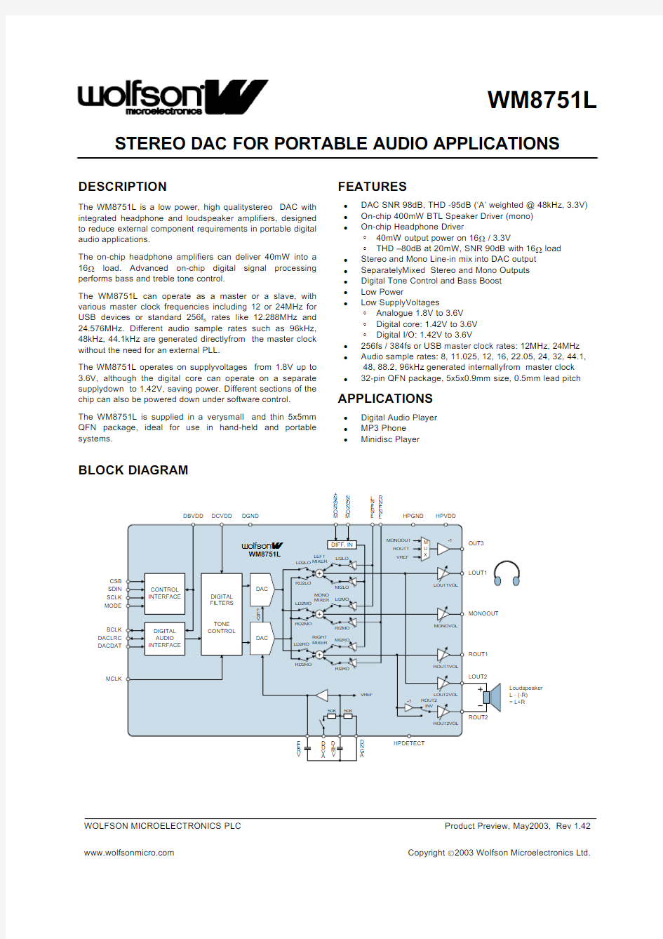
The WM8751L is a low power,high qualitystereo DAC with integrated headphone and loudspeaker amplifiers,designed to reduce external component requirements in portable digital audio applications.
The on-chip headphone amplifiers can deliver 40mW into a 16?load.Advanced on-chip digital signal processing performs bass and treble tone control.
The WM8751L can operate as a master or a slave,with various master clock frequencies including 12or 24MHz for USB devices or standard 256f s rates like 12.288MHz and 24.576MHz.Different audio sample rates such as 96kHz,48kHz,44.1kHz are generated directlyfrom the master clock without the need for an external PLL.
The WM8751L operates on supplyvoltages from 1.8V up to 3.6V,although the digital core can operate on a separate supplydown to 1.42V,saving power.Different sections of the chip can also be powered down under software control.The WM8751L is supplied in a verysmall and thin 5x5mm QFN package,ideal for use in hand-held and portable systems.
FEATURES
?DAC SNR 98dB,THD -95dB (‘A’weighted @48kHz,3.3V)?On-chip 400mW BTL Speaker Driver (mono)?
On-chip Headphone Driver
°40mW output power on 16?/3.3V
°THD –80dB at 20mW,SNR 90dB with 16?load ?Stereo and Mono Line-in mix into DAC output ?SeparatelyMixed Stereo and Mono Outputs ?Digital Tone Control and Bass Boost ?Low Power
?
Low SupplyVoltages
°Analogue 1.8V to 3.6V °Digital core:1.42V to 3.6V °Digital I/O:1.42V to 3.6V
?256fs /384fs or USB master clock rates:12MHz,24MHz ?Audio sample rates:8,11.025,12,16,22.05,24,32,44.1,48,88.2,96kHz generated internallyfrom master clock ?
32-pin QFN package,5x5x0.9mm size,0.5mm lead pitch
APPLICATIONS
?Digital Audio Player ?MP3Phone ?
Minidisc Player
BLOCK DIAGRAM
DCVDD DBVDD DGND BCLK DACDAT
DACLRC L I N E I N L L I N E I N R
CSB SDIN SCLK MODE
HPVDD
HPGND M O N O I N +
M O N O I N -MCLK
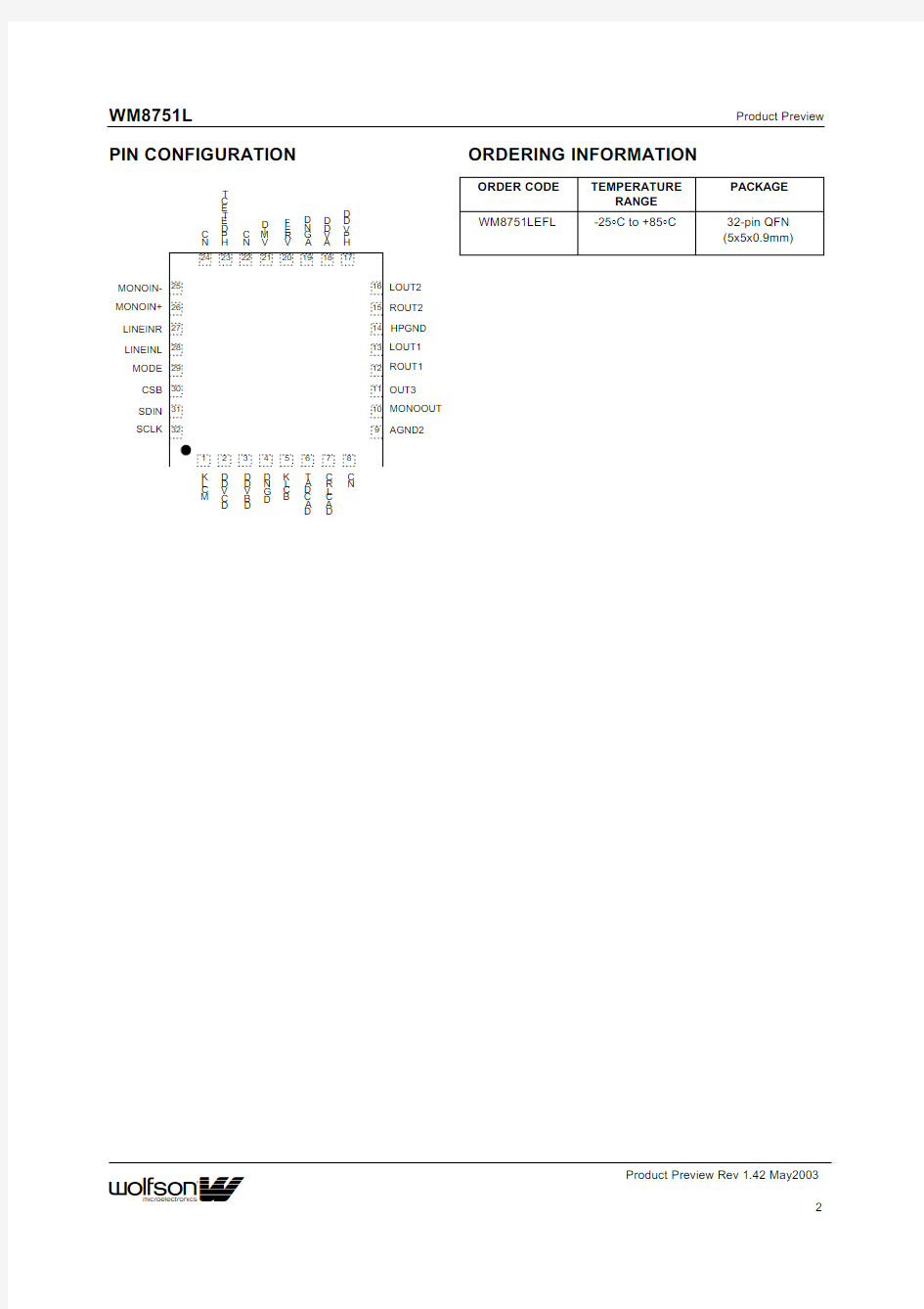
WM8751L Product Preview PIN CONFIGURATION ORDERING INFORMATION
ORDER CODE TEMPERATURE
RANGE
PACKAGE
WM8751LEFL-25°C to+85°C32-pin QFN
(5x5x0.9mm)
D
A
C
D
A
T
B
C
L
K
D
C
V
D
D
D
G
N
D
D
B
V
D
D
M
C
L
K
D
A
C
L
R
C
OUT3
A
V
D
D
V
M
I
D
A
G
N
D
V
R
E
F
N
C
H
P
D
E
T
E
C
T
HPGND
AGND2
MONOOUT
H
P
V
D
D
ROUT1
LOUT1
ROUT2
LOUT2
N
C
CSB
MODE
MONOIN+
LINEINL
LINEINR
MONOIN-
SDIN
SCLK
N
C
Product Preview WM8751L PIN DESCRIPTION
PIN#NAME TYPE DESCRIPTION
1MCLK Digital Input Master Clock
2DCVDD SupplyDigital Core Supply
3DBVDD SupplyDigital Buffer(I/O)Supply
4DGND SupplyDigital Ground(return path for both DCVDD and DBVDD)
5BCLK Digital Input/Output Audio Interface Bit Clock
6DACDAT Digital Input DAC Digital Audio Data
7DACLRC Digital Input/Output Audio Interface Left/Right Clock
8NC No Connect No Internal Connection
connected to AGND.Leave this pin floating or connect to 9AGND2SupplyInternally
AGND.
10MONOOUT Analogue Output Mono Output
11OUT3Analogue Output Output3(can be used as Headphone Pseudo Ground)
12ROUT1Analogue Output Right Output1(Line or Headphone)
13LOUT1Analogue Output Left Output1(Line or Headphone)
for Analogue Output Drivers(LOUT1/2,ROUT1/2) 14HPGND SupplySupply
15ROUT2Analogue Output Right Output1(Line or Headphone or Speaker)
16LOUT2Analogue Output Left Output1(Line or Headphone or Speaker)
for Analogue Output Drivers(LOUT1/2,ROUT1/2,MONOUT) 17HPVDD SupplySupply
18AVDD SupplyAnalogue Supply
19AGND SupplyAnalogue Ground(return path for AVDD)
20VREF Analogue Output Reference Voltage Decoupling Capacitor
21VMID Analogue Output Midrail Voltage Decoupling Capacitor
22NC No Connect No Internal Connection
23HPDETECT Logic Input Headphone/Speaker switch(referred to AVDD)
24NC No Connect No Internal Connection
25MONOIN-Analogue Input Negative end of MONOIN+,for differential mono signals
26MONOIN+Analogue Input Analogue Line-in to mixers(mono channel)
27LINEINR Analogue Input Analogue Line-in to mixers(right channel)
28LINEINL Analogue Input Analogue Line-in to mixers(left channel)
29MODE Digital Input Control Interface Selection
30CSB Digital Input Chip Select/Device Address Selection
31SDIN Digital Input/Output Control Interface Data Input/2-wire Acknowledge output
32SCLK Digital Input Control Interface Clock Input
WM8751L Product Preview ABSOLUTE MAXIMUM RATINGS
Absolute Maximum Ratings are stress ratings only.Permanent damage to the device maybe caused bycontinuously
operating at or beyond these limits.Device functional operating limits and guaranteed performance specifications are given
under Electrical Characteristics at the test conditions specified.
E SD Sensitive Device.This device is manufactured on a CMOS process.It is therefore genericallysusceptible
to damage from excessive static voltages.Proper ESD precautions must be taken during handling and storage
of this device.
CONDITION MIN MAX Supplyvoltages-0.3V+3.63V
Voltage range digital inputs DGND-0.3V DBVDD+0.3V Voltage range analogue inputs AGND-0.3V AVDD+0.3V Operating temperature range,T A-25°C+85°C
Storage temperature prior to soldering30°C max/85%RH max
Storage temperature after soldering-65°C+150°C Package bodytemperature(soldering10seconds)+260°C Package bodytemperature(soldering2minutes)+183°C
Notes
1.Analogue and digital grounds must always be within0.3V of each other.
2.All digital and analogue supplies are completelyindependent from each other.
RECOMMENDED OPERATING CONDITIONS
PARAMETER SYMBOL TEST CONDITIONS MIN TYP MAX UNIT Digital supplyrange(Core)DCVDD 1.42 2.0 3.6V Digital supplyrange(Buffer)DBVDD 1.8 2.0 3.6V Analogue supplies range AVDD,HPVDD 1.8 2.0 3.6V Ground DGND,AGND,HPGND0V
Product Preview
WM8751L
ELECTRICAL CHARACTERISTICS
Test Conditions
DCVDD =1.5V,AVDD =HPVDD =3.3V,T A =+25o C,1kHz signal,fs =48kHz,24-bit audio data unless otherwise stated.PARAMETER SYMBOL TEST CONDITIONS MIN
TYP MAX
UNIT DAC to Line-Out (LOUT1/2,ROUT1/2,MONOOUT with 10k ?/50pF load)
AVDD =3.3V 98Signal to Noise Ratio (A-weighted)
SNR AVDD =1.8V 95dB
AVDD =3.3V -95Total Harmonic Distortion THD
AVDD =1.8V -90dB
Channel Separation 1kHz signal 90
dB Analogue Mixer Inputs (LINEINL,LINEINR,MONOIN+)
AVDD =3.3V 1.0Full-scale Input Signal Level V INFS AVDD =1.8V 0.516V rms
AVDD =3.3V 95Signal to Noise Ratio Line-in to Line-Out (A-weighted)
SNR AVDD =1.8V
90dB AVDD =3.3V -92dB Total Harmonic Distortion THD AVDD =1.8V -92dB PGA gain =0dB 20Input Resistance
(signal enters one mixer only)PGA gain =+6dB 10PGA gain =0dB 10Input Resistance
(signal enters two mixers)R LINEIN
PGA gain =+6dB
5k ?MONOIN-input resistance R MONOIN-anygain
20
k ?Programmable Gain
-15
+6
dB Programmable Gain Step Size Monotonic
3dB Mute Attenuation
TBD
dB Analogue Outputs (LOUT1/2,ROUT1/2,MONOOUT)0dB Full scale output voltage AVDD/3.3
Vrms Programmable Gain 1kHz signal -67
+6
dB Programmable Gain Steps Monotonic 80steps Mute attenuation 1kHz,full scale signal
85dB Channel Separation
8090dB
Headphone Output (LOUT1/2,ROUT1/2with 16or 32Ohm load)Output Power per channel P O Output power is verycloselycorrelated with THD;see below.
HPVDD=1.8V,R L =32?
P O =5mW 0.013-78HPVDD=1.8V,R L =16?
P O =5mW 0.013-78HPVDD=3.3V,R L =32?,
P O =20mW 0.01-80Total Harmonic Distortion
THD
HPVDD=3.3V,R L =16?,
P O =20mW
0.01-80dB %
HPVDD =3.3V 90Signal to Noise Ratio (A-weighted)
SNR
HPVDD =1.8V
90
dB
WM8751L
Product Preview
Test Conditions
DCVDD =1.5V,AVDD =HPVDD =3.3V,T A =+25o C,1kHz signal,fs =48kHz,24-bit audio data unless otherwise stated.PARAMETER SYMBOL
TEST CONDITIONS MIN
TYP MAX
UNIT Speaker Output (LOUT2/ROUT2with 8?bridge tied load,ROUT2INV=1)
HPVDD=3.3V,R L =8?400HPVDD=3.0V,R L =8?300Output Power
P O
HPVDD=2.7V,R L =8?
230mW
HPVDD=3.3V,R L =8?75HPVDD=3.0V,R L =8?75Signal to Noise Ratio (A-weighted)
SNR
HPVDD=2.7V,R L =8?
75dB
Po=150mW,R L =8?,
HPVDD=3.3V -600.1Total Harmonic Distortion
THD
Po=300mW,R L =8?HPVDD=3.3V
-500.3
dB %Analogue Reference Levels Midrail Reference Voltage VMID –3%AVDD/2+3%V Buffered Reference Voltage VREF –3%
AVDD/2
+3%V VREF source current I VREF 5mA VREF sink current I VREF
5
mA
Digital Input /Output Input HIGH Level V IH 0.7×DBVDD
V Input LOW Level V IL 0.3×DBVDD
V Output HIGH Level V OH 0.9×DBVDD
V Output LOW Level
V OL
0.1×DBVDD
V
TERMINOLOGY
1.Signal-to-noise ratio (dB)-SNR is a measure of the difference in level between the full scale output and the output with no signal applied.(No Auto-zero or Automute function is employed in achieving these results).
2.
Dynamic range (dB)-DR is a measure of the difference between the highest and lowest portions of a signal.Normallya THD+N measurement at 60dB below full scale.The measured signal is then corrected byadding the 60dB to it.(e.g.THD+N @-60dB=-32dB,DR=92dB).
3.THD+N (dB)-THD+N is a ratio,of the rms values,of (Noise +Distortion)/Signal.
4.
Channel Separation (dB)-Also known as Cross-Talk.This is a measure of the amount one channel is isolated from the other.Normallymeasured bysending a full scale signal down one channel and measuring the other.
Product Preview
WM8751L
OUTPUT PGA’S LINEARITY
-70.000
-60.000-50.000-40.000-30.000-20.000-10.0000.000
10.00040
50
60
70
80
90
100
110
120
130
XXXVOL Register Setting (binary)
M e a s u r e d G a i n [d B ]
0.000
0.2500.5000.750
1.0001.2501.5001.750
2.00040
50
60
70
80
90
100
110
120
130
XXXVOL Register Setting (binary)
S t e p S i z e [d B ]
WM8751L
Product Preview
HEADPHONE OUTPUT THD VERSUS POWER (SIMULATION)
-100
-80
-60
-40
-20
5
10
1520
25
30
Pow er (mW)
T H D +N (d B )
-100
-80
-60
-40
-20
10
20
3040
50
60
Pow er (mW)
T H D +N (d B )
Product Preview
WM8751L
SPEAKER OUTPUT THD VERSUS POWER (SIMULATION)
Speaker Pow er vs THD+N (8Ohm BTL load)
-70
-60-50-40-30
-20-100
100
200
300
400
500
Pow er (mW)
T H D +N (d B )
Speaker Power vs THD+N (8Ohm BTL load)
02
4
6
8
10
100
200
300
400
500
Power (mW)
T H D +N (%)
WM8751L Product Preview POWER CONSUMPTION
The power consumption of the WM8751L depends on the following factors.
?Supplyvoltages:Reducing the supplyvoltages also reduces supplycurrents,and therefore results in significant power savings.
?Operating mode:Power consumption is lower in mono modes than in stereo,as one DAC is switched OFF.Unused analogue outputs should be switched off.
Table1Supply Current Consumption(Target)
Notes:
1.T A=+25o C,Slave Mode,fs=48kHz,MCLK=1
2.288MHz(256fs),24-bit data
2.All figures are quiescent,with no signal.
3.The power dissipated in the headphone itself is not included in the above table.
Product Preview
WM8751L
SIGNAL TIMING REQUIREMENTS
SYSTEM CLOCK TIMING
Figure 1System Clock Timing Requirements Test Conditions
DBVDD =3.3V,DGND =0V,T A =+25o C,Slave Mode fs =48kHz,MCLK =256fs,24-bit data,unless otherwise stated.PARAMETER
SYMBOL MIN TYP MAX UNIT System Clock Timing
Information
MCLK System clock pulse width high t MCLKL 16ns MCLK System clock pulse width low t MCLKH 16ns MCLK System clock cycle time
t MCLKY
27
ns
AUDIO INTERFACE TIMING –MASTER MODE
Figure 2Digital Audio Data Timing –Master Mode (see Control Interface)Test Conditions
DBVDD =3.3V,DGND =0V,T A =+25o C,Slave Mode fs =48kHz,MCLK =256fs,24-bit data,unless otherwise stated.PARAMETER
SYMBOL MIN TYP MAX UNIT System Clock Timing
Information
DACLRC propagation delayfrom BCLK falling edge t DL 10
ns DACDAT setup time to BCLK rising edge t DST 10ns DACDAT hold time from BCLK rising edge
t DHT
10
ns
AUDIO INTERFACE TIMING –SLAVE MODE
Figure 3Digital Audio Data Timing –Slave Mode (see Control Interface)
WM8751L
Product Preview
Test Conditions
DBVDD =3.3V,DGND =0V,T A =+25o C,Slave Mode fs =48kHz,MCLK =256fs,24-bit data,unless otherwise stated.PARAMETER
SYMBOL MIN TYP MAX UNIT System Clock Timing Information
BCLK cycle time t BCY 50ns BCLK
pulse width high t BCH 20ns BCLK pulse width low
t BCL 20ns DACLRC setup time to BCLK rising edge t LRSU 10ns DACLRC hold time from BCLK rising edge t LRH 10ns DACDAT hold time from BCLK rising edge
t DH
10
ns
CONTROL INTERFACE TIMING –3-WIRE MODE
Figure 4Control Interface Timing –3-Wire Serial Control Mode Test Conditions
DBVDD =3.3V,DGND =0V,T A =+25o C,Slave Mode,fs =48kHz,MCLK =256fs,24-bit data,unless otherwise stated.PARAMETER
SYMBOL
MIN
TYP
MAX
UNIT
Program Register Input Information SCLK rising edge to CSB rising edge t SCS 500ns SCLK pulse cycle time t SCY 200ns SCLK pulse width low t SCL 80ns SCLK pulse width high t SCH 80ns SDIN to SCLK set-up time t DSU 40ns SCLK to SDIN hold time t DHO 40ns CSB pulse width low t CSL 40ns CSB pulse width high t CSH 40ns CSB rising to SCLK rising
t CSS 40ns Pulse width of spikes that will be suppressed
t ps
5
ns
Product Preview WM8751L CONTROL INTERFACE TIMING–2-WIRE MODE
Figure5Control Interface Timing–2-Wire Serial Control Mode
Test Conditions
DBVDD=3.3V,DGND=0V,T A=+25o C,Slave Mode,fs=48kHz,MCLK=256fs,24-bit data,unless otherwise stated.
PARAMETER SYMBOL MIN TYP MAX UNIT Program Register Input Information
SCLK Frequency0400kHz SCLK Low Pulse-Width t1600ns SCLK High Pulse-Width t2 1.3us Hold Time(Start Condition)t3600ns Setup Time(Start Condition)t4600ns Data Setup Time t5100ns SDIN,SCLK Rise Time t6300ns SDIN,SCLK Fall Time t7300ns Setup Time(Stop Condition)t8600ns Data Hold Time t9900ns Pulse width of spikes that will be suppressed t ps05ns
WM8751L Product Preview DEVICE DESCRIPTION
INTRODUCTION
The WM8751L is a low power audio DAC offering a combination of high qualityaudio,advanced
features,low power and small size.These characteristics make it ideal for portable digital audio
applications such as portable music players and smartphones.
The device has a configurable digital audio interface where digital audio data is fed to the internal
digital filters and then the DAC.The interface supports a number of audio data formats including I2S,
DSP Mode(a burst mode in which frame sync plus2data packed words are transmitted),Left
Justified and Right Justified formats,and can operate in master or slave modes.
The on-chip digital filters perform tone control and digital volume control according to the user
setting,and convert the audio data into oversampled bitstreams,which are passed to the left and
right channel DACs.A multi-bit,low-orderΣ?DAC architecture with dynamic element matching is
used,delivering optimum performance with low power consumption.
The DAC output signal enters an analogue mixer where analogue input signals can be added to it.
The WM8751L has a total of six analogue output pins,which can be configured as stereo line-outs,
mono line-outs,differential mono line-outs,stereo headphone outputs or differential mono(BTL)
speaker outputs.
The WM8751L master clock can be either an industrystandard256/384f s clock or a12MHz/24MHz
USB clock.Sample rates of8kHz,11.025kHz,12kHz,16kHz,22.05kHz,32kHz,44.1kHz,48kHz,
88.2kHz and96kHz can be generated directlyfrom the master clock,without an external PLL.The
digital filters are optimised for each sample rate.
To allow full software control over all its features,the WM8751L offers a choice of2or3wire MPU
control interface.It is fullycompatible and an ideal partner for a wide range of industrystandard
microprocessors,controllers and DSPs.
The design of the WM8751L has given much attention to power consumption without compromising
performance.It operates at verylow voltages,and includes the abilityto power off parts of the
circuitryunder software control,including standbyand power off modes.
Product Preview WM8751L SIGNAL PATH
The WM8751L signal paths consists of digital filters,DACs,analogue mixers and output drivers.
E ach circuit block can be enabled or disabled separatelyusing the control bits in register26(see
“Power Management”).Thus it is possible to utilise the analogue mixing and amplification provided
bythe WM8751L,irrespective of whether the DACs are running or not.
The WM8751L receives digital input data on the DACDAT pin.The digital filter block processes the
data to provide the following functions:
?Digital volume control
?Tone control and Bass Boost
?Digital Mono Mix
?Sigma-Delta Modulation
Two high performance,sigma-delta audio DACs convert the digital data into two analogue signals
(left and right).These can then be mixed with analogue signals from the LINEINL,LINEINR and
MONOIN pins,and the mix is fed to the output drivers,LOUT1/ROUT1,LOUT2/ROUT2,and
MONOOUT.
?LOUT1/ROUT1:can drive16?or32?stereo headphones or stereo line output.
?LOUT2/ROUT2:can drive an8?mono speaker,stereo headphones or a stereo line-out.
?MONOOUT:line output designed to drive a10k?load.
?OUT3:multi-function output,maybe used for capacitor-less headphone drive,differential
mono-out,line-out or32?earpiece driver.
WM8751L Product Preview DIGITAL VOLUME CONTROL
The WM8751L has on-chip digital attenuation from–127dB to0dB in0.5dB steps,allowing the user
to adjust the volume of each channel separately.The level of attenuation for an eight-bit code X is
given by:
-0.5×(255–X)dB for1≤X≤255;MUTE for X=0
The LDVU and RDVU control bits control the loading of digital volume control data.When LDVU or
RDVU are set to0,the LDACVOL or RDACVOL control data is loaded into an intermediate register,
but the actual gain does not change.Both left and right gain settings are updated simultaneously
when either LDVU or RDVU are set to1.
REGISTER
ADDRESS
BIT LABEL DEFAULT DESCRIPTION
7:0LDACVOL[7:0]11111111
(0dB)Left DAC Digital Volume Control 00000000=Digital Mute 00000001=-127dB 00000010=-126.5dB
...0.5dB steps up to 11111111=0dB
R10(0Ah)
Left Channel
Digital Volume
8LDVU0Left DAC Volume Update
0=Store LDACVOL in intermediate latch
(no gain change)
1=Update left and right channel gains
(left=LDACVOL,right=intermediate
latch)
7:0RDACVOL[7:0]11111111
(0dB)Right DAC Digital Volume Control similar to LDACVOL
R11(0Bh)
Right Channel
Digital Volume8RDVU0Right DAC Volume Update
0=Store RDACVOL in intermediate latch
(no gain change)
1=Update left and right channel gains
(left=intermediate latch,right=
RDACVOL)
Table2Digital Volume Control
Product Preview
WM8751L
TONE CONTROL
The WM8751L provides separate controls for bass and treble with programmable gains and filter characteristics.This function operates on digital audio data before it is passed to the audio DACs.Bass control can take two different forms:?
Linear bass control:bass signals are amplified or attenuated bya user programmable gain.This is independent of signal volume,and veryhigh bass gains on loud signals maylead to signal clipping.
?
Adaptive bass boost:The bass volume is amplified bya variable gain.When the bass volume is low,it is boosted more than when the bass volume is high.This method is recommended because it prevents clipping,and usuallysounds more pleasant to the human ear.
Treble control applies a user programmable gain,without anyadaptive boost function.
REGISTER ADDRESS BIT LABEL DEFAULT
DESCRIPTION
7
BB
Bass Mode
0=Linear bass control 1=Adaptive bass boost
6BC 0
Bass Filter Characteristic
0=Low Cutoff (130Hz at 48kHz sampling)1=High Cutoff (200Hz at 48kHz sampling)Bass Intensity Code BB=0BB=10000+9dB 15(max)0001+9dB 140010+7.5dB 13…(1.5dB steps)…01110dB
8…(1.5dB steps)…1011-1101-6dB 4-21110-6dB
1(min)
R12(0Ch)Bass Control
3:0BASS 1111(OFF)
1111
Bypass (OFF)
6
TC
Treble Filter Characteristic
0=High Cutoff (8kHz at 48kHz sampling)1=Low Cutoff (4kHz at 48kHz sampling)R13(0Dh)Treble Control
3:0TRBL
1111
(Disabled)
Treble Intensity
0000or 0001=+9dB 0010=+7.5dB …(1.5dB steps)1011to 1110=-6dB 1111=Disable
Table 3Tone Control Note:1.
All cut-off frequencies change proportionallywith the DAC sample rate.
WM8751L
Product Preview
DIGITAL TO ANALOGUE CONVERTER (DAC)
Treble and linear bass enhancement mayproduce signals that exceed full-scale.In order to avoid limiting under these conditions,it is recommended to set the DAT bit to attenuate the digital input signal by6dB.The gain at the outputs should be increased by6dB to compensate for the attenuation.Cut-onlytone adjustment and adaptive bass boost cannot produce signals above full-scale and therefore do not require the DAT bit to be set.
After passing through the tone control filters,digital ‘de-emphasis’can be applied to the audio data if necessary(e.g.when the data comes from a CD with pre-emphasis used in the recording).De-emphasis filtering is available for sample rates of 48kHz,44.1kHz and 32kHz.
The WM8751L also has a Soft Mute function,which graduallyattenuates the volume of the digital signal to zero.This function is enabled bydefault.To playback an audio signal,the WM8751L must first be unmuted bysetting the DACMU bit to zero.
REGISTER ADDRESS BIT LABEL DEFAULT
DESCRIPTION
7
DAT
DAC 6dB attenuate enable 0=disabled (0dB)1=-6dB enabled
3DACMU 1
DAC Digital Soft Mute 1=mute
0=no mute (signal active)R5(05h)DAC Control
2:1DEEMPH 00
De-emphasis Control 11=48kHz sample rate 10=44.1kHz sample rate 01=32kHz sample rate 00=No De-emphasis
Table 4DAC Control
The digital audio data is converted to oversampled bit streams in the on-chip,true 24-bit digital interpolation filters.The bitstream data enters two multi-bit,sigma-delta DACs,which convert them to high qualityanalogue audio signals.The multi-bit DAC architecture reduces high frequencynoise and sensitivityto clock jitter.It also uses a Dy namic E lement Matching technique for high linearityand low distortion.
In normal operation,the left and right channel digital audio data are converted to analogue in two separate DACs.However,it is also possible to disable one channel,so that the same signal (left or right)appears on both analogue output channels.Additionally,there is a mono-mix mode where the two audio channels are mixed together digitallyand then converted to analogue using onlyone DAC,while the other DAC is switched off.The mono-mix signal can be selected to appear on both analogue output channels (see Analogue Outputs).
REGISTER ADDRESS BIT LABEL DEFAULT
DESCRIPTION
R23(17h)Additional (1)
5:4
DMONOMIX[1:0]
00
DAC mono mix 00:stereo
01:mono ((L+R)/2)into DACL,‘0’into DACR
10:mono ((L+R)/2)into DACR,‘0’into DACL
11:mono ((L+R)/2)into DACL &DACR
Table 5DAC Mono Mix Select
Product Preview
WM8751L
LINE INPUTS AND OUTPUT MIXERS
The WM8751L provides the option to mix the DAC output signal with analogue line-in signals from the LINEINL,LINEINR and MONOIN pins.The level of the mixed-in signals can be controlled with PGAs (Programmable Gain Amplifiers).
LINEINL,LINEINR,MONOIN+and MONOIN-are high impedance,low capacitance AC coupled analogue inputs.Theyare biased internallyto the reference voltage VRE F.Whenever these inputs are muted or the device placed into standbymode,the inputs remain biased to VRE F using special anti-thump circuitry.This reduces any audible clicks that may otherwise be heard when re-activating the inputs.
REGISTER ADDRESS BIT LABEL DEFAULT DESCRIPTION
8
LD2LO
Left DAC to Left Mixer 0=Disable (Mute)1=Enable Path
7LI2LO 0
LINEINL Signal to Left Mixer 0=Disable (Mute)1=Enable Path
R34(22h)Left Mixer (1)
6:4LI2LOVOL
101(-9dB)
LINEINL Signal to Left Mixer Volume 000=+6dB …(3dB steps)111=-15dB
8RD2LO 0
Right DAC to Left Mixer 0=Disable (Mute)1=Enable Path
7MI2LO 0
MONOIN Signal to Left Mixer 0=Disable (Mute)1=Enable Path
R35(23h)Left Mixer (2)
6:4MI2LOVOL
101(-9dB)
MONOIN Signal to Left Mixer Volume 000=+6dB …(3dB steps)111=-15dB
Table 6Left Output Mixer Control
WM8751L
Product Preview
REGISTER ADDRESS BIT LABEL DEFAULT
DESCRIPTION
8
LD2RO
Left DAC to Right Mixer 0=Disable (Mute)1=Enable Path
7MI2RO 0
MONOIN Signal to Right Mixer 0=Disable (Mute)1=Enable Path
R36(24h)
Right Mixer (1)
6:4MI2ROVOL
101(-9dB)
MONOIN Signal to Right Mixer Volume 000=+6dB …(3dB steps)111=-15dB
8RD2RO 0
Right DAC to Right Mixer 0=Disable (Mute)1=Enable Path
7RI2RO 0
LINEINR Signal to Right Mixer 0=Disable (Mute)1=Enable Path
R37(25h)
Right Mixer (2)
6:4RI2ROVOL
101(-9dB)
LINEINR Signal to Right Mixer Volume 000=+6dB …(3dB steps)111=-15dB
Table 7Right Output Mixer Control
REGISTER ADDRESS BIT LABEL DEFAULT DESCRIPTION
8
LD2MO
Left DAC to Mono Mixer 0=Disable (Mute)1=Enable Path
7LI2MO 0
LINEINL Signal to Mono Mixer 0=Disable (Mute)1=Enable Path
R38(26h)
Mono Mixer (1)
6:4LI2MOVOL
101(-9dB)
LINEINL Signal to Right Mono Volume 000=0dB …(3dB steps)111=-21dB
8RD2MO 0
Right DAC to Mono Mixer 0=Disable (Mute)1=Enable Path
7RI2MO 0
LINEINR Signal to Mono Mixer 0=Disable (Mute)1=Enable Path
R39(27h)
Mono Mixer (2)
6:4RI2MOVOL
101(-9dB)
LINEINR Signal to Mono Mixer Volume 000=0dB …(3dB steps)111=-21dB
Table 8Mono Output Mixer Control
Note:The mono mixer has half the gain of the left and right mixers (i.e.6dB less),to ensure that the left and right channels can be mixed to mono without clipping.