General Description
The DS1086L EconOscillator? is a 3.3V programmable clock generator that produces a spread-spectrum (dithered) square-wave output of frequencies from 130kHz to 66.6MHz. The selectable dithered output reduces radiated-emission peaks by dithering the fre-quency 0.5%,1%, 2%, 4%, or 8% below the pro-grammed frequency. The DS1086L has a power-down mode and an output-enable control for power-sensitive applications. All the device settings are stored in non-volatile (NV) EEPROM memory allowing it to operate in stand-alone applications.
Applications
Printers Copiers PCs
Computer Peripherals Cell Phones Cable Modems
Features
?User-Programmable Square-Wave Generator ?Frequencies Programmable from 130kHz to 66.6MHz ?0.5%, 1%, 2%, 4%, or 8% Selectable Dithered Output ?Adjustable Dither Rate
?Glitchless Output-Enable Control ?2-Wire Serial Interface ?Nonvolatile Settings ?2.7V to 3.6V Supply
?No External Timing Components Required ?Power-Down Mode
?5kHz Master Frequency Step Size ?EMI Reduction
?Industrial Temperature Range: -40°C to +85°C
DS1086L
3.3V Spread-Spectrum EconOscillator
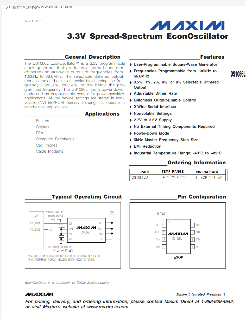
Pin Configuration
Ordering Information
Typical Operating Circuit
Rev 1; 9/07
EconOscillator is a trademark of Dallas Semiconductor.
________________________________________________________________Maxim Integrated Products
1
For pricing, delivery, and ordering information, please contact Maxim Direct at 1-888-629-4642,or visit Maxim’s website at https://www.doczj.com/doc/01147012.html,.
D S 1086L
3.3V Spread-Spectrum EconOscillator 2_______________________________________________________________________________________
ABSOLUTE MAXIMUM RATINGS
RECOMMENDED DC OPERATING CONDITIONS
(V CC = 2.7V to 3.6V, T A = -40°C to +85°C.)
Stresses beyond those listed under “Absolute Maximum Ratings” may cause permanent damage to the device. These are stress ratings only, and functional operation of the device at these or any other conditions beyond those indicated in the operational sections of the specifications is not implied. Exposure to absolute maximum rating conditions for extended periods may affect device reliability.
DC ELECTRICAL CHARACTERISTICS
Voltage Range on V CC Relative to Ground ..........-0.5V to +6.0V Voltage Range on SPRD, PDN , OE, SDA, and SCL
Relative to Ground*..................................-0.5 to (V CC + 0.5V)Operating Temperature Range ...........................-40°C to +85°C Programming Temperature Range.........................0°C to +70°C Storage Temperature Range.............................-55°C to +125°C Soldering Temperature ..................See IPC/JEDEC J-STD-020A
*This voltage must not exceed 6.0V.
DS1086L
3.3V Spread-Spectrum EconOscillator
_______________________________________________________________________________________3
MASTER OSCILLATOR CHARACTERISTICS
D S 1086L
3.3V Spread-Spectrum EconOscillator 4_______________________________________________________________________________________
AC ELECTRICAL CHARACTERISTICS
AC ELECTRICAL CHARACTERISTICS—2-WIRE INTERFACE
DS1086L
3.3V Spread-Spectrum EconOscillator
_______________________________________________________________________________________5
AC ELECTRICAL CHARACTERISTICS—2-WIRE INTERFACE (continued)
NONVOLATILE MEMORY CHARACTERISTICS
(V CC = 2.7V to 3.6V)Note 1:All voltages are referenced to ground.
Note 2:DAC and OFFSET register settings must be configured to maintain the master oscillator frequency within this range.Correct operation of the device is not guaranteed if these limits are exceeded.
Note 3:This is the absolute accuracy of the master oscillator frequency at the default settings.
Note 4:This is the change that is observed in master oscillator frequency with changes in voltage from nominal voltage at T A = +25°C.
Note 5:
This is the percentage frequency change from the +25°C frequency due to temperature at V CC = 3.3V.The maximum temper-ature change varies with the master oscillator frequency setting. The minimum occurs at the default master oscillator frequen-cy (f default ). The maximum occurs at the extremes of the master oscillator frequency range (33.3MHz or 66.6MHz). Note 6:The dither deviation of the master oscillator frequency is unidirectional and lower than the undithered frequency.
Note 7:The integral nonlinearity of the frequency is a measure of the deviation from a straight line drawn between the two end-points (f osc(MIN)to f osc(MAX)) of the range. The error is in percentage of the span.Note 8:This is true when the prescaler = 1.
Note 9:Frequency settles faster for small changes in value. During a change, the frequency transitions smoothly from the original value to the new value.
Note 10:
This indicates the time elapsed between power-up and the output becoming active. An on-chip delay is intentionally introduced to allow the oscillator to stabilize. t stab is equivalent to approximately 512 master clock cycles and therefore depends on the programmed clock frequency.
Note 11:Output voltage swings can be impaired at high frequencies combined with high output loading.
Note 12:
A fast-mode device can be used in a standard-mode system, but the requirement t SU:DAT > 250ns must then be met.This is automatically the case if the device does not stretch the LOW period of the SCL signal. If such a device does stretch the LOW period of the SCL signal, it must output the next data bit to the SDA line at least t R MAX + t SU:DAT =1000ns + 250ns = 1250ns before the SCL line is released.Note 13:After this period, the first clock pulse is generated.
Note 14: A device must internally provide a hold time of at least 300ns for the SDA signal (referred to as the V IH MIN of the SCL signal) to bridge the undefined region of the falling edge of SCL.
Note 15:The maximum t HD:DAT need only be met if the device does not stretch the LOW period (t LOW ) of the SCL signal.Note 16:C B —total capacitance of one bus line, timing referenced to 0.9 x V CC and 0.1 x V CC .
Note 17:
Typical frequency shift due to aging is ±0.5%. Aging stressing includes Level 1 moisture reflow preconditioning (24hr +125°C bake, 168hr 85°C/85%RH moisture soak, and three solder reflow passes +240 +0/-5°C peak) followed by 1000hr max V CC biased 125°C HTOL, 1000 temperature cycles at -55°C to +125°C, 96hr 130°C/85%RH/3.6V HAST and 168hr 121°C/2 ATM Steam/Unbiased Autoclave.
Note 18:
t stab is the time required after exiting power-down to the beginning of output oscillations. In addition, a delay of t DACstab is required before the frequency will be within its specified tolerance.
Typical Operating Characteristics
(V CC = 3.3V, T A = 25°C, unless otherwise noted.)
D S 1086L
3.3V Spread-Spectrum EconOscillator 6_______________________________________________________________________________________
SUPPLY CURRENT vs.
MASTER OSCILLATOR FREQUENCY
MASTER FREQUENCY (MHz)
S U P P L Y C U R R E N T (m A )
63603639424851544557234567891
3366
SUPPLY CURRENT vs. TEMPERATURE
TEMPERATURE (°C)
S U P P L Y C U R R E N T (m A )
60
35
10
-15
4
5678
9103-40
85
SUPPLY CURRENT vs. PRESCALER
PRESCALER
S U P P L Y C U R R E N T (m A )
100
10
123456701
1000
MASTER OSCILLATOR FREQUENCY PERCENT
CHANGE vs. SUPPLY VOLTAGE
SUPPLY VOLTAGE (V)P E R C E N T C H A N G E T (%)
3.3
3.0
-0.4-0.3-0.2-0.100.10.20.30.40.5-0.5
2.7
3.6
MASTER OSCILLATOR FREQUENCY PERCENT
CHANGE vs. TEMPERATURE
TEMPERATURE (°C)P E R C E N T C H A N G E (%)
60
35
-15
10
-1.25-1.00-0.75-0.500
-0.250.250.50-1.50
-40
85
DUTY CYCLE vs. TEMPERATURE
TEMPERATURE (°C)
D U T Y C Y C L
E (%)
60
35
10
-15
51
52
53
5455
50-40
85
DUTY CYCLE vs. SUPPLY VOLTAGE
SUPPLY VOLTAGE (V)
3.3
3.0
2.7
3.6
D U T Y C Y C L
E (%)
51
5253
5455
DS1086L
3.3V Spread-Spectrum EconOscillator
POWER-DOWN CURRENT vs. TEMPERATURE
D S 1086L t o c 09
TEMPERATURE (°C)
P O W E R -D O W N C U R R E N T (μA )
603510-151.461.481.501.521.541.561.581.60
1.621.64
1.44
-4085
SUPPLY CURRENT WITH OUTPUT DISABLED vs. SUPPLY VOLTAGE
SUPPLY VOLTAGE (V)
S U P P L Y C U R R E N T (m A )
3.3
3.0
0.51.01.52.02.53.0
3.5
4.002.7
3.6
SUPPLY CURRENT WITH OUTPUT DISABLED vs. TEMPERATURE
SUPPLY VOLTAGE (V)
S U P P L Y C U R R E N T (m A )
60
35
10
-15
2.3
2.4
2.5
2.62.7
2.2
-40
85
Typical Operating Characteristics (continued)
(V CC = 3.3V, T A = 25°C, unless otherwise noted.)
_______________________________________________________________________________________7
POWER-DOWN CURRENT vs.
SUPPLY VOLTAGE
SUPPLY VOLTAGE (V)P O W E R -D O W N C U R R E N T (μA )
3.0
3.3
1.11.21.31.41.61.51.71.81.0
2.7
3.6
D S 1086L
3.3V Spread-Spectrum EconOscillator 8
DS1086L
3.3V Spread-Spectrum EconOscillator
_______________________________________________________________________________________
9
Detailed Description
A block diagram of the DS1086L is shown in Figure 3.The internal master oscillator generates a square wave with a 33.3MHz to 66.6MHz frequency range. The fre-quency of the master oscillator can be programmed with the DAC register over a two-to-one range in 5kHz steps. The master oscillator range is larger than the range possible with the DAC step size, so the OFFSET register is used to select a smaller range of frequencies over which the DAC spans. The prescaler can then be set to divide the master oscillator frequency by 2x (where x equals 0 to 8) before routing the signal to the output (OUT) pin.
A programmable triangle-wave generator injects an off-set element into the master oscillator to dither its output 0.5%, 1%, 2%, 4%, or 8%. The dither magnitude is con-trolled by the JS2, JS1, and JS0 bits in the PRESCALER word and enabled with the SPRD pin. Futhermore, the dither rate is controlled by the JS4 and JS3 bits in the PRESCALER word and determines the frequency of the dither. The maximum spectral attenuation occurs when the prescaler is set to 1 and is reduced by 2.7d
B for every factor of 2 that is used in the prescaler. This hap-
pens because the prescaler’s divider function tends to average the dither in creating the lower frequency.However, the most stringent spectral emission limits are imposed on the higher frequencies where the prescaler is set to a low divider ratio.
The external control input, OE, gates the clock output buffer. The PDN pin disables the master oscillator and turns off the clock output for power-sensitive applica-tions*. On power-up, the clock output is disabled until power is stable and the master oscillator has generated 512 clock cycles. Both controls feature a synchronous enable that ensures there are no output glitches when the output is enabled.
The control registers are programmed through a 2-wire interface and are used to determine the output frequen-cy and settings. Once programmed into EEPROM,since the register settings are NV, the settings only need to be reprogrammed if it is desired to reconfigure the device.
*The power-down command must persist for at least two out-put frequency cycles plus 10μs for deglitching purposes.
D S 1086L
3.3V Spread-Spectrum EconOscillator
10
______________________________________________________________________________________
The output frequency is determined by the following equation:
where: min frequency of selected OFFSET range is the lowest frequency (shown in Table 2 for the correspond-ing offset).
DAC value is the value of the DAC register (0 to 1023).Prescaler is the value of 2x where x = 0 to 8.
more in-depth look at using the registers.
________________Register Definitions
The DS1086L registers are used to program the output frequency, dither percent, dither rate, and 2-wire address. Table 1 shows a summary of the registers and detailed descriptions follow below.
PRESCALER (02h)
The PRESCALER word is a two-byte value containing control bits for the prescaler (P3 to P0), output control (Lo/HiZ ), the jitter rate (JS4 to JS3), as well as control bits for the jitter percentage (JS2 to JS0). The
PRESCALER word is read and written using two-byte reads and writes beginning at address 02h.JS4 to JS3:Jitter Rate . This is the frequency of the tri-angle wave generator and the modulation frequency that the output is dithered. It can be programmed to the master oscillator frequency, f OSC , divided by either
DS1086L
3.3V Spread-Spectrum EconOscillator
______________________________________________________________________________________
11
JS2 to JS0:Jitter Percentage . These three bits select the amount of jitter in percent. The SPRD pin must be a
state of the output pin when the device is in power-down mode or when the output is disabled. If Lo/HiZ =0, the output is HiZ when in power-down or disabled. If Lo/HiZ = 1, the output is held low when in power-down or disabled.
P3 to P0:Prescaler Divider.These bits divide the master oscillator frequency by 2x , where x is P3 to P0and can be from 0 to 8. Any prescaler value entered greater than 8 decodes as 8.
DAC (08h)
B9 to B0:DAC Setting.The DAC word sets the master oscillator frequency to a specific value within the cur-rent offset range. Each step of the DAC changes the master oscillator frequency by 5kHz. The DAC word is read and written using two-byte reads and writes beginning at address 08h.
OFFSET (0Eh)
B4 to B0:Offset.This value selects the master oscilla-tor frequency range that can be generated by varying the DAC word. Valid frequency ranges are shown in Table 2. Correct operation of the device is not guaran-teed for values of OFFSET not shown in the table.
The default offset value (OS) is factory trimmed and can vary from device to device. Therefore, to change frequency range, OS must be read so the new offset value can be calculated relative to the default. For example, to generate a master oscillator frequency within the largest range (61.4MHz to 66.6MHz), Table 2indicates that the OFFSET must be programmed to OS + 6. This is done by reading the RANG E register and adding 6 to the value of bits B4 to B0. The result is then written into bits B4 to B0 of the OFFSET register.Additional examples are provided in the Example Frequency Calculations section.
RANGE (37h)
B4 to B0:Range:This read-only, factory programmed value is a copy of the factory default offset (OS). OS is
required to program new master oscillator frequencies
shown in Table 2. The read-only backup is important because the offset register is EEPROM and is likely to be overwritten.
ADDR (0Dh)
WC:EEPROM Write Control Bit.The WC bit enables/disables the automatic writing of registers to EEPROM. This prevents EEPROM wear out and elimi-nates the EEPROM write cycle time. If WC = 0 (default),register writes are automatically written to EEPROM. If WC = 1, register writes are stored in SRAM and only written into EEPROM when the user sends a WRITE EE command. If power is cycled to the device, then the last value stored in EEPROM is recalled. WC = 1 is ideal for applications that frequently modify the fre-quency/registers.
Regardless of the value of the WC bit, the value of the ADDR register is always written immediately to EEPROM.A2 to A0:Device Address Bits.These bits determine the 2-wire slave address of the device. They allow up to eight devices to be attached to the same 2-wire bus and to be addressed individually.
WRITE EE Command (3Fh)
This command can be used when WC = 1 (see the WC bit in ADDR register) to transfer all registers from SRAM into EEPROM. The time required to store the values is one EEPROM write cycle time. This command is not needed if WC = 0.
D S 1086L
3.3V Spread-Spectrum EconOscillator 12______________________________________________________________________________________
Example Frequency Calculations
Example #1: Calculate the register values needed to generate a desired output frequency of 11.0592MHz.Since the desired frequency is not within the valid mas-ter oscillator range of 33.3MHz to 66.6MHz, the prescaler must be used. Valid prescaler values are 2x where x equals 0 to 8 (and x is the value that is pro-grammed into the P3 to P0 bits of the PRESCALER reg-ister). Equation 1 shows the relationship between the desired frequency, the master oscillator frequency, and the prescaler.
By trial and error, x is incremented from 0 to 8 in
Equation 2, finding values of x that yield master oscillator frequencies within the range of 33.3MHz to 66.6MHz.Equation 2 shows that a prescaler of 4 (x = 2) and a master oscillator frequency of 44.2368MHz generates our desired frequency. Writing 0080h to the PRESCALER register sets the PRESCALER to 4. Be aware that other settings also reside in the PRESCALER register.
f MASTER OSCILLATOR = f DESIRED x prescaler = f DESIRED x 2X
f MASTER OSCILLATOR = 11.0592MHz x 22= 44.2368MHz
Once the target master oscillator frequency has been calculated, the value of offset can be https://www.doczj.com/doc/01147012.html,ing Table 2, 44.2368MHz falls within both OS - 1 and OS - 2. However, choosing OS - 1 would be a poor choice since 44.2368MHz is so close to OS - 1’s mini-mum frequency. On the other hand, OS - 2 is ideal since 44.2368MHz is close to the center of OS - 2’s frequency span. Before the OFFSET register can be programmed, the default value of offset (OS)must be read from the RANGE register (last five bits). In this example, 12h (18 decimal) was read from the RANG E register. OS - 2 for this case is 10h (16 deci-mal). This is the value that is written to the OFFSET reg-ister.
Finally, the two-byte DAC value needs to be deter-mined. Since OS - 2 only sets the range of frequencies,the DAC selects one frequency within that range as shown in Equation 3.
f MASTER OSCILLATOR = (MIN FREQUENCY OF SELECTED OFFSET
RANGE) + (DAC value x 5kHz)
Valid values of DAC are 0 to 1023 (decimal) and 5kHz is the step size. Equation 4 is derived from rearranging Equation 3 and solving for the DAC value.
Since the two-byte DAC register is left justified, 647 is converted to hex (0287h) and bit-wise shifted left six places. The value to be programmed into the DAC reg-ister is A1C0h.
In summary, the DS1086L is programmed as follows:PRESCALER = 0080h
OFFSET = OS - 2 or 10h (if range was read as 12h)
DAC = A1C0h
Notice that the DAC value was rounded. Unfortunately,this means that some error is introduced. To calculate how much error, a combination of Equation 1 and Equation 3 is used to calculate the expected output fre-
quency. See Equation 5.
(1)
(4)
(2)
(3)
DS1086L
3.3V Spread-Spectrum EconOscillator
______________________________________________________________________________________13
The expected output frequency is not exactly equal to the desired frequency of 11.0592MHz. The difference is 450Hz. In terms of percentage, Equation 6 shows that the expected error is 0.004%. The expected error assumes typical values and does not include deviations from the typical as specified in the electrical tables.
Example #2:Calculate the register values needed to generate a desired output frequency of 50MHz.
Since the desired frequency is already within the valid master oscillator frequency range, the prescaler is set to divide by 1, and hence, PRESCALER = 0000h (currently ignoring the other setting).f MASTER OSCILLATOR = 50.0MHz x 20= 50.0MHz
Next, looking at Table 2, OS + 1 provides a range of frequencies centered around the desired frequency. To determine what value to write to the OFFSET register,the RANG E register must first be read. Assuming 12h was read in this example, 13h (OS + 1) is written to the OFFSET register.
Finally, the DAC value is calculated as shown in Equation 8.The result is then converted to hex (0118h) and then left-shifted, resulting in 4600h to be programmed into the DAC register.
In summary, the DS1086L is programmed as follows:PRESCALER = 0000h
OFFSET = OS + 1 or 13h (if RANGE was read as 12h)DAC = 4600h
Since the expected output frequency is equal to the
desired frequency, the calculated error is 0%.
DAC VALUE MHz MHz kHz STEP SIZE
decimal
(. .)
.()
=?=500486528000(7)
(8)
D S 1086L
14______________________________________________________________________________________
_______2-Wire Serial Port Operation
2-Wire Serial Data Bus
The DS1086L communicates through a 2-wire serial interface. A device that sends data onto the bus is defined as a transmitter, and a device receiving data as a receiver. The device that controls the message is called a “master.” The devices that are controlled by the master are “slaves.” A master device that generates the serial clock (SCL), controls the bus access, and generates the START and STOP conditions must con-trol the bus. The DS1086L operates as a slave on the 2-wire bus. Connections to the bus are made through the open-drain I/O lines SDA and SCL.
The following bus protocol has been defined (see Figures 4 and 6):?Data transfer can be initiated only when the bus is not busy.
?
During data transfer, the data line must remain stable whenever the clock line is HIGH. Changes
in the data line while the clock line is HIG H are interpreted as control signals.
Accordingly, the following bus conditions have been defined:
Bus not busy:Both data and clock lines remain HIGH. Start data transfer:A change in the state of the data line, from HIG H to LOW, while the clock is HIG H,defines a START condition.
Stop data transfer:A change in the state of the data line, from LOW to HIG H, while the clock line is HIG H,defines the STOP condition.
Data valid:The state of the data line represents valid data when, after a START condition, the data line is sta-ble for the duration of the HIGH period of the clock sig-nal. The data on the line must be changed during the LOW period of the clock signal. There is one clock pulse per bit of data.
Each data transfer is initiated with a START condition and terminated with a STOP condition. The number of data bytes transferred between START and STOP con-
Figure 6. 2-Wire AC Characteristics
3.3V Spread-Spectrum EconOscillator
DS1086L
3.3V Spread-Spectrum EconOscillator
______________________________________________________________________________________15
ditions is not limited, and is determined by the master device. The information is transferred byte-wise and each receiver acknowledges with a ninth bit.
Within the bus specifications a standard mode (100kHz clock rate) and a fast mode (400kHz clock rate) are defined. The DS1086L works in both modes.
Acknowledge:Each receiving device, when addressed, is obliged to generate an acknowledge after the byte has been received. The master device must generate an extra clock pulse that is associated with this acknowledge bit.
A device that acknowledges must pull down the SDA line during the acknowledge clock pulse in such a way that the SDA line is stable LOW during the HIGH period of the acknowledge-related clock pulse. Of course,setup and hold times must be taken into account.When the DS1086L EEPROM is being written to, it is not able to perform additional responses. In this case,the slave DS1086L sends a not acknowledge to any data transfer request made by the master. It resumes normal operation when the EEPROM operation is com-plete.
A master must signal an end of data to the slave by not generating an acknowledge bit on the last byte that has been clocked out of the slave. In this case, the slave must leave the data line HIGH to enable the master to generate the STOP condition.
Figures 4, 5, 6, and 7 detail how data transfer is accomplished on the 2-wire bus. Depending upon the state of the R/W bit, two types of data transfer are pos-sible:
1)Data transfer from a master transmitter to a slave
receiver. The first byte transmitted by the master is the slave address. Next follows a number of data bytes. The slave returns an acknowledge bit after each received byte.
2)Data transfer from a slave transmitter to a master
receiver. The first byte (the slave address) is transmitted by the master. The slave then returns an acknowledge bit. Next follows a number of data bytes transmitted by the slave to the master.The master returns an acknowledge bit after all received bytes other than the last byte. At the end of the last received byte, a not acknowledge is returned.
The master device generates all the serial clock pulses and the START and STOP conditions. A transfer is ended with a STOP condition or with a repeated START condition. Since a repeated START condition is also the
beginning of the next serial transfer, the bus is not released.
The DS1086L can operate in the following two modes:Slave receiver mode:Serial data and clock are received through SDA and SCL. After each byte is received, an acknowledge bit is transmitted. START and STOP conditions are recognized as the beginning and end of a serial transfer. Address recognition is per-formed by hardware after reception of the slave address and direction bit.
Slave transmitter mode:The first byte is received and handled as in the slave receiver mode. However, in this mode, the direction bit indicates that the transfer direc-tion is reversed. Serial data is transmitted on SDA by the DS1086L while the serial clock is input on SCL.START and STOP conditions are recognized as the beginning and end of a serial transfer.
Slave Address
Figure 5 shows the first byte sent to the device. It includes the device identifier, device address, and the R/W bit. The device address is determined by the ADDR register.
Registers/Commands
See Table 1 for the complete list of registers/com-mands and Figure 7 for an example of using them.
__________Applications Information
Power-Supply Decoupling
To achieve the best results when using the DS1086L,decouple the power supply with 0.01μF and 0.1μF high-quality, ceramic, surface-mount capacitors.Surface-mount components minimize lead inductance,which improves performance, and ceramic capacitors tend to have adequate high-frequency response for decoupling applications. These capacitors should be placed as close to pins 3 and 4 as possible.
Stand-Alone Mode
SCL and SDA cannot be left floating when they are not used. If the DS1086L never needs to be programmed in-circuit, including during production testing, SDA and SCL can be tied high. The SPRD pin must be tied either high or low.
D S 1086L
3.3V Spread-Spectrum EconOscillator Chip Topology
TRANSISTOR COUNT: 9052
SUBSTRATE CONNECTED TO GROUND
Package Information
For the latest package outline information, go to https://www.doczj.com/doc/01147012.html,/DallasPackInfo .
Figure 7. 2-Wire Transactions
Maxim cannot assume responsibility for use of any circuitry other than circuitry entirely embodied in a Maxim product. No circuit patent licenses are implied. Maxim reserves the right to change the circuitry and specifications without notice at any time.
16____________________Maxim Integrated Products, 120 San Gabriel Drive, Sunnyvale, CA 94086 408-737-7600?2007 Maxim Integrated Products
is a registered trademark of Maxim Integrated Products, Inc.
Revision History
Pages changed at Rev 1: 10