1N5817
- 格式:pdf
- 大小:474.68 KB
- 文档页数:3
单片机应用系统断电时的数据保护方法在测量、控制等领域的应用中,常要求单片机内部和外部RAM中的数据在电源掉电时不丢失,重新加电时,RAM中的数据能够保存完好,这就要求对单片机系统加接掉电保护电路。
掉电保护通常可采用以下三种方法:一是加接不间断电源,让整个系统在掉电时继续工作,二是采用备份电源,掉电后保护系统中全部或部分数据存储单元的内容;三是采用EEPROM来保存数据。
由于第一种方法体积大、成本高,对单片机系统来说,不宜采用。
第二种方法是根据实际需要,掉电时保存一些必要的数据,使系统在电源恢复后,能够继续执行程序,因而经济实用,故大量采用[1]。
EEPROM既具有ROM掉电不丢失数据的特点,又有RAM随机读写的特点。
但由于其读写速度与读写次数的限制,使得EEPROM不能完全代替RAM。
下面将介绍最常用的一些掉电保护的处理方法,希望能对相关设计人员在实际工作中有所帮助。
1 简单的RAM数据掉电保护电路在具有掉电保护功能的单片机系统中,一般采用CMOS单片机和CMOS RAM。
CMOS型RAM存储器静态电源小,在正常工作状态下一般由电源向片外RAM供电,而在断电状态下由小型蓄电池向片外RAM供电,以保存有用数据,采用这种方法保存数据,时间一般在3-5个月[2]。
然而,系统在上电及断电过程中,总线状态的不确定性往往导致RAM内某些数据的变化,即数据受到冲失。
因此对于断电保护数据用的RAM存储器,除了配置供电切换电路外,还要采取数据防冲失措施,当电源突然断电时,电压下降有个过程,CPU在此过程中会失控,可能会误发出写信而冲失RAM中的数据,仅有电池是不能有效完成数据保护的,还需要对片选信号加以控制,保证整个切换过程中CS引脚的信号一直保持接近VCC。
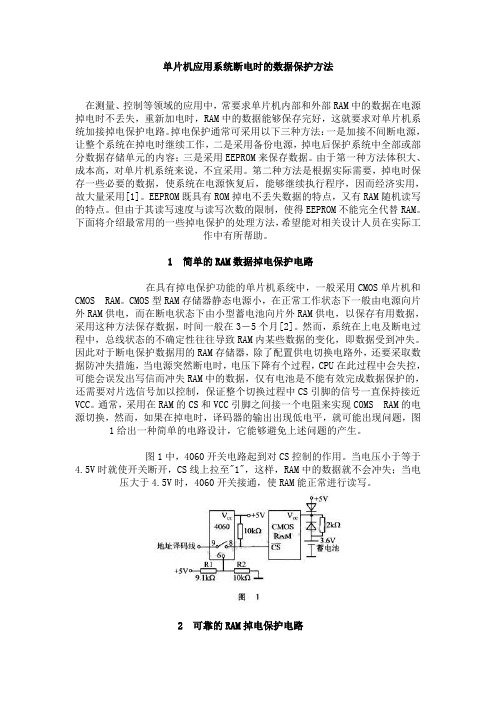
通常,采用在RAM的CS和VCC引脚之间接一个电阻来实现COMS RAM的电源切换,然而,如果在掉电时,译码器的输出出现低电平,就可能出现问题,图1给出一种简单的电路设计,它能够避免上述问题的产生。


常用整流二极管
常用整流二极管分为钼金属势垒二极管、硅势垒二极管和肖特基势垒二极管三种。
一、钼金属势垒二极管(MBD)
这种二极管是由钼及其氧化物层构成,属于高频整流电路中的一种。
其特点是速度快、噪声小、温度系数小、稳定性好,但是抗反向电压、耐过电流、温度特性不够理想。
硅势垒二极管是一种超高速半导体器件,具有非常高的工作频率,常用于频率高、电
压低的电路中。
其特点是速度快、功率损耗小、反向漏电流小、耐受高温、耐久性强,但
是使用环境要求高,抗过电流和反向电压能力略低。
三、肖特基势垒二极管(SJT)
肖特基势垒二极管是一种低功耗、高速度的半导体器件,优于硅势垒二极管和普通整
流二极管。
其特点是速度快、反向电流小、低功耗、符合高速数字电路要求,但是稳定性
较差,因而需要进行电压静参数调节。
常见的整流二极管有1N4001、1N4007、1N4148、1N5817、1N5822等等。
这些二极管均具有不可逆性,即电流只能通过一个方向。
其中1N4001对应的最大反向电压为50V,最大直流工作电流为1A;1N4148对应的最大反向电压为100V,最大工作电流为0.2A。
用户在
选择二极管时,应根据实际情况选用适当的型号,以确保电路正常运行。
常用稳压二极管型号及参数常用的稳压二极管型号有:1N4148、1N4742、1N5231、1N5408、TL431等。
下面将为您逐一介绍它们的参数:1N4148是一种小功率、快速开关二极管。
它的最大可逆工作电压为100V,最大电流为200mA。
该二极管具有快速开关速度和高阻值特性,适用于一些需要高速开关以及低噪声的应用。
1N4742是一种1W的稳压二极管。
它的最大可逆工作电压为12V,最大电流为1W/400mA。
该二极管采用了玻璃封装,适用于一些低功耗稳压应用,例如电源电压调整和参考电压源。
1N5231是一种高精度稳压二极管。
它的最大可逆工作电压为5.1V,最大电流为500mW/165mA。
该二极管可提供精确的稳定电压,适用于一些需要稳定参考电压的应用,例如模拟电路和通信设备。
1N5408是一种高功率整流二极管。
它的最大可逆工作电压为1000V,最大电流为3A。
该二极管具有大功率承受能力和低导通压降特性,适用于需要大电流整流和电源转换的应用,例如电源适配器和开关电源。
TL431是一种调节管(也被称为可编程稳压二极管)。
它的最大可逆工作电压为37V,最大电流为100mA。
该二极管具有精确的稳定电压和调节特性,广泛应用于电源稳压、电流控制和电压参考等场景。
此外,不同厂家还生产并提供其他稳压二极管型号,例如常用的1N5817、1N5819、1N5822、1N5338等。
这些二极管具有不同的最大可逆工作电压和最大电流等参数,可以根据具体应用的需求选择适合的型号。
总之,稳压二极管是一类常见的半导体器件,根据其特性和参数的不同,可以在各种电子设备和电路中实现电压稳定、电流控制等功能。
根据应用需求,可以选择合适的型号和规格的稳压二极管。

Dimensions in millimeters and inchesConform to JEDEC Outline DO-204AL (DO-41)CASE STYLE AND DIMENSIONSMajor Ratings and Characteristics I F(AV)Rectangular1.0Awaveform V RRM20V I FSM @ tp = 5 µs sine 240A V F @1 Apk, TJ = 25°C 0.45V TJrange- 65 to 150°CCharacteristics1N5817UnitsThe 1N5817 axial leaded Schottky rectifier has been optimized for very low forward voltage drop, with moderate leakage.Typical applications are in switching power supplies, convert-ers, free-wheeling diodes, and reverse battery protection.Low profile, axial leaded outlineHigh purity, high temperature epoxy encapsulation for enhanced mechanical strength and moisture resistance Very low forward voltage drop High frequency operationGuard ring for enhanced ruggedness and long term reliabilityDescription/FeaturesSCHOTTKY RECTIFIER1.0 Amp1N5817Bulletin PD-20646 rev. B 05/0211N5817Bulletin PD-20646 rev. B 05/02V FM Max. Forward Voltage Drop(1)0.420.45V @ 1A 0.500.75V @ 3A I RM Max. Reverse Leakage Current (1)0.012 1.0mA T J = 25 °C 2.010mA T J = 100 °C C T Typical Junction Capacitance 110-pF V R = 5V DC (test signal range 100kHz to 1Mhz), @ 25°CL STypical Series Inductance8.0-nH Measured lead to lead 5mm from package body dv/dt Max. Voltage Rate of Change-10000V/ µs(Rated V R )Part number1N5817V RMax. DC Reverse Voltage (V)V RWM Max. Working Peak Reverse Voltage (V)Voltage RatingsI F(AV)Max. Average Forward Current 1.0A 50% duty cycle @ T L = 138 °C, rectangular wave form I FSMMax. Peak One Cycle Non-Repetitive 2405µs Sine or 3µs Rect. pulseSurge Current, @ T J = 25°C4010ms Sine or 6ms Rect. pulse Absolute Maximum RatingsParameters1N5817UnitsConditionsFollowing any rated load condition and withrated V RRM appliedA(1) Pulse Width < 300µs, Duty Cycle <2%20T J = 25 °C Electrical SpecificationsParametersTyp.Max.UnitsConditionsV R = rated V RT J Max. J unction T emperature R ange (2)- 65 to 150°C T stgMax. Storage Temperature Range- 65 to 150°CR thJL Max. Thermal Resistance Junction32°C/W DC operation, Lead lenght = 1/8 inch.to Lead R thJA Max. Thermal Resistance Junction100°C/W DC operation, without cooling finto Ambient WtApproximate Weight 0.33(0.012)gr (oz)Case StyleD O-204AL (DO-41)Parameters1N5817UnitsConditions< thermal runaway condition for a diode on its own heatsink Thermal-Mechanical Specifications(2) dPtot1dTjRth( j-a)1N5817Bulletin PD-20646 rev. B 05/02 Array 31N5817Bulletin PD-20646 rev. B 05/021N5817Bulletin PD-20646 rev. B 05/025 233 Kansas St., El Segundo, California 90245, USA Tel: (310) 252-7105TAC Fax: (310) 252-7309Visit us at for sales contact information. 05/02。
DATA SHEETProduct specificationSupersedes data of April 19921996May 031N5817; 1N5818; 1N5819Schottky barrier diodesfpageM3D119Schottky barrier diodes1N5817; 1N5818; 1N5819FEATURES•Low switching losses•Fast recovery time•Guard ring protected •Hermetically sealed leaded glass package.APPLICATIONS•Low power, switched-mode power supplies•Rectifying•Polarity protection.DESCRIPTIONThe 1N5817 to 1N5819 types are Schottky barrier diodes fabricated in planar technology, and encapsulated in SOD81 hermetically sealed glass packages incorporating Implotec TM(1) technology.(1)Implotec is a trademark of Philips.Fig.1 Simplified outline (SOD81) and symbol.handbook, 4 columnsakMAM218Schottky barrier diodes1N5817; 1N5818; 1N5819LIMITING VALUESIn accordance with the Absolute Maximum Rating System (IEC 134).Notes1.Refer to SOD81 standard mounting conditions.2.For Schottky barrier diodes thermal run-away has to be considered, as in some applications, the reverse powerlosses P R are a significant part of the total power losses. Nomograms for determination of the reverse power losses P R and I F(AV) rating will be available on request.SYMBOL PARAMETERCONDITIONSMIN.MAX.UNITV Rcontinuous reverse voltage1N5817−20V 1N5818−30V 1N5819−40V V RSMnon-repetitive peak reverse voltage 1N5817−24V 1N5818−36V 1N5819−48V V RRMrepetitive peak reverse voltage 1N5817−20V 1N5818−30V 1N5819−40V V RWMcrest working reverse voltage 1N5817−20V 1N5818−30V 1N5819−40V I F(AV)average forward currentT amb =55°C; R th j-a =100K/W;note 1; V R(equiv)=0.2V; note 2−1A I FSMnon-repetitive peak forward currentt =8.3ms half sine wave;JEDEC method;T j =T j max prior to surge:V R =0−25AT stg storage temperature −65+175°C T j junction temperature−125°CSchottky barrier diodes1N5817; 1N5818; 1N5819ELECTRICAL CHARACTERISTICST amb=25°C; unless otherwise specified.SYMBOL PARAMETER CONDITIONS MIN.TYP.MAX.UNIT V F forward voltage see Fig.21N5817I F=0.1A−−320mVI F=1A−−450mVI F=3A−−750mVV F forward voltage see Fig.21N5818I F=0.1A−−330mVI F=1A−−550mVI F=3A−−875mVV F forward voltage see Fig.21N5819I F=0.1A−−340mVI F=1A−−600mVI F=3A−−900mVI R reverse current V R=V RRMmax; note1−−1mAV R=V RRMmax; T j=100°C−−10mAC d diode capacitance V R=4V; f=1MHz1N5817−80−pF1N5818−50−pF1N5819−50−pFNote1.Pulsed test: t p=300µs;δ=0.02.THERMAL CHARACTERISTICSSYMBOL PARAMETER CONDITIONS VALUE UNIT R th j-a thermal resistance from junction to ambient note1100K/W Note1.Refer to SOD81 standard mounting conditions.Schottky barrier diodes1N5817; 1N5818; 1N5819GRAPHICAL DATAhandbook, halfpage0151MBE6342340.5V F (V)I F(A)T j = 125 o C25 o CFig.2 Typical forward voltage.Fig.31N817. Maximum values steady state forward power dissipation as a function of the average forward current; a =I F(RMS)/I F(AV).2100.5 1.5MBE6421(W)0.5P F(AV)I F(AV) (A)a = 32.51.571.4212Schottky barrier diodes 1N5817; 1N5818; 1N5819Fig.41N5818. Maximum values steady state forward power dissipation as a function of the average forward current; a =I F(RMS)/I F(AV).2100.5 1.5MBE6411(W)0.5P F(AV)I F(AV) (A)a = 32.51.571.4212Fig.51N5819. Maximum values steady state forward power dissipation as a function of the average forward current; a =I F(RMS)/I F(AV).2100.5 1.5MBE6431(W)0.5P F(AV)I F(AV) (A)a = 32.51.571.4212Schottky barrier diodes 1N5817; 1N5818; 1N5819Fig.61N5817. Maximum permissible junction temperature as a function of reverse voltage;R th j-a =100K/W.handbook, halfpage020200150500100MBG43410V R (V)T j(oC)V RWM δ = 0.2V RV RWM δ = 0.5Fig.71N5817. Reverse power dissipation as a function of reverse voltage (max. values);R th j-a =100K/W.handbook, halfpage0200.200.150.050.10MBG43510V R (V)P R (W)V RWM δ = 0.2V RV RWM δ = 0.5Fig.81N5818. Maximum permissible junction temperature as a function of reverse voltage;R th j-a =100K/W.handbook, halfpage0102030200150500100MBG432V R (V)T j (o C)V RWM δ = 0.2V RV RWM δ = 0.5Fig.91N5818. Reverse power dissipation as a function of reverse voltage (max. values);R th j-a =100K/W.handbook, halfpage00.200.150.050.10MBG437203010V R (V)P R(W)V RWM δ = 0.2V RV RWM δ = 0.5Schottky barrier diodes 1N5817; 1N5818; 1N5819Fig.101N5819. Maximum permissible junctiontemperature as a function of reverse voltage;R th j-a =100K/W.handbook, halfpage010204020015050100MBG43330V R(V)T j (o C)V RWM δ = 0.2V RV RWM δ = 0.5Fig.111N5819. Reverse power dissipation as afunction of reverse voltage (max. values);R th j-a =100K/W.handbook, halfpage0400.200.150.050.10MBG436203010V R(V)P R(W)V RWM δ = 0.2V RV RWM δ = 0.5Schottky barrier diodes1N5817; 1N5818; 1N5819PACKAGE OUTLINEDEFINITIONS LIFE SUPPORT APPLICATIONSThese products are not designed for use in life support appliances, devices, or systems where malfunction of these products can reasonably be expected to result in personal injury. Philips customers using or selling these products for use in such applications do so at their own risk and agree to fully indemnify Philips for any damages resulting from such improper use or sale.Data sheet status Objective specification This data sheet contains target or goal specifications for product development.Preliminary specification This data sheet contains preliminary data; supplementary data may be published later.Product specification This data sheet contains final product specifications.Limiting valuesLimiting values given are in accordance with the Absolute Maximum Rating System (IEC 134). Stress above one or more of the limiting values may cause permanent damage to the device. These are stress ratings only and operation of the device at these or at any other conditions above those given in the Characteristics sections of the specification is not implied. Exposure to limiting values for extended periods may affect device reliability.Application informationWhere application information is given, it is advisory and does not form part of the specification.Dimensions in mm.Fig.12 SOD81.handbook, full pagewidthMBC0515 max3.8 max 28 min 28 min0.81max2.15max。
1N5817, 1N5818, 1N58191N5817 and 1N5819 are Preferred DevicesAxial Lead Rectifiers...employing the Schottky Barrier principle in a large area metal-to-silicon power diode. State-of-the-art geometry features chrome barrier metal, epitaxial construction with oxide passivation and metal overlap contact. Ideally suited for use as rectifiers in low-voltage, high-frequency inverters, free wheeling diodes, andpolarity protection diodes.•Extremely Low V F•Low Stored Charge, Majority Carrier Conduction•Low Power Loss/High EfficiencyMechanical Characteristics•Case: Epoxy, Molded•Weight: 0.4 gram (approximately)•Finish: All External Surfaces Corrosion Resistant and Terminal Leads are Readily Solderable•Lead and Mounting Surface Temperature for Soldering Purposes: 220°C Max. for 10 Seconds, 1/16″ from case•Shipped in plastic bags, 1000 per bag.•Available Tape and Reeled, 5000 per reel, by adding a “RL” suffix to the part number•Polarity: Cathode Indicated by Polarity Band•Marking: 1N5817, 1N5818, 1N5819MAXIMUM RATINGSPreferred devices are recommended choices for future use and best overall value.MAXIMUM RATINGSTHERMAL CHARACTERISTICS (Note 1)ELECTRICAL CHARACTERISTICS (T = 25°C unless otherwise noted) (Note 1)1.Lead Temperature reference is cathode lead 1/32″ from case.2.Pulse Test: Pulse Width = 300 µs, Duty Cycle = 2.0%.1251151059585752015107.05.04.03.02.0T R , R E F E R E N C E T E M P E R A T U R E (°C )V R , DC REVERSE VOLTAGE (VOLTS)Figure 1. Maximum Reference Temperature1N5817125115105Figure 2. Maximum Reference Temperature1N5818125115105Figure 3. Maximum Reference Temperature1N5819CircuitLoadHalf WaveResistiveCapacitive*Full Wave, Bridge ResistiveCapacitiveFull Wave, Center Tapped*†ResistiveCapacitiveSine WaveSquare Wave0.50.751.31.50.50.750.650.751.01.51.31.5T R , R E F E R E N C E T E M P E R A T U R E (C )°V R , DC REVERSE VOLTAGE (VOLTS)V R , DC REVERSE VOLTAGE (VOLTS)*Note that V R(PK) 9 2.0 V in(PK).†Use line to center tap voltage for V in .Table 1. Values for Factor FT R , R E F E R E N C E T E M P E R A T U R E (°C )NOTE 1. — DETERMINING MAXIMUM RATINGSReverse power dissipation and the possibility of thermal runaway must be considered when operating this rectifier at reverse voltages above 0.1 V RWM . Proper derating may be accomplished by use of equation (1).T A(max) =where T A(max) =T J(max) =P F(AV) =P R(AV) =R θJA =T J(max) - R θJA P F(AV) - R θJA P R(AV)Maximum allowable ambient temperatureMaximum allowable junction temperature(1)Average forward power dissipation (125°C or the temperature at which thermal runaway occurs, whichever is lowest)Average reverse power dissipationJunction-to-ambient thermal resistanceFigures 1, 2, and 3 permit easier use of equation (1) by taking reverse power dissipation and thermal runaway into consideration. The figures solve for a reference temperature as determined by equation (2).T R = T J(max) - R θJA P R(AV)(2)Substituting equation (2) into equation (1) yields:T A(max) = T R - R q JA P F(AV)(3)Inspection of equations (2) and (3) reveals that T R is the ambient temperature at which thermal runaway occurs or where T J = 125°C, when forward power is zero. The transition from one boundary condition to the other is evident on the curves of Figures 1, 2, and 3 as a difference in the rate of change of the slope in the vicinity of 115°C. The data of Figures 1, 2, and 3 is based upon dc conditions. For use in common rectifier circuits, Table 1 indicates suggested factors for an equivalent dc voltage to use for conservative design, that is:(4)V R(equiv) = V in(PK) x FThe factor F is derived by considering the properties of the various rectifier circuits and the reverse characteristics of Schottky diodes.EXAMPLE: Find T A(max) for 1N5818 operated in a 12-volt dc supply using a bridge circuit with capacitive filter such that I DC = 0.4 A (I F(A V) = 0.5 A), I (FM)/I (A V) = 10, Input V oltage = 10 V (rms), R θJA = 80°C/W.Step 1. Find V R(equiv). Read F = 0.65 from Table 1,∴ V R(equiv) = (1.41)(10)(0.65) = 9.2 V.Step 2. Find T R from Figure 2. Read T R = 109°C @ V R = 9.2 V and R θJA = 80°C/W.Step 3. Find P F(AV) from Figure 4. **Read P F(AV) = 0.5 W@I (FM)I (AV)= 10 and IF(AV) = 0.5 A.Step 4. Find T A(max) from equation (3).T A(max) = 109 - (80) (0.5) = 69°C.**Values given are for the 1N5818. Power is slightly lower for the 1N5817 because of its lower forward voltage, and higher for the 1N5819.7/82040509080706030103/45/81/23/81/41.01/81R θJ L , T H E R M A L R E S I S T A N C E , J U N C T I O N −T O −L E A D (°C /W )L, LEAD LENGTH (INCHES)Figure 4. Steady-State Thermal Resistance0.070.054.02.01.00.80.60.40.2P F (A V ), A V E R A G E P O W E R D I S S I P A T I O N (W A T T S )I F(AV), AVERAGE FORWARD CURRENT (AMP)r (t ), T R A N S I E N T T H E R M A L R E S I S T A N C E (N O R M A L I Z E D )t, TIME (ms)NOTE 2. — MOUNTING DATAData shown for thermal resistance junction-to-ambient (R θJA ) for the mountings shown is to be used as typical guide-line values for preliminary engineering, or in case the tie point temperature cannot be measured.TYPICAL VALUES FOR R θJA IN STILL AIRMounting Method1/81/41/23/4Lead Length, L (in)R θJA 12352676580728785100°C/W °C/W °C/W50Mounting Method 1P .C. Board with 1-1/2″ x 1-1/2″copper surface.Mounting Method 3P .C. Board with 1-1/2″ x 1-1/2″copper surface.VECTOR PIN MOUNTINGFigure 5. Forward Power Dissipation1N5817-19Figure 6. Thermal Response125115105958575155.03.02.00.30.20.140361230201.00.50.050.032416208.04.028032NOTE 3. — THERMAL CIRCUIT MODEL(For heat conduction through the leads)v F, INSTANTANEOUS FORWARD VOLTAGE (VOLTS)iF,INSTANTANEOUSFORWARDCURRENT(AMP)Figure 7. Typical Forward VoltageIFSM,PEAKSURGECURRENT(AMP)NUMBER OF CYCLESFigure 8. Maximum Non-Repetitive Surge CurrentIR,REVERSECURRENT(mA)V R, REVERSE VOLTAGE (VOLTS)Figure 9. Typical Reverse Current Use of the above model permits junction to lead thermal re-sistance for any mounting configuration to be found. For agiven total lead length, lowest values occur when one side ofthe rectifier is brought as close as possible to the heatsink.Terms in the model signify:T A = Ambient Temperature T C = Case TemperatureT L = Lead Temperature T J = Junction TemperatureRθS = Thermal Resistance, Heatsink to AmbientRθL = Thermal Resistance, Lead to HeatsinkRθJ = Thermal Resistance, Junction to CaseP D = Power Dissipation(Subscripts A and K refer to anode and cathode sides, re-spectively.) Values for thermal resistance components are:RθL = 100°C/W/in typically and 120°C/W/in maximumRθJ = 36°C/W typically and 46°C/W maximum.NOTE 4. — HIGH FREQUENCY OPERATIONSince current flow in a Schottky rectifier is the result of majority carrier conduction, it is not subject to junction diode forward and reverse recovery transients due to minor-ity carrier injection and stored charge. Satisfactory circuit analysis work may be performed by using a model consist-ing of an ideal diode in parallel with a variable capacitance. (See Figure 10.)Rectification efficiency measurements show that opera-tion will be satisfactory up to several megahertz. For exam-ple, relative waveform rectification efficiency is approxi-mately 70 percent at 2.0 MHz, e.g., the ratio of dc power to RMS power in the load is 0.28 at this frequency, whereasperfect rectification would yield 0.406 for sine wave inputs. However, in contrast to ordinary junction diodes, the loss in waveform efficiency is not indicative of power loss: it is simply a result of reverse current flow through the diode ca-pacitance, which lowers the dc output voltage.10200.870200100503020106.04.02.01.00.68.00.440 C,CAPACITANCE(pF)V R, REVERSE VOLTAGE (VOLTS)Figure 10. Typical CapacitancePACKAGE DIMENSIONSCASE 59-10ISSUE SAXIAL LEAD, DO-41DIM MIN MAX MIN MAX MILLIMETERSINCHES A 4.10 5.200.1610.205B 2.00 2.700.0790.106D 0.710.860.0280.034F −−− 1.27−−−0.050K25.40−−−1.000−−−NOTES:1.DIMENSIONING AND TOLERANCING PER ANSI Y14.5M, 1982.2.CONTROLLING DIMENSION: INCH.3.59−04 OBSOLETE, NEW STANDARD 59−09.4.59−03 OBSOLETE, NEW STANDARD 59−10.5.ALL RULES AND NOTES ASSOCIATED WITH JEDEC DO−41 OUTLINE SHALL APPLY6.POLARITY DENOTED BY CATHODE BAND.7.LEAD DIAMETER NOT CONTROLLED WITHIN F DIMENSION.ON Semiconductor and are registered trademarks of Semiconductor Components Industries, LLC (SCILLC). SCILLC reserves the right to make changes without further notice to any products herein. SCILLC makes no warranty, representation or guarantee regarding the suitability of its products for any particular purpose, nor does SCILLC assume any liability arising out of the application or use of any product or circuit, and specifically disclaims any and all liability, including without limitation special, consequential or incidental damages. “Typical” parameters which may be provided in SCILLC data sheets and/or specifications can and do vary in different applications and actual performance may vary over time. All operating parameters, including “Typicals” must be validated for each customer application by customer’s technical experts. SCILLC does not convey any license under its patent rights nor the rights of others.SCILLC products are not designed, intended, or authorized for use as components in systems intended for surgical implant into the body, or other applications intended to support or sustain life, or for any other application in which the failure of the SCILLC product could create a situation where personal injury or death may occur. Should Buyer purchase or use SCILLC products for any such unintended or unauthorized application, Buyer shall indemnify and hold SCILLC and its officers, employees, subsidiaries, affiliates, and distributors harmless against all claims, costs, damages, and expenses, and reasonable attorney fees arising out of, directly or indirectly, any claim of personal injury or death associated with such unintended or unauthorized use, even if such claim alleges that SCILLC was negligent regarding the design or manufacture of the part. SCILLC is an Equal Opportunity/Affirmative Action Employer. PUBLICATION ORDERING INFORMATIONJAPAN: ON Semiconductor, Japan Customer Focus Center2-9-1 Kamimeguro, Meguro-ku, Tokyo, Japan 153-0051Phone: 81-3-5773-3850。
肖特基二极管、型号的命名、字母含义、解释肖特基二极管的命名:肖特基二极管是以其发明人肖特基博士(Schottky)命名的,完整的叫法是:肖特基整流二极管(Schottky Rectifier Diode 缩写成 SR),也有人叫做:肖特基势垒二极管(Schottky Barrier Diode 缩写成 SBD)的简称。
肖特基:Schottky整流:RectifierSR:即为肖特基整流二极管Schottky Rectifier Diode:肖特基整二极管,简称:SR,比如:SR107,SR10100CT......肖特基:Schottky势垒:BarrierSB:即为肖特基势垒二极管肖特基二极管也称肖特基势垒二极管(简称SBD),国内厂家也有叫做“SB1045CT、SR10100、SL....、BL....Schottky Barrier Diode:肖特基势垒二极管,简称:SB,比如:SB107,SB1045CT......Schottky Barrier Diode:也有简写为:SBD 来命名产品型号前缀的。
但 SBD 不是利用 P 型半导体与 N 型半导体接触形成PN 结原理制作的,而是利用金属与半导体接触形成的金属-半导体结原理制作的。
因此,SBD 也称为金属-半导体(接触)二极管或表面势垒二极管,它是一种热载流子二极管。
关于肖特基 MBR 系列为什么国际通用常见的肖特基二极管都以“MBR”字头命名?因为最早是世界著名半导体公司-摩托罗拉半导体命名的产品型号M:是以最早 MOTOROLA 的命名,取 MB:Bridge 桥;Barrier:势垒R:Rectifier,整流器“MBR”意为整流器件SCHOTTKY:肖特基 SCHOTTKY RECTIFIER DIODES:肖特基整流二极管。
例如:MBR10200CT M:MOTOROLA 缩写 MB:Barrier1 缩写 BR:Rectifier 缩写 R10:电流 10A200:电压 200VC:表示 TO-220AB 封装,常指半塑封。