ADI University Program - MEMS Workshop
- 格式:pdf
- 大小:5.82 MB
- 文档页数:87

执教全美Top 50大学的中科大毕业生======麻省理工学院(私立)3人文晓刚,麻省理工学院物理系,Full Professor,物理系82届(772),1981年CUSPEA全国状元/physics/facultyandstaff/faculty/xiaogang_wen.html/~wen/刘洪,麻省理工学院物理系,Assistant Prof,近代物理系93届(894)/physics/facultyandstaff/faculty/hong_liu.html林间,WHOI-MIT Joint Program教授,WHOI Associate Scientist with Tenure,地球与空间科学系(777)/dept/profile.go?id=294/oceanus/viewArticle.do?id=4009======斯坦福大学(私立)5人王善祥,斯坦福大学电子工程系与材料科学系,Full Professor,物理系86届(812)/research/layout.php?sunetid=sxwan骆利群,斯坦福大学神经生物学系,Full Professor,少年班86届(81少)/profiles/Liqun_Luo/范汕洄,斯坦福大学电子工程系,Assistant Prof,00班92届物理(8800)/~shanhui崔屹,斯坦福大学材料科学与工程系,Assistant Prof,化学系98届(9312)/about_faculty/mse_fac_profile2.php?sunetid=yicui崔便晓,斯坦福大学化学系,Assistant Prof,高分子系98届(9314)/dept/chemistry/department/news/archives/2007/04/new_faculty_mem_1.html======加州大学柏克利分校(公立)7+加州大学旧金山分校(公立)2人(注:后者常被认为是前者的医学院)刘奋勇,加州大学柏克利分校公共卫生学院,Full Professor,生物系86届(818)/~microbes/faculty/liu.html周强,加州大学柏克利分校分子与细胞生物学系,Associate Professor,生物系86届(818)/faculty/BMB/zhouq.html肖强,加州大学伯克利分校新闻学院,Lecturer(该院教师都是Lecturer),地球物理86届(817)/program/newmedia/faculty/罗坤忻(女),加州大学柏克利分校分子与细胞生物学系,Associate Professor,生物系86届(828)/faculty/CDB/luok.html郭新(女),加州大学伯克利分校工业工程与运筹学系,Assistant Prof,数学系92届(871)/People/Faculty/xinguo.htm杨培东,加州大学柏克利分校化学系,Associate Professor,应用化学系93届(8812)/faculty/Yang/Peidong-Yang.html陈路(女),加州大学伯克利分校分子与细胞生物学系,Assistant Professor,生物系93届(898),美国麦克阿瑟基金会“天才奖”得主/faculty/NEU/chenl.html汤超,加州大学旧金山分校生物医药系,Full Professor,力学与机械工程系82届(775)/dbps/faculty/pages/tang.html刘立民,加州大学旧金山分校癌症中心,Assistant Professor,生物系86届(818)/people/liu_limin.php======哈佛大学(私立)7人王家槐,哈佛大学医学院,Associate Prof,63届/WhitePagesPublic.asp?task=showperson&id=177271374174279373178273&a=hms&r=96&kw=wang,,,/Collaborators/Wang.html黄旭东,哈佛大学医学院,Assistant Prof,化学87届(823&8212)/staff/xudongHuang.htm/cagn/Faculty/huang.html王瑛(女),哈佛大学医学院,Assistant Prof,应用化学91届(8612)/wang_y.htm/people.php?people_id=767庄小威(女),哈佛大学物理系和化学系,Full Professor,少年班91届物理专业(87 少),女,少年班,美国麦克阿瑟基金会“天才奖”得主,美国Searle学者奖得主。
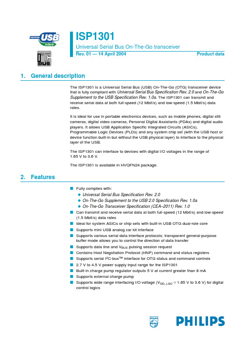
ISP1301Universal Serial Bus On-The-Go transceiverRev. 01 — 14 April 2004Product data1.General descriptionThe ISP1301 is a Universal Serial Bus (USB) On-The-Go (OTG) transceiver devicethat is fully compliant with Universal Serial Bus Specification Rev.2.0and On-The-GoSupplement to the USB Specification Rev.1.0a. The ISP1301 can transmit andreceive serial data at both full-speed (12Mbit/s) and low-speed (1.5Mbit/s) datarates.It is ideal for use in portable electronics devices, such as mobile phones, digital stillcameras, digital video cameras, Personal Digital Assistants (PDAs) and digital audioplayers. It allows USB Application Specific Integrated Circuits (ASICs),Programmable Logic Devices (PLDs) and any system chip set (with the USB host ordevice function built-in but without the USB physical layer)to interface to the physicallayer of the USB.The ISP1301 can interface to devices with digital I/O voltages in the range of1.65V to3.6V.The ISP1301 is available in HVQFN24 package.2.Featuress Fully complies with:x Universal Serial Bus Specification Rev.2.0x On-The-Go Supplement to the USB2.0 Specification Rev.1.0ax On-The-Go Transceiver Specification (CEA–2011) Rev.1.0s Can transmit and receive serial data at both full-speed (12Mbit/s) and low-speed(1.5Mbit/s) data ratess Ideal for system ASICs or chip sets with built-in USB OTG dual-role cores Supports mini USB analog car kit interfaces Supports various serial data interface protocols; transparent general-purposebuffer mode allows you to control the direction of data transfers Supports data line and V BUS pulsing session requests Contains Host Negotiation Protocol (HNP) command and status registerss Supports serial I2C-bus™ interface for OTG status and command controlss 2.7V to4.5V power supply input range for the ISP1301s Built-in charge pump regulator outputs 5V at current greater than 8mAs Supports external charge pumps Supports wide range interfacing I/O voltage(V DD_LGC=1.65V to3.6V)for digitalcontrol logicss8kV built-in electrostatic discharge(ESD)protection on the DP,DM,V BUS and IDliness Full industrial grade operation from−40°C to+85°Cs Available in a small HVQFN24 (4×4mm2) halogen-free and lead-free package.3.Applicationss Mobile phones Digital cameras Personal digital assistants Digital video recorder.4.AbbreviationsASIC —Application-Specific Integrated CircuitATX —Analog USB transceiverHNP —Host Negotiation ProtocolESD —ElectroStatic DischargeI2C-bus —Inter IC-busIC —Integrated CircuitOTG —On-The-GoPDA —Personal Digital AssistantSE0 —Single-Ended zeroSOF —Start-of-FrameSRP —Session Request ProtocolUSB —Universal Serial BusUSB-IF —USB Implementers Forum.5.Ordering informationTable 1:Ordering informationType number PackageName Description VersionISP1301BS HVQFN24plastic thermal enhanced very thin quadflat package;no leads; 24terminals; body 4×4×0.85mmSOT616-16.Block diagramFig 1.Block diagram.3.3 V DC-DC REGULATORV REG(3V3)004aaa195LEVEL SHIFTERSERIAL CONTROLLERUSBTRANSCEIVERCOMPARATORSID DETECTORPULL-UP AND PULL-DOWN RESISTORSV BUS CHARGE PUMPV BUS RESET_NSUSPENDSPEED VM VP RCV SE0/VMDAT/VP OE_N/INT_N91413121110684INT_NADR/PSWSDA SCL 321517DGND AGNDV DD_LGCV BAT2221C2C1V BUS19CGND 23ID18DM 15DP1672024exposed die padCARKIT INTERRUPT DETECTORISP13017.Pinning information7.1PinningFig 2.Pin configuration HVQFN24 (top view).Fig 3.Pin configuration HVQFN24 (bottom view).879101112232422212019321654161718131415ISP1301BSSPEEDINT_N RESET_NSCL SDA ADR/PSWV D D _L G CC G N DC 2C 1V B A T V B U S SE0/VMDAT/VP DM DP AGND ID V R E G (3V 3)O E _N /I N T _NV MV PR C VS U S P E N D004aaa542terminal 1232422212019879101112456123151413181716ISP1301BSADR/PSWSDA SCL RESET_NINT_N SPEED V R E G (3V 3)S U S P E N DO E _N /I N T _NV MV PR C VIDAGND DP DM DAT/VP SE0/VM V D D _L G CC 2C 1V B A TV B U SC G N DDGND(exposed die pad)004aaa196Bottom view7.2Pin descriptionTable 2:Pin description[1]Symbol[2]Pin Type[3]ResetvalueDescriptionADR/PSW1I/O high-Z ADR input —sets the least-significant I2C-busaddress bit of the ISP1301; latched-on reset(including power-on reset)PSW output —enables or disables the externalcharge pump after resetbidirectional; push-pull input; three-state output SDA2I/OD high-Z serial I2C-bus data input and outputbidirectional; push-pull input; open-drain output SCL3I/OD high-Z serial I2C-bus clock input and outputbidirectional; push-pull input; open-drain output RESET_N4I-asynchronous reset; active LOWpush-pull inputINT_N5OD high-Z interrupt output; active LOWopen-drain outputSPEED6I-speed selection input for the ATX;effective whenbit SPD_SUSP_CTRL=0:•LOW: low-speed•HIGH: full-speed.push-pull inputV REG(3V3)7P-output of the internal voltage regulator; anexternal decoupling capacitor of 0.1µF isrequiredSUSPEND8I-suspend selection input for A TX; effective whenbit SPD_SUSP_CTRL=0:•LOW: normal operating•HIGH: suspend.push-pull inputOE_N/ INT_N 9I/O high-Z OE_N input —enable driving DP and DM whenin the USB modeINT_N output —interrupt (push pull) whensuspended and bit OE_INT_EN=1bidirectional; push-pull input; three-state outputVM10O-single-ended DM receiver outputpush-pull outputVP11O-single-ended DP receiver outputpush-pull outputRCV12O0differential receiver output; reflects thedifferential value of DP and DMpush-pull output[1] A detailed description of these pins can be found in Section 8.9.[2]Symbol names ending with underscore N (for example, NAME_N) indicate active LOW signals.[3]I =input; O =output; I/O =digital input/output; OD =open-drain output; AI/O =analog input/output;P =power or ground pin.[4]High-Z when pin OE_N/INT_N is LOW. Driven LOW when pin OE_N/INT_N is HIGH.SE0/VM13I/O-[4]SE0 (input and output) —SE0 function in DA T_SE0 USB modeVM (input and output) —VM function in VP_VM USB modebidirectional; push-pull input; three-state outputDA T/VP 14I/O -[4]DAT (input and output) —DAT function in DA T_SE0 USB modeVP (input and output) —VP function in VP_VM USB modebidirectional; push-pull input; three-state outputDM 15AI/O -USB data minus pin (D −)DP 16AI/O -USB data plus pin (D+)AGND 17P -analog groundID18AI/O-identification detector input and output;connected to the ID pin of the USB mini receptacleV BUS19AI/O -V BUS line input and output of the USB interface;place an external decoupling capacitor of 0.1µF close to this pinV BAT 20P -supply voltage (2.7V to 4.5V)C121AI/O -charge pump capacitor pin 1; typically use a 100nF capacitor between pins C1 and C2C222AI/O -charge pump capacitor pin 2; typically use a 100nF capacitor between pins C1 and C2CGND 23P -ground for the charge pumpV DD_LGC 24P-supply voltage for the interface logic signals (1.65V to 3.6V)DGNDexposed die padP -digital groundTable 2:Pin description [1]…continued Symbol [2]Pin Type [3]Reset value Description8.Functional description8.1Serial controllerThe serial controller includes the following functions:•I2C-bus slave interface•Interrupt generator•Mode Control registers•OTG registers•Interrupt related registers•Device identification registers.The serial controller acts as an I2C-bus slave, and uses the SCL and SDA pins tocommunicate with the OTG controller.For more details on serial controller, see Section11.8.2V BUS charge pumpThe charge pump supplies current to the V BUS line. It can operate in any of thefollowing modes:•Output 5V at current greater than 8mA•Pull-up V BUS to 3.3V through a resistor (R VBUS(PU)) for initiating V BUS pulsing SRP•Pull-down V BUS to ground through a resistor (R VBUS(PD)) for discharging V BUSbefore initiating SRP.8.3V BUS comparatorsV BUS comparators provide indications regarding the voltage level on V BUS.8.3.1V BUS valid comparatorThis comparator is used by an A-device to determine whether or not the voltage onV BUS is at a valid level for operation. The minimum threshold for the V BUS validcomparator is 4.4V. Any voltage on V BUS below this threshold is considered to be afault. During power up, it is expected that the comparator output will be ignored.8.3.2Session valid comparatorThe session valid comparator is a TTL-level input that determines when V BUS is highenough for a session to start.Both the A-device and the B-device use this comparatorto detect when a session is being started.The A-device also uses this comparator toindicate when a session is completed. The session valid threshold of the ISP1301 isbetween 0.8V and2.0V.8.3.3Session end comparatorThe session end comparator determines when V BUS is below the B-device sessionend threshold of 0.2V to0.8V.8.4ID detectorIn either the active or suspended power mode,the ID detector senses the condition of the ID line and differentiates between the following three conditions:•Pin ID is floating; bit ID_FLOAT=1•Pin ID is shorted to ground; bit ID_GND=1•Pin ID is connected to ground through resistor R ACC_ID; bit ID_FLOA T=0 and bitID_GND=0.The ID detector also has a switch that can be used to ground pin ID. This switch is controlled by bit ID_PULLDOWN in the serial controller.8.5Pull-up and pull-down resistorsThe pull-up and pull-down resistors include the following switchable resistors:•Pin DP pull-up•Pin DP pull-down•Pin DM pull-up•Pin DM pull-down.The pull-up resistor is a context variable as described in the ECN_27%_Resistordocument. The variable pull-up resistor hardware is implemented to meet the USB ECN_27% specification.8.6USB transceiver (ATX)The behavior of the USB transceiver depends on the operation mode of the ISP1301:•In the USB mode, the USB transceiver block performs USB full-speed orlow-speed transceiver functions. This includes differential driver, differentialreceiver and single-ended receivers.•In the transparent general purpose buffer mode or the UART mode, the USBtransceiver block functions as a level shifter between the pins DAT/VP and SE0/VMand the pins DP and DM.8.7 3.3V DC-DC regulatorThe built-in3.3V DC-DC regulator conditions the supply voltage(V BA T)for use in the ISP1301:•V BA T=3.6V to 4.5V: the regulator will output 3.3V±10%•V BA T<3.6V: the regulator will be bypassed.The output of the regulator can be monitored on the V REG(3V3) pin.8.8Car kit interrupt detectorThe car kit interrupt detector is a comparator that detects when the DP line is below the car kit interrupt threshold V PH_CR_INT (0.4V to0.6V). The car kit interruptdetector is enabled in the audio mode only (bit AUDIO_EN=1).8.9Detailed description of pins8.9.1ADR/PSWThe ADR/PSW pin has two functions. On reset (including power-on reset), the level on this pin is latched as ADR_REG,which represents the least significant bit (LSB)of the I 2C address of the ISP1301. If bit ADR_REG =0, the I 2C-bus address for the ISP1301 is 0101100 (0x2C); if bit ADR_REG =1, the I 2C-bus address for the ISP1301 is 0101101 (0x2D).After reset, the ADR/PSW pin can be programmed as an output. If in the Mode Control 2 register bit PSW_OE =1, then the ADR/PSW output will be enabled. The logic level will be determined by bit ADR_REG. If bit ADR_REG =0, then theADR/PSW pin will drive HIGH.If bit ADR_REG =1,then the ADR/PSW pin will drive LOW.The ADR/PSW pin can be used to turn on or off the external charge pump. TheISP1301built-in charge pump supports V BUS current at 8mA.If the application needs more current support (for example, 50mA), an external charge pump may beneeded. In this case, the ADR/PSW pin can act as a power switch for the external charge pump.Figure 4 shows an example of using external charge pump.8.9.2SCL and SDAThe SCL (serial clock) and SDA (serial data) signals implement a two-wire serial I 2C-bus.8.9.3RESET_NActive LOW asynchronous reset for all digital logic.Either connect this pin to V DD_LGC for power-on reset or apply a minimum of 10µs LOW pulse for hardware reset.8.9.4INT_NThe INT_N (interrupt) pin is asserted while an interrupt condition exists. It isdeasserted when the Interrupt Latch register is cleared.The INT_N pin is open-drain,and, therefore, can be connected using a wired-AND with other interrupt signals.Fig ing external charge pump.004aaa437CHARGE PUMPADR/PSWV BUS+3.3 V100 k Ω4.7 µFV BUS ID DM DPGNDV OUTV IN ON/OFFV BATISP13018.9.5OE_N/INT_NPin OE_N/INT_N is normally an input to the ISP1301.When bit TRANSP_EN=0 and bit UART_EN=0, the OE_N/INT_N pin controls the direction of DAT/VP, SE0/VM, DP and DM as indicated in Table4.When suspended (either pin SUSPEND=HIGH or bit SUSPEND_REG=1) and bit OE_INT_EN=1, pin OE_N/INT_N becomes a push-pull output (active LOW) toindicate the interrupt condition.8.9.6SE0/VM, DAT/VP, RCV, VM and VPThe ISP1301 transmits USB data on the USB line under the following conditions:•Bit TRANSP_EN=0•Bit UART_EN=0•Pin OE_N/INT_N=LOW.T able10 shows the operation of the SE0/VM and DAT/VP pins during the transmitoperation. The RCV pin is not used during transmit.The ISP1301 receives USB data from the USB line under the following conditions:•Bit TRANSP_EN=0•Bit UART_EN=0•Pin OE_N/INT_N=HIGH.T able12 shows the operation of the SE0/VM, DA T/VP and RCV pins during thereceive operation.The VP and VM pins are single-ended receiver outputs of the DP and DM pins,respectively.8.9.7DP and DMThe DP(data plus)and DM(data minus)pins implement the USB data signals.When in the transparent general-purpose buffer mode, the ISP1301 operates as a levelshifter between the (DAT/VP, SE0/VM) and (DP, DM) pins.8.9.8IDThe ID (identification) pin is connected to the ID pin on the USB mini receptacle. An internal pull-up resistor (to V REG(3V3)) is connected to this pin. When bitID_PULLDOWN is set, the ID pin will be shorted to ground.8.9.9V BUSThis pin acts as an input to the V BUS comparator or an output from the charge pump.When the VBUS_DRV bit of the OTG Control register is asserted, the ISP1301 tries to drive V BUS to a voltage of 4.4V to5.25V with an output current capability of atleast 8mA.8.9.10V BATThis pin is an input and supplies power to the ISP1301.The ISP1301operates when V BA T is between 2.7V and 4.5V .8.9.11C1 and C2The C1 and C2 pins are for connecting the flying capacitor of the charge pump. The output current capacity of the charge pump depends on the value of the capacitor.For maximum efficiency, place capacitors as close as possible to the pins.[1]For output voltage V BUS > 4.7V (bit VBUS_VLD =1).[2]For V BA T =3.0V to 4.5V .8.9.12V DD_LGCThis pin is an input and sets logic thresholds.It also powers the pads of the following logic pins:•ADR/PSW•DAT/VP , SE0/VM and RCV •VM and VP •INT_N •OE_N/INT_N •RESET_N •SPEED •SUSPEND •SCL and SDA.8.9.13AGND, CGND and DGNDAGND, CGND and DGND are ground pins for analog, charge pump and digitalcircuits,respectively.These pins can be connected separately or together depending on the system performance requirements.Fig 5.Charge pump capacitor.Table 3:Recommended charge pump capacitor valueC ext I L (max)[1]47nF 8mA 100nF18mA [2]004aaa278I L ISP1301V BUSC1C2C ext9.Modes of operationThere are four types of modes in the ISP1301:•Power modes•Direct I2C-bus mode•USB modes•Transparent modes.9.1Power modesThe power modes of the ISP1301 are as follows:•Active power mode: power is on.•USB suspend mode:to reduce power consumption,the USB differential receiver ispowered down.•Global power-down mode: set bit GLOBAL_PWR_DN=1 of the Mode Control2register; the differential transmitter and receiver, clock generator, charge pump,and all biasing circuits are turned off to reduce power consumption to the minimumpossible; for details on waking up the clock, see Section12.9.2Direct I2C-bus modeIn the direct I2C-bus mode, an external I2C-bus master (OTG controller) directlycommunicates with the serial controller through the SCL and SDA lines. The serialcontroller has a built-in I2C-bus slave function.In this mode, an external I2C-bus master can access the internal registers of thedevice (Status, Control, Interrupt, and so on) through the I2C-bus interface.The supported I2C-bus bit rate is 100kbit/s (maximum).The ISP1301is in the direct I2C-bus mode when either bit TRANSP_EN bit=0or pinOE_N/INT_N is deasserted.9.3USB modesThe four USB modes of the ISP1301 are:•VP_VM unidirectional mode•VP_VM bidirectional mode•DAT_SE0 unidirectional mode•DAT_SE0 bidirectional mode.In the VP_VM USB mode, the DAT/VP pin is used for the VP function, the SE0/VMpin is used for the VM function, and the RCV pin is used for the RCV function.In the DA T_SE0USB mode,the DAT/VP pin is used for the DAT function,the SE0/VMpin is used for the SE0 function, and the RCV pin is not used.In the unidirectional mode, the DAT/VP and SE0/VM pins are always inputs. In thebidirectional mode, the direction of these signals depends on the OE_N/INT_N input.T able 6 specifies the functionality of the device during the four USB modes.The ISP1301 is in the USB mode when both the TRANSP_EN and UART_EN bits are cleared.9.4Transparent modes9.4.1Transparent general-purpose buffer modeIn the transparent general-purpose buffer mode, the DA T/VP and SE0/VM pins are connected to the DP and DM pins, respectively. Using bits TRANSP_BDIR1 and TRANSP_BDIR0 of the Mode Control 2 register as specified in Table 8, you can control the direction of data transfer. The ISP1301 is in the transparent general-purpose buffer mode if bit TRANSP_EN =1 and bit DAT_SE0=1.9.4.2Transparent UART modeWhen in the transparent UART mode, the ATX behaves as two logic level translator between the following pins:•For TxD signal: from SE0/VM (V DD_LGC level) to DM (+3.3V level)•For RxD signal: from DP (+3.3V level) to DAT/VP (V DD_LGC level).In the UART mode, the OTG controller is allowed to connect a UART to the DA T/VP and SE0/VM pins of the ISP1301.The UART mode is entered by setting the UART_EN bit in the Mode Control 1register. The UART mode is equivalent to one of the transparent general purpose buffer mode (bit TRANSP_BDIR1=1, bit TRANSP_BDIR0=0).9.4.3Summary tables[1]Conditions:a)bit SPD_SUSP_CTRL =0 and pin SUSPEND =HIGH, or b)bit SPD_SUSP_CTRL =1 and bit SUSPEND_REG =0.Table 4: Device operating modesModeUSB suspend condition [1]Bit DAT_SE0PinOE_N/INT_N Bit TRANSP _EN Bit UART _ EN DescriptionDirect I 2C-bus mode Direct I 2C-bus modeX X X 0X X X HIGH 1X X1X 1X USB modes USB suspend mode 1X X 00see T able 5 and T able 7USB functional mode 0X X 00ATX is fully functional; see T able 6Transparent modes T ransparent general-purpose buffer modeX 1X 10ATX is not functional; see T able 8T ransparent UART modeX XXX1DA T/VP <=DP (RxD signal of UART)SE0/VM =>DM (TxD signal of UART);ATX is not functional[1]In the USB suspend mode, the ISP1301 can drive the DP and DM lines, if the OE_N/INT_N input (when the OE_INT_EN bit is not set) is LOW. In such a case, these outputs are driven as in the USB functional modes,but with the full-speed characteristics,irrespective of the value of the SPEED input pin or the SPEED_REG bit.[1]Some of the modes and signals are provided to achieve backward compatibility with IP cores.[2]TxD+ and TxD − are single-ended inputs for driving the DP and DM outputs, respectively, in the single-ended mode.[3]RxD+ and RxD − are the outputs of the single-ended receivers connected to DP and DM, respectively.[4]TxD is the input for driving DP and DM in the DA T_SE0 mode.[5]FSE0 is for forcing an SE0 on the DP and DM lines in the DA T_SE0 mode.[6]RxD is the output of the differential receiver.[7]RSE0 is an output indicating that an SE0 has been received on the DP and DM lines.Table 5:USB suspend mode: I/OPinFunctionDP as output can be driven if pin OE_N/INT_N is active LOW, otherwise high-Z [1]DM as output can be driven if pin OE_N/INT_N is active LOW, otherwise high-Z [1]V BUS can be driven depending on bit VBUS_DRV SCL connected to SCL I/O of the I 2C-bus slave SDAconnected to SDA I/O of the I 2C-bus slaveTable 6:USB functional modes: I/O values [1]USB modeBit Pin DAT_SE0BI_DI OE_N/INT_N DAT/VP SE0/VM VP VM RCV VP_VM unidirectional 00X TxD+[2]TxD −[2]RxD+[3]RxD −[3]RxD [3]bidirectional01LOW TxD+[2]TxD −[2]01HIGH RxD+[3]RxD −[3]DA T_SE0unidirectional 10X TxD [4]FSE0[5]bidirectional11LOW TxD [4]FSE0[5]11HIGHRxD [6]RSE0[7]Table 7:USB suspend mode: I/O valuesUSB suspend mode Input pin Output pin DPDM DAT/VP SE0/VM VP VM RCV DA T_SE0(bit DA T_SE0=1)LOW LOW LOW HIGH LOW LOW LOW HIGH LOW HIGH LOW HIGH LOW LOW LOW HIGH LOW LOW LOW HIGH LOW HIGHHIGH HIGH LOW HIGH HIGH LOW VP_VM(bit DA T_SE0=0)LOW LOW LOW LOW LOW LOW LOW HIGH LOW HIGH LOW HIGH LOW LOW LOW HIGH LOW HIGH LOW HIGH LOW HIGHHIGHHIGHHIGHHIGHHIGHLOWB transceiver10.1Differential driverThe operation of the driver is described in Table 9.The register bits and the pins used in the column heading are described in Section 11.1 and Section 8.9, respectively.[1]Can be controlled by using either the SUSPEND pin or the SUSPEND_REG bit.10.2Differential receiverT able 11 describes the operation of the differential receiver. The register bits and the pins used in the column heading are described in Section 11.1 and Section 8.9,respectively.Table 8:Transparent general-purpose buffer modeBit TRANSP_BDIR[1:0]Direction of the data flow 00DA T/VP =>DP SE0/VM =>DM 01DA T/VP =>DP SE0/VM <=DM 10DA T/VP <=DP SE0/VM =>DM 11DA T/VP <=DPSE0/VM <=DMTable 9:Transceiver driver operation setting Suspend [1]Bit TRANSP_EN Pin OE_N/INT_N BitDAT_SE0Differential driver00LOW 0output value from DA T/VP to DP and SE0/VM to DMLOW1output value from DAT/VP to DP and DM if SE0/VM is 0; otherwise, drive both DP and DM LOW10LOW X output value from DA T/VP to DP and DM X X HIGH X high-Z X1XXhigh-ZTable 10:USB functional mode: transmit operationUSB mode Input pin Output pin DAT/VP SE0/VM DP DM DA T_SE0LOW LOW LOW HIGH HIGH LOW HIGH LOW LOW HIGH LOW LOW HIGHHIGH LOW LOW VP_VM LOW LOW LOW LOW HIGH LOW HIGH LOW LOW HIGH LOW HIGH HIGHHIGHHIGHHIGHThe detailed behavior of the receive transceiver operation is given in Table 12.[1]Can be controlled by using either the SUSPEND pin or the SUSPEND_REG bit.[1]Can be controlled by using either the SUSPEND pin or the SUSPEND_REG bit.Table 11:Differential receiver operation settings Suspend [1]BitTRANSP_EN PinOE_N/INT_N BitDAT_SE0Differential receiver 1X X X 0X X LOW X 0X 1X X 000HIGH 1output differential value from DP and DM to DA T/VP and RCV 0HIGHoutput differential value from DP and DM to RCVTable 12:USB functional mode: receive operation USB mode Suspend [1]Input pin Output pin DP DM DAT/VP SE0/VM RCVDA T_SE00LOW LOW RCV HIGH last value of RCV DA T_SE00HIGH LOW HIGH LOW HIGH DA T_SE00LOW HIGH LOW LOW LOWDA T_SE00HIGH HIGH RCV LOW last value of RCV DA T_SE01LOW LOW LOW HIGH LOW DA T_SE01HIGH LOW HIGH LOW LOW DA T_SE01LOW HIGH LOW LOW LOW DA T_SE01HIGH HIGH HIGH LOW LOWVP_VM 0LOW LOW LOW LOW last value of RCV VP_VM 0HIGH LOW HIGH LOW HIGH VP_VM 0LOW HIGH LOW HIGH LOWVP_VM 0HIGH HIGH HIGH HIGH last value of RCV VP_VM 1LOW LOW LOW LOW LOW VP_VM 1HIGH LOW HIGH LOW LOW VP_VM 1LOW HIGH LOW HIGH LOW VP_VM1HIGHHIGHHIGHHIGHLOW11.Serial controller11.1Register mapT able 13 provides an overview of the serial controller registers.[1]The R/S/C access type represents a field that can be read, set or cleared (set to 0). A register can be read from either of the indicated addresses—set or clear. Writing logic 1 to the set address causes the associated bit to be set. Writing logic 1 to the clear address causes the associated bit to be cleared. Writing logic 0 to an address has no effect.11.1.1Device identification registersVendor ID register (Read: 00H–01H):Table 14 provides the bit allocation of the Vendor ID register.Product ID register (Read: 02H–03H):The bit allocation of this register is given in T able 15.Table 13:Serial controller registersRegister Width (bits)Access [1]Memory address Functionality ReferenceVendor ID 16R 00–01H device identification registers Section 11.1.1on page 17Product ID 16R 02–03H Version ID 16R 14–15H Mode Control 18R/S/C Set —04H Clear —05H mode control registers Section 11.1.2on page 18Mode Control 28R/S/C Set —12H Clear —13H OTG Control 8R/S/C Set —06H Clear —07H OTG registers Section 11.1.3on page 19OTG Status 8R 10H Interrupt Source 8R 08H interrupt related registers Section 11.1.4on page 20Interrupt Latch 8R/S/C Set —0AH Clear —0BH Interrupt Enable Low 8R/S/C Set —0CH Clear —0DH Interrupt Enable High8R/S/CSet —0EH Clear —0FHTable 14:Vendor ID register: bit description Bit Symbol Access Value Description15to 0VENDORID [15:0]R04CCHPhilips Semiconductors’ Vendor IDTable 15:Product ID register: bit description Bit Symbol Access Value Description15to 0PRODUCTID [15:0]R1301HProduct ID of the ISP1301Version ID register (Read: 14H–15H):Table 16 shows the bit allocation of this register.11.1.2Mode control registersMode Control 1 register (Set/Clear: 04H/05H):The bit allocation of the Mode Control 1 register is given in T able 17.Mode Control 2 register (Set/Clear: 12H/13H):For the bit allocation of this register,see T able 19.Table 16:Version ID register: bit description Bit Symbol Access Value Description15to 0VERSIONID [15:0]R0210HVersion number of the ISP1301Table 17:Mode Control 1 register: bit allocationBit 76543210Symbol -UART_ENOE_INT_ENBDIS_ACON_ENTRANSP_ENDA T_SE0SUSPEND _REGSPEED_REGReset -0000000AccessR/S/CR/S/C R/S/CR/S/CR/S/CR/S/CR/S/CR/S/CTable 18:Mode Control 1 register: bit description Bit SymbolDescription 7-reserved6UART_EN When set, the A TX is in the transparent UART mode.5OE_INT_EN When set and when in the suspend mode, pin OE_N/INT_N becomes an output and is asserted when an interrupt occurs.4BDIS_ACON_EN Enables the A-device to connect if the B-device disconnect is detected; see Section 11.33TRANSP_EN When set, the A TX is in the transparent mode.2DA T_SE00 —VP_VM mode1 —DAT_SE0 mode; see T able 6 and T able 71SUSPEND_REGSets the ISP1301 in the suspend mode, if bit SPD_SUSP_CTRL =1.0 —active-power mode 1 —USB suspend mode0SPEED_REGSets the rise time and the fall time of the transmit driver in USB modes, if bit SPD_SUSP_CTRL =1.0 —USB low-speed mode 1 —USB full-speed mode。
Development of MEMS Vertical Planar Coil Inductors Through Plastic Deformation Magnetic Assembly (PDMA) Jinghong Chen*, Jun Zou**, Chang Liu** and Sung-Mo (Steve) Kang***Agere Systems, Holmdel, NJ 07733Department of Electrical and Computer Engineering,University of Illinois at Urbana-Champaign, Urbana, IL 61801 Jack Baskin School of Engineering, University of California, Santa Cruz ABSTRACTThis paper presents the results of the development of a vertical planar coil inductor. The planar coil inductor is first fabricated on silicon substrate and then assembled to the vertical position by using a novel 3-Dimensional bathscale self-assembly process (Plastic Deformation Magnetic Assembly (PDMA)). Inductors of different dimensions are fabricated and tested. The S-parameters of the inductors before and after PDMA are measured and compared,demonstrating superior performance due to reduced substrate effects and also increased substrate space savings for the vertical planar coil inductors.Keywords: MEMS, planar coil inductor, quality factor,PDMA, resonance frequency.1 INTRODUCTIONWith the development of integrated wireless communication systems, on-chip inductors with satisfactory performance (enough quality factor and selfresonant frequency) are required. However, the conventional planar coil inductor suffers from substrate losses and parasitics since it is directly fabricated onto conductive substrate over a very thin dielectric layer [1].In recent years, much effort has been made to improve the performance of planar coil inductors. Metal materials with higher conductivity or thicker metal layers are utilized to decrease the resistance of the coil. Meanwhile,different methods are proposed to reduce the substrate loss and parasitics, including removing the substrate underneath the inductor [2], applying a thick polymide layer to separate the inductor farther away from thesubstrate [3], etc. More recently, planar coil inductors levitated above the substrate are realized using a sacrificial metallic mode (SMM) process [4]. 3-Dimensional solenoid on-chip inductors developed by using 3-D laser lithography or surface micromachining technology have also been demonstrated [5,6]. This paper reports vertical planar coil inductors developed by using a novel 3-D self-assembly process-Plastic Deformation Magnetic Assembly (PDMA).Experimental results show that the vertical planar coil inductor suffers less substrate loss and parasitics than the conventional horizontal counterparts, and thus can achieve a higher quality (Q) factor and self-resonant frequency. Another major advantage of the vertical inductors is that they have almost zero footprints and thus occupy much smaller substrate space.2 PLASTIC DEFORMATION MAGNETIC ASSEMBLY (PDMA)Fig. 1 A schematic illustration of a Plastic DeformationMagnetic Assembly process (PDMA)PDMA is the key technology to realize the vertical planar coil inductors. A detailed discussion of this assembly process will be presented in other publications. A brief introduction of PDMA is given below by using acantilever beam as an example. Note that the region near the fixed end is intentionally made more flexible. First, a cantilever beam with a piece of magnetic materialattached to its top surface is released from the substrate by etching away the sacrificial layer underneath (Fig. 1(a)). Next, amagnetic field Hext is applied, the magnetic material piece is magnetized and the cantilever beam will be rotated off the substrate by the magnetic torque generated in the magnetic material piece (Fig. 1(b)). If the structure is designed properly, this bending will create a plastic deformation in the flexible region. The cantilever beam will then be able to remain at a certain rest angle ( φ) above the substrate even after Hext is removed (Figure 1(c)). By using ductile metal (e.g. gold) in the flexible region, a good electrical connection between the assembled structure and the substrate can be easily achieved, which is suitable for RF applications. After the vertical assembly, the structures can be further strengthened and the magnetic material can be removed if necessary. If the magnetic field is applied globally, thenall the structures on one substrate can be assembled in parallel.3 DESIGN AND FABRICATIONThe core structure of the vertical planar coil inductor is identical to the conventional horizontal one, which consists of two metal layers and one dielectric layer between. As a general rule, high conductivity metal andlow loss dielectric material should be used. In addition to this requirement, the structure of the inductor should facilitate the implementation of PDMA.The vertical planar coil inductor utilizes one-port coplanar waveguide (CPW) configuration with 3 test pads (Ground-Signal-Ground) with a pitch of 150μm. The three test pads also serve as the anchor of the vertical inductors on the substrate.3.1 Material ConsiderationGold is used as the material for the bottom conductor (the coil). Gold is a ductile material with high conductivity. It is an ideal plastic deformation material for the implementation of PDMA. Copper is selected as the material of the top conductor (the bridge). Copper is also a high conductivity metal and its processing is compatible with the gold bottom conductor during the fabrication. Silicon oxide and nitride are good dielectric materials available in silicon IC process. However, they are not suitable for vertical planar coil inductors due to high internal stress and poor adhesion on metalsurface. CYTOP amorphous flurocarbon polymer is selected as the dielectric spacer of the vertical inductors. The electrical properties of CYTOP film are similar to those of Polyimide and Telfon . However, it has a better adhesion on metal surfaces and chemical stability. In order to implement PDMA, Permalloy (NiFe) is electroplated onto the surface of the gold and copper structures. The Permalloy layer will provide the magnetic force necessary for PDMA and enough stiffness to the inductor structure in the vertica position.Fig. 2 A schematic illustration of thefabrication andPDMA assembly of vertical planarcoil inductors.3.2 Fabrication ProcessA brief illustration of the entirefabrication and assembly process is shownin Fig. 2. The substrate is a silicon waferwith a 0.6μm-thick nitride layer on top.The fabrication is conducted in thefollowing steps:(a) A 0.5μm-thick silicon oxide layeris deposited and patterned to serve as thesacrificial layer for PDMA.(b) A 0.5μm-thick gold layer isdeposited onto the substrate (withsacrificial layer underneath) and patternedto make the bottom conductor (coil) of theinductor.(c) A 2.5μm-thick CYTOP film isspun onto the gold layer and patterned to make the dielectric spacer.(d) A 1.5μm-thick copper layer is deposited and patterned to make the upper conductor (bridge) of the inductor.(e) A 5μm-thick Permalloy layer is electroplated onto the copper and gold surface.(f) The oxide sacrificial layer is etched and the inductor structure is released from the substrate.(g) The entire inductor structure is assembled into vertical position using PDMA.4 TESTING AND MEASUREMENT RESULTSThe S11parameter of the fabricated vertical planar coil inductors is measured from 50 MHz to 4GHz using an 851℃ network analyzer. The S11 parameter is first measured while the inductors are on the silicon substratebefore PDMA. Next, the inductors are assembled to the vertical position using PDMA and the S11 measurement is repeated. The S11 parameter of inductors with identical designs fabricated on Pyrex glass substrate is also measured for comparison.Fig. 3 (a) A Smith chart showing the simulated and measured S11 parameter results of the planar coil inductor shown in Fig. 3 before and after PDMA. (b) A Smith chart showing the simulated and measured S11 parameter results of an inductor with identical design fabricated on glass substrate. The inductance of both inductors is 4.5nH.Fig.3(a) shows the simulated and measured S11 parameter results of the planar coil inductor shown in Fig. 3. The test pads feeding the inductors on which probing occurs are de-embedded. Fig. 3(b) shows the simulatedand measured S11 parameter results of an inductor with identical design inductor fabricated on Pyrex glass substrate. The test pads are not de-embedded since the inductor is on glass substrate and the de-embedment has little effect. The simulateddata is obtained by using a compact circuit model for planar coil inductor presented in [1]. The quality factor (Q) as a function of frequency extracted from both the simulated and the measured S11 parameter results is plotted in Fig. 5. When the planar coil inductor is on the silicon substrate, it has a peak Q factor of 3.5 and self-resonant frequency of 1GHz. When the inductor is in the vertical position after the PDMA assembly, the peak Q factor increases to 12 and the selfresonant frequency goes well above 4GHz, which are close to those of the inductor on glass substrate. For the planar coil inductors fabricated on silicon (before assembly), a large insulator capacitance and the substrate resistance dominate at higher frequencies, which leads to a self resonate frequency of about 1GHz. Once the inductors are assembled into the vertical position, the substrate loss and capacitance are effectively removed,which leads to the improvement in the inductor performance. Furthermore, for frequencies far below 1 GHz (where substrate effects are negligible), the glass and silicon inductor measurements correspond exactly, as expected.5 DISCUSSIONS1) In this work, oxide is used as the sacrificial material for PDMA. Sometimes, oxide is used as the dielectric for IC devices on the same substrate and thus cannot be removed. In this case, the oxide sacrificial layer can be substituted by other materials,e.g. photo resist.2) In order to facilitate the measurement, the vertical planar coil inductors tested are not strengthened after PDMA.However, the inductor structure can be strengthened after PDMA by using different methods (e.g. Parylene coating) to achieve the necessary stiffness and robustness.3) While the Q factor of vertical planar coil inductors can be improved by depositing thicker metal layers during the fabrication, experiments are also being conducted to explore various methods to thicken and strengthen the metal layers of the planar coil inductors while they are in the vertical position after the PDMA assembly.6 CONCLUSIONSVertical planar coil inductors have been achieved by using a novel 3-Dassembly-Plastic Deformation Magnetic Assembly (PDMA). Vertical planar coil inductors offer two major advantages over conventional on-substrate ones:they occupy much smaller substrate space and suffer less substrate loss and parasitics. The proposed fabrication and assembly process of the vertical planar coil inductor is compatible with the standard IC fabrication process, and is therefore suitable for various RF ICs.REFERENCES[1] C. P. Yue and S. S. Wong, “Physical modeling of spiral inductors on silicon,” IEEE Trans. On Electron Devices, vol. 47, no. 3, March, 2000, pp. 560-568.[2] M. Ozgur, M. Zaghloul, and M Gaitan, “High Q backside Micr omachined CMOS inductors,”ISCAS'99. Proceedings of the 1999 IEEE International Symposium on Circuits and Systems,vol.2, 1999, pp.577-80.[3] B. K. Kim, B. K. Ko, and K. Lee, “Monolithic planar RF inductor and waveguide structures on silicon with performance comparable to those in GaAsMMIC,” IEDM Tech. Dig., 1995, pp. 717-720.[4] J. B. Yoon, C. H, Han, E. Yoon and C. K. Kim,“High-performance three-dimensional on-chip inductors fabricated by novel micromachining technology for RF MMIC,” IEEE MTT-S Digest,1999, pp 1523-26.[5] D. Young, V. Malba, J. Ou, A. Bernhardt, and B.Boser, “Monolithic high-performance threedimensional coil inductors for wireless communication applications”, IEDM Tech. Dig.,1997, pp. 67-70.[6] J. B. Yoon, B. K. Kim, C. H. Han, E. Yoon, K. Lee and C. K. Kim, “High-performance electroplated solenoid-type integrated inductor (SI2) for RF applications using simple 3D Surface micromachining technology,” IEDM Tech. Dig., 1998, pp.544-547.利用PDMA制造的MEMS直立平面线圈式感应器的发展现状摘要这篇文章主要介绍了直立平面线圈感应器的发展现状。
NEW AND NOW 14SAFETY & EMC No.6 2019第12届国际集成电路电磁兼容研讨会圆满落幕2019年10月21日,为期三天的第12届国际集成电路电磁兼容研讨会暨鹃湖沙龙第六期在浙江大学国际联合学院(海宁国际校区)多功能厅拉开帷幕,这是该会议20多年来首次在中国举办。
本次会议收到投稿文章136篇,其中中国91篇,海外45篇,共接收文章120篇。
新加坡南洋理工大学张跃平教授、韩国高等科学技术研究院 Joungho Kim 教授、德国英飞凌科技首席科学家 Thomas Steinecke、法国图卢兹大学 Etienne Sicard 教授等180多位国内外专家学者参会。
大会主席、浙江大学伊利诺伊大学厄巴纳香槟校区联合学院(以下简称ZJUI)院长李尔平教授致开幕词,李教授表达了对与会嘉宾的热烈欢迎和本次会议的美好希冀、分享了对于电磁兼容领域发展的观点。
集成电路电磁兼容(以下简称IC EMC) 研究及标准创始科学家、法国图卢兹大学教授EtienneSicard 做了题为《集成电路电磁兼容性与技术发展趋势》的主题报告,给专家学者们提供了许多研究方向。
新加坡南洋理工大学张跃平教授以《天线封装(AiP)技术:5G 毫米波成功的关键》为题,讨论了AiP 技术的设计、制造、测试和应用四个基本方面,并指出了未来AiP 技术进一步发展的方向。
三星 IC EMC 研究专家 Joungho Kim 教授以《用于人工智能(AI)计算机的2.5D/ 3D 太字节/秒带宽HBM(高带宽存储器)设计》为题,提出了采用TSV、SI 中间层技术和堆叠式存储器结构的高带宽存储器解决方案,以满足日益增长的人工智能服务性能需求。
德国 IC EMC 研究及标准创始科学家Thomas Steinecke 以《微控制器 EMC 的研究》为题,讲述了自己22年的 IC EMC 生涯,给有志于从事芯片级或系统级 EMC 研究的人员提供了很多启发。
C-MEMS for the Manufacture of3D MicrobatteriesChunlei Wang,a,z Lili Taherabadi,a Guangyao Jia,a Marc Madou,a Yuting Yeh,band Bruce Dunn ba Department of Mechanical and Aerospace Engineering University of California,Irvine,Irvine,California92697-3975,USAb Department of Materials Science and Engineering,University of California,Los Angeles,Los Angeles,California90095-1595,USAWe have demonstrated that carbon-microelectromechanical systems͑C-MEMS͒,in which patterned photoresist is pyrolyzed in inert environment at high temperature,constitutes a powerful approach to building3D carbon microelectrode arrays for3D microbattery applications.High aspect ratio carbon posts͑Ͼ10:1͒are achieved by pyrolyzing SU-8negative photoresist in a simple one step process.Lithium can be reversibly charged and discharged into these C-MEMS electrodes.Because of the additional volume of the posts,higher capacities are achieved with the3D array electrodes as compared to unpatterned carbon films with the same projected electrode area.These novel electrode arrays represent one of the critical components for3D batteries,which may be interconnected with C-MEMS leads to enable smart power management schemes.©2004The Electrochemical Society.͓DOI:10.1149/1.1798151͔All rights reserved.Manuscript submitted January16,2004;revised manuscript received April27,2004.Available electronically October19,2004.Highly ordered graphite,as well as hard and soft carbons,are used extensively as the negative electrodes of commercial Li-ion batteries.1,2The high energy density values reported for these Li batteries are generally based on the performance of larger cells with capacities of up to several ampere-hours.For small microbatteries, with applications in miniature portable electronic devices,such as cardiac pacemakers,hearing aids,smart cards,and remote sensors, the achievable power and energy densities do not scale favorably because packaging and internal battery hardware determine the overall size and mass of the completed battery to a large extent. Therefore,further improvements in advanced microbatteries are in-timately linked to the availability of new materials and the develop-ment of novel battery designs.One approach to overcome the size and energy density deficiencies of2D microbatteries is to develop 3D battery architectures based on specially designed arrays com-posed of high aspect ratio3D electrode elements.3,4White and col-leagues have calculated that for a3D microbattery which has elec-trode arrays with a50:1aspect ratio͑height/width͒,the expected capacity may be3.5times higher than that of a conventional2D battery design with the same areal footprint.3The key challenge in fabricating3D microbatteries based on carbon negative electrodes is in achieving high aspect ratio͑Ͼ10:1͒electrodes so that the areal footprint of a3D battery can be less than1cm2without compro-mising capacity.4This paper provides thefirst report of the fabrica-tion and lithium intercalation properties of high aspect ratio3D car-bon electrode arrays.Carbon-Microelectromechanical Systems Our work in carbon-microelectromechanical systems͑C-MEMS͒suggests that C-MEMS might provide an interesting material and microfabrication solution to the battery miniaturization problem.In C-MEMS,photoresist is patterned by photolithography and subse-quently pyrolyzed at high temperatures in an oxygen-free environ-ment.By changing the lithography conditions,soft and hard baking time and temperature,and pyrolysis time,temperature,and environ-ment,C-MEMS permit a wide variety of interesting new MEMS applications that employ structures having a wide variety of shapes, resistivity and mechanical properties.In the current case we used this technique to yield high aspect ratio carbon electrodes for micro-batteries.The advantages of using photoresists as the starting mate-rial for carbon electrodes include the fact that photoresists can be patterned by photolithography techniques resulting in muchfiner features than possible with the more traditional silkscreening of car-bon inks and,because photoresists are very controlled and reproduc-ible materials,more reproducible carbon electrode behavior can be expected͑benefiting electrochemical performance of sensors,batter-ies,etc͒.Hence,complex-shaped,veryfine,accurate and reproduc-ible carbon electrodes can be manufactured.In our earlier work wedemonstrated that the photoresist derived carbon electrodes showexcellent electrochemical kinetics comparable to that of glassy car-bon for selected electrochemical reactions in aqueous and nonaque-ous electrolytes.5-7C-MEMS can be used for both the current col-lector and the electrodes,as illustrated in Fig.1a,and thus providethe basis for fabricating3D battery architectures.Until recently,theC-MEMS features we were able to fabricate were low aspect ratiostructures with thicknesses less than10m.As an example,in Fig.1b we show a low aspect ratio C-MEMS battery structure,in whicha positive photoresist,AZ4620,is used to yield contactfingers andcarbon electrode arrays͑ϳ5m high͒.In this study,we successfully microfabricated high aspect ratiocarbon posts͑Ͼ10:1͒by pyrolyzing SU-8negative photoresist in asimple,one spin step process.Electrochemical measurements estab-lished that these C-MEMS electrodes can be reversibly intercalatedwith lithium.ExperimentalA schematic drawing of the C-MEMS fabrication process andtypical scanning electron microscopy͑SEM͒photos of photoresistand carbon structures are shown in Fig.2.The substrates we used are͑1͒Si,͑2͒Si3N4(2000Å)/Si,͑3͒SiO2(5000Å)/Si,and͑4͒Au(3000Å)/Ti(200Å)/SiO2(5000Å)/Si.Ti,Au layers were de-posited by electron beam͑EB͒evaporation methods.A negative tonephotoresist with different thickness,NANO SU-8100,was spin-coated onto those substrates.Two kinds of mask designs were used to generate SU-8posts:180ϫ180arrays of circles with50,40,30, and20m diam and center to center distance of100m,and90ϫ90arrays of circles with a100m diam and center to center spacing of200m.The photolithography process used for SU-8photoresist patterning,included spin coating,soft bake,near UVexposure,development,and post-bake͑vide infra͒.Photoresist-derived C-MEMS architectures were obtained in a two-step pyroly-sis process in an open end quartz-tube furnace,in which samples were post-baked in a N2atmosphere at300°C for about40minfirst, then heated in N2atmosphere with2000standard cubic centimeter per minute͑sccm͒flow rate up to900°C.The atmosphere was then changed to forming gas͓H2(5%)/N2͔flowing at about2000sccm rate.The sample was kept at900°C for1h,then the heater was turned off and the samples were cooled in N2atmosphere to room temperature.The heating rate was about10°C/min.Two different types of electrodes were studied.One was an un-patterned carbonfilm,1.6m thick,obtained from AZ4620photo-resist on SiO2/Si.This electrode was designed to serve as a refer-z E-mail:chunleiw@ 1099-0062/2004/7͑11͒/A435/4/$7.00©The Electrochemical Society,Inc.ence sample to determine whether pyrolyzed SU-8exhibited electrochemically reversible intercalation/deintercalation of lithium.The second sample was a patterned electrode array obtained from SU-8photoresist,consisting of 180ϫ180posts with a thickness of ϳ150m,on unpatterned carbon obtained from AZ 4620.The electrochemical measurements were carried out using a three-electrode Teflon cell that employed an O-ring seal to define the working electrode to ϳ6.4cm 2͑circle of 2.86cm diam ͒.In this way,the projected areas for both types of electrodes were identical.The carbon electrodes served as the working electrode while lithium rib-bon ͑99.9%pure,Aldrich ͒was used as both the counter and refer-ence electrode.The electrolyte was 1M LiClO 4in a 1:1volume mixture of ethylene carbonate ͑EC ͒and dimethyl carbonate ͑DMC ͒.All the cells were assembled and tested in an argon filled glove box in which both the oxygen and moisture levels were less than 1ppm.Galvanostatic and voltammetry experiments were carried out on both types of cells.For the galvanostatic measurements,the current was based on the C/5rate for graphite ͑corresponding to 50and 580A for unpatterned and patterned films,respectively ͒and cells were cycled between 10mV and 1V vs.Li/Li ϩ.The voltammetry experi-ments were carried out using a sweep rate of 0.1mV/s over the potential range 10mV to 2V vs.Li/Li ϩ.All the electrochemical measurements were performed with a computer-controlled Arbin multi-channel station.A Hitachi S-4700-2field-emission SEM ͑FESEM ͒was used to characterize the C-MEMS structures.Results and DiscussionTraditionally,photoresist layers in the 50to 100m and beyond range were challenging to formulate,especially in a positive tone.That is,it is very difficult to design a positive tone chemistry to achieve the necessary transparency and to achieve reasonable expo-sure doses while maintaining excellent sidewall angles.8,9Very thick positive Novolak photoresists also have the characteristic of popping or forming voids after exposure as a result of the nitrogen generated during exposure.Furthermore,positive photoresists require as many as three coats to achieve a thickness of ϳ65m.8The LIGA process in which PMMA resist is exposed with an X-ray source has demon-strated structures of the order of 1mm deep.10However,this tech-nique requires an expensive synchrotron source,hence the motiva-tion for a cheaper and easier process based on deep UV resist technology.One of the most popular deep UV thick photoresists is a chemically amplified,high-contrast,epoxy-based SU-8series nega-tive tone photoresist.SU-8has high optical transparency,which makes it ideally suited for imaging near vertical sidewalls in thick films.SU-8is best suited for permanent applications,where it is imaged,cured and left in place because this negative photoresist is difficult to remove due to its chemical composition.A potential problem with the use of negative photoresists for the fabrication of C-MEMS structures is their oxygen sensitivity,as the presence of oxygen inhibits cross-linking.10-12In the initial attempts to pyrolyze negative photoresists in an oxygen free environment we often found that the structure tended to burn rather than pyrolyze due to the dissolved oxygen remaining in the negative resist.In this work,by carefully controlling pyrolysis condition ͑as discussed below ͒,we overcame this problem.As shown in Fig.2A,a typical SU-8array of posts on Au/Ti/SiO 2/Si is uniform with straight walls and good edge profiles.The average height of the posts shown here is around 340Ϯ10m and the average thickness in the midsection of the posts ͑i.e.,the rod diameter ͒is 50Ϯ2m.After pyrolysis,the overall structure of the cylindrical posts is largely retained,as shown in Fig.2B.The height:width ratio ͑midsection of the posts ͒of the pyro-lyzed material corresponds to an aspect ratio of 9.4:1,and we are able to make this ratio as high as 20:1in a one-step process and 40:1in a two step process.Typical SEMs of carbon posts fabricated on different substrates and with different mask designs are shown in Fig.3.The posts have shrunk much less during the pyrolysis process near the base of the structures than at the midsection due to the good adhesion of SU-8to the substrate.The tops of the SU-8posts have shrunk a little less than the midsection as well,perhaps due to overexposure.Shrinkage of the posts is dependent on height.For SU-8samples whose post heights ranged from 100to 350m,after pyrolysis,the correspond-ing carbon posts varied from 80to 275m.The large variation in the shrinkage of the posts clearly indicates the fact that different heights and sizes of SU-8patterns induce different amounts of shrinkage during pyrolysis.In our previous work on AZ 4330,a positive photoresist,the average vertical shrinkage was around 74%while only minor lateral changes occurred after pyrolysis.5The minimal lateral shrinkage in this case is partially due to the fact that the positive photoresist structures we made are much thinner and,even for SU-8,close to the surface lateral shrinkage is much pared with positive photoresist,SU-8gave less vertical shrink-age as well as better adhesion after pyrolysis.Despite the good adhesion of SU-8,our post patterns peeled from the substrate when using a one step pyrolysis process at 900°C in a vacuum furnace.This problem was finally solved when we switched to the two step pyrolysis procedure in N 2/forming gas as described above.The better results are most likely due to thefol-Figure 1.Design of C-MEMS 3D microbattery and a typical SEM of low aspect ratio C-MEMS battery arrays.Both the electrodes and contact fingers are made ofcarbon.Figure 2.A schematic drawing of C-MEMS fabrication process and typical SEM ͑A ͒before pyrolysisand ͑B ͒after pyrolysis ͒.lowing contributions:the post-bake process cross-links the SU-8better,enhancing adhesion of SU-8to the substrate,and the SU-8adhesion to the substrate results in tensile stress in the carbon posts near the interface and the two-step heating process with its slow heating rate releases this stress more effectively.Another consider-ation is that slower degassing occurs in a forming gas atmosphere.Heat-treatment during cross-linking generates gaseous byproducts and subsequent outgassing may cause the formation of microcracks which disintegrate the sample.In vacuum,this outgassing would tend to be faster and thus more destructive.11The pyrolyzed SU-8exhibits reversible intercalation/deintercalation of lithium.In nonpatterned films,the electrochemical behavior is similar to that of coke electrodes with no evidence of staging plateaus and a sloping profile.13,14The voltammetric sweep ͑not shown ͒is analogous to that reported by Ma et al.with some evidence of electrolyte decomposition at near 0.8V ,most of the Li ϩintercalation occurring below 0.5V and a broad deintercalation peak centered at 0.3V .15The galvanostatic measurements of the unpat-terned film show a large irreversible capacity on the first discharge followed by good cycling behavior,which is also consistent with the behavior of coke.In this paper,we characterize the galvanostatic results by normalizing the lithium capacity to the effective electrode area ͑6.4cm 2͒,i.e.,the areal footprint of the electrode.For the second and subsequent cycles,this value is determined to be 0.070mAh cm Ϫ2for the second and subsequent cycles.We can estimate a gravimetric capacity for the unpatterned electrode by knowing the film thickness and density.For a fully dense film,this corresponds to ϳ220mAh g Ϫ1,which is within the range of reversible capacities reported for coke.16The patterned carbon electrode exhibits the same general electro-chemical behavior.The cyclic voltammogram ͑CV ͒in Fig.4b,for cycles two and three,is virtually identical to that of the unpatterned film electrode.The shoulder at 0.8V is more pronounced but all other features are the same.Thus,there is no question that the C-MEMS electrode array is electrochemically reversible for lithiumand that the characteristics of the pyrolyzed SU-8array are similar to that of coke.The galvanostatic measurements ͑Fig.4a ͒show an irreversible capacity loss on first discharge.For the second and suc-ceeding cycles,the lithium capacity,normalized to the 6.4cm 2areal footprint of the electrode array,is 0.125mAh cm Ϫ2.These results indicate that the three-dimensional C-MEMS electrode array pos-sesses nearly 80%higher capacity than that of two-dimensional un-patterned carbon film,for the same defined working electrode area of 6.4cm 2.The reason for the greater capacity arises from the ad-ditional active volume of the carbon posts.Note that the C-MEMS array has a higher internal resistance leading to a significant overpotential,which can be seen in the volt-age steps at the beginning of each charge/discharge ͑Fig.4a ͒.This higher resistance arises from the fact that the height of the posts is nearly two orders of magnitude larger than the thickness of the unpatterned film.By applying smaller currents,the overpotential can be reduced significantly and the capacity increases.We will report the detailed comparisons of 2D and 3D electrode structures in a future publication.ConclusionsWe successfully achieved high aspect ratio carbon posts ͑Ͼ10:1͒by pyrolyzing SU-8negative photoresist in a simple one spin step process.These C-MEMS array electrodes exhibit reversible intercalation/deintercalation of lithium.The higher lithium capacity obtained for the C-MEMS electrode array suggests that C-MEMS constitutes a powerful approach to building 3D carbon microelec-trode arrays for microbattery applications.Such arrays may be con-nected with C-MEMS leads and enable switching to high voltage or high current depending on the application at hand.AcknowledgmentsY .Y .and B.D.greatly appreciate the support of the research by the DoD Multidisciplinary University Research Initiative ͑MURI ͒program administered by the Office of Naval Research under grant N00014-01-1-0757and the Office of Naval Research.The University of California assisted in meeting the publication costs of thisarticle.Figure 3.Typical SU-8post arrays after pyrolysis on different substrates with different features:͑a ͒SiN,л20m,C-C:100m;͑b ͒Au/Ti/SiO2/Si,л50m,C-C:100m,and ͑c ͒SiN,л30m,C-C:100m.Figure 4.͑a ͒Galvanostatic charge/discharge cycle behavior of patterned carbon arrays.͑b ͒CV of patterned carbon arrays.References1.M.Balkanski,Sol.Energy Mater.Sol.Cells,62,21͑2000͒.2.K.Kinoshita,in Handbook of Battery Materials,J.O.Besenhard,Editor,p.231,Wiley-VCH,Weinheim͑1999͒.3.R.W.Hart,H.S.White,B.Dunn,and D.R.Rolison,mun.,5,120͑2003͒.4.J.W.Long,B.Dunn,D.R.Rolison,and H.S.White,Chem.Rev.͑Washington,D.C.͒,Submitted.5.S.Ranganathan,R.McCreery,S.M.Majji,and M.Madou,J.Electrochem.Soc.,147,277͑2000͒.6.K.Kinoshita,X.Song,J.Kim,and M.Inaba,J.Power Sources,81-82,170͑1999͒.7.J.Kim,X.Song,K.Kinoshita,M.Madou,and R.White,J.Electrochem.Soc.,145,2314͑1998͒.8. B.E.J.Alderman,C.M.Mann,M.L.Oldfield,and J.M.Chamberlain,J.Micro-mech.Microeng.,10,334͑2000͒.9.M.C.Peterman,P.Huie,D.M.Bloom,and H.A.Fishman,J.Micromech.Mi-croeng.,13,380͑2003͒.10.Marc Madou,Fundamentals of Microfabrication,CRC Press,Boca Raton,FL͑1997͒.11.L.A.Liew,W.Zhang,V.M.Bright,L.An,M.L.Dunn,and R.Raj,Sens.Actua-tors,A,89,64͑2001͒.12.J.M.Shaw,J.D.Gelorme,bianca,W.E.Conley,and S.J.Holmes,IBMJ.Res.Dev.,41,3͑1997͒.13.K.Kinoshita and K.Zaghib,J.Power Sources,110,416͑2002͒.14.S.Megahed and B.Scrosati,J.Power Sources,51,79͑1994͒.15.S.Ma,J.Li,X.Jing,and F.Wang,Solid State Ionics,86-88,911͑1996͒.16.H.Shi,J.Power Sources,75,64͑1998͒.。
Workshop Program:07:00-08:30 Registration/Breakfast08:30-08:40 Welcome Address08:40-09:40 Invited Talks (Session Chair: Milica Stojanovic, MIT/WHOI) • Acoustic Propagation Considerations for Underwater Acoustic Communications Network DevelopmentJames Preisig (WHOI)• Modulation and Demodulation Techniques for Underwater Acoustic Communications John Proakis (UCSD)• State-of-the-Art in Protocol Research for Underwater Sensor NetworksIan Akyildiz (Georgia Institute of Technology)09:40-10:40 Session 1: Systems (Session Chair: Jun-Hong Cui, UCONN) • A Survey of Practical Issues in Underwater NetworksJim Partan (UMass-Amherst/WHOI), Jim Kurose (UMass-Amherst), Brian Levine(UMass-Amherst) • Wide Area Ocean Networks: Architecture and System Design ConsiderationsSumit Roy, Payman Arabshahi, Dan Rouseff, Warren Fox (University of Washington)• Localization in Underwater Sensor Networks -- Survey and ChallengesVijay Chandrasekhar, Winston KG Seah (Institute for Infocomm Research , Singapore), Yoo Sang Choo, How Voon Ee (National University of Singapore)10:40-11:00 Coffee Break11:00-12:00 Session 2: Analysis and Algorithms (Session Chair: Urbashi Mitra, USC)• On the relationship between capacity and distance in an underwater acoustic communication channelMilica Stojanovic (MIT/WHOI)• Deployment Analysis in Underwater Acoustic Wireless Sensor NetworksDario Pompili, Tommaso Melodia, Ian F. Akyildiz (Georgia Institute of Technology) • An Optimization Framework for Joint Sensor Deployment, Link Scheduling and Routing in Underwater Sensor NetworksLeonardo Badia (IMT Lucca Institute for Advanced Studies, Italy), Michele Mastrogiovanni, Chiara Petrioli, Stamatis Stefanakos (University of Rome, Italy), Michele Zorzi (University of Padova, Italy) 12:00-14:20 Poster/Demo Session (including short papers, work-in-progress posters, and demos) and LunchShort Papers (presented as posters)• Sensor Networks of Freely Drifting Autonomous Underwater ExplorersJules S. Jaffe (Scripps Institution of Oceanography/UCSD), Curt Schurgers (UCSD)• Cooperative Multihop Communication for Underwater Acoustic NetworksCecilia Carbonell (Qualcomm)i, Urbashi Mitra (USC)• Reconfigurable Acoustic Modem for Underwater Sensor NetworksEthem M. Sozer, Milica Stojanovic (MIT)• Why Underwater Acoustic Nodes Should Sleep With One Eye Open: Idle-time Power Management In Underwater Sensor NetworksAlbert F. Harris III (University of Padova , Italy), Milica Stojanovic (MIT, USA), Michele Zorzi(University of Padova , Italy)• On Applying Network Coding to Underwater Sensor NetworksZheng Guo, Peng Xie, Jun-Hong Cui, Bing Wang (UCONN)• A MAC Protocol for Ad-Hoc Underwater Acoustic Sensor NetworksBorja Peleato, Milica Stojanovic (MIT)Work-in-Progress Posters• Medium Access for Underwater Acoustic Sensor NetworksAffan A. Syed, Wei Ye, John Heidemann (USC)<Extended Abstract>• Underwater Sensor Network Deployment for Water Quality MonitoringNadjib Achir, Khaled Boussetta (University Paris 13, France), Nadjib Aitsaadi, Guy Pujolle(University Paris 6, France)<Extended Abstract>• Analyzing the Effect of 3D Geometric Parameters on Localization Accuracy for Underwater Sensor NetworksDiba Mirza and Curt Schurgers (UCSD)<Extended Abstract>• Non-geographical Underwater Routing with No Proactiveness and Negligible On-demand Floods Uichin Lee, Jiejun Kong, Eugenio Magistretti, Luiz Filipe M. Vieira, Mario Gerla (UCLA)<Extended Abstract>• Analysis of Aloha Protocols for Underwater Acoustic Sensor NetworksLuiz Filipe M. Vieira, Jiejun Kong, Uichin Lee, Mario Gerla (UCLA)<Extended Abstract>• Localization for Large-Scale Underwater Sensor NetworksZhong Zhou, Jun-Hong Cui, Shengli Zhou (UCONN)<Extended Abstract>• R-MAC: A Reservation-Based MAC Protocol for Underwater Sensor NetworksPeng Xie, Zhong Zhou, Jun-Hong Cui (UCONN)<Extended Abstract>• A Lab Underwater Sensor Network (UWSN) Testbed Using Micro-Modem Zheng Peng, Jun-Hong Cui (UCONN), Lee Freitag (WHOI)<Presentation Slides>Demos (Click Here for Detailed Information)Institution Demo Participants MIT r-Modem Ethem Sozer, Milica StojanovicMIT iV-Modem Iuliu Vasilescu, Carrick Detweiller, DanielaRusUCSB Mooring Modem Ryan Kastner, Bridget BensonUSC Robotic AlgaeDetector<Pic1> <Pic2>Gaurav SukhatmeWHOI Micro-Modem Jim Partan14:20-15:50 Panel Discussion: Underwater Networks: Methods, Systems, and Applications• Chris Clark (Bioacoustics Research Program, Cornell Lab of Ornithology)• Scott Gallagher (Biology, WHOI)• John Heidemann (ISI/USC)• Daniel Nagle (NUWC Newport)• Richard Nielsen (Boeing)• Jason Redi (Mobile Networking Systems, BBN Technologies)• Thomas Torgersen (Marine Sciences, UCONN)15:50-16:10 Coffee Break16:10-17:30 Session 3: System Design (Session Chair: Kevin Fall, Intel Research)• Electromagnetic Communications within Swarms of Autonomous Underwater Vehicles Michael R. Frater, Michael J. Ryan, Robin M. Dunbar (The University of New South Wales,Australia)• Design of a Low-cost Acoustic Modem for Moored Oceanographic ApplicationsBridget Benson, Grace Chang, Derek Manov, Brian Graham, Ryan Kastner (UCSB) • Low-Power Acoustic Modem for Dense Underwater Sensor NetworksJack Wills, Wei Ye, John Heidemann (ISI/USC)• Status Packet Deprecation and Store-Forward Routing in AUSNetMatthew Haag, Emmanuel Agu (Worcester Polytechnic Institute), Rick Komerska, Steven G.Chappell (Autonomous Undersea Systems Institute), Radim Bartos (University of New Hampshire) 17:30-17:40 Wrap-Up and End of Workshop。
SigmaDSP ® 28-/56-Bit Audio Processorwith Two ADCs and Four DACsADAU1701Rev. 0Information furnished by Analog Devices is believed to be accurate and reliable. However , noresponsibility is assumed by Analog Devices for its use, nor for any infringements of patents or other rights of third parties that may result from its use. Specifications subject to change without notice. No license is granted by implication or otherwise under any patent or patent rights of Analog Devices. T rademarks and registered trademarks are the property of their respective owners.One Technology Way, P.O. Box 9106, Norwood, M A 02062-9106, U.S.A.Tel: 781.329.4700 Fax: 781.461.3113 ©2006 Analog Devices, Inc. All rights reserved.FEATURES28-/56-bit, 50 MIPS digital audio processor Two ADCs: SNR of 100 dB, THD + N of −83 dB Four DACs: SNR of 104 dB, THD + N of −90 dB Complete standalone operation Self-boot from serial EEPROMAuxiliary ADC with 4-input mux for analog control GPIOs for digital controls and outputsFully programmable with SigmaStudio™ graphical tool 28-bit × 28-bit multiplier with 56-bit accumulator for full double-precision processingClock oscillator for generating master clock from crystal PLL for generating master clock from 64 × f S , 256 × f S , 384 × f S , or 512 × f S clocksFlexible serial data input/output ports with I 2S-compatible, left-justified, right-justified, and TDM modes Sampling rates up to 192 kHz supportedOn-chip voltage regulator for compatibility with 3.3 V systems 48-lead, plastic LQFPAPPLICATIONSMultimedia speaker systems MP3 player speaker docks Automotive head units Minicomponent stereos Digital televisions Studio monitors Speaker crossoversMusical instrument effects processorsIn-seat sound systems (aircraft/motor coaches)GENERAL DESCRIPTIONThe ADAU1701 is a complete single-chip audio system with a 28-/56-bit audio DSP , ADCs, DACs, and microcontroller-like control interfaces. Signal processing includes equalization, cross-over, bass enhancement, multiband dynamics processing, delay compensation, speaker compensation, and stereo image widening and can be used to compensate for real-world limitations of speakers, amplifiers, and listening environments, providing a dramatic improvements of perceived audio quality.Its signal processing is comparable to that found in high end studio equipment. Most processing is done in full 56-bit, double-precision mode, resulting in very good low level signal performance. The ADAU1701 is a fully programmable DSP . The easy to use SigmaStudio software allows the user to graphically configure a custom signal processing flow using blocks such as biquad filters, dynamics processors, level controls, and GPIO interface controls.ADAU1701 programs can be loaded on power-up either from a serial EEPROM through its own self-boot mechanism or from an external microcontroller. On power-down, the current state of the parameters can be written back to the EEPROM from the ADAU1701 to be recalled the next time the program is run. Two Σ-Δ ADCs and four Σ-Δ DACs provide a 98.5 dB analog input to analog output dynamic. Each ADC has a THD + N of −83 dB, and each DAC has a THD + N of −90 dB. Digital input and output ports allow a glueless connection to additional ADCs and DACs. The ADAU1701 communicates through an I 2C® bus or a 4-wire SPI® port.FUNCTIONAL BLOCK DIAGRAM06412-001DIGITAL DIGITAL ANALOG ANALOG PLL PLLLOOP BOOTOR GPIOOR GPIO OR GPIOAND WRITEBACK4-CHANNEL ANALOG OUTPUTFILTD/CMFigure 1.ADAU1701Rev. 0 | Page 2 of 52TABLE OF CONTENTSFeatures..............................................................................................1 Applications.......................................................................................1 General Description.........................................................................1 Functional Block Diagram..............................................................1 Revision History...............................................................................2 Specifications.....................................................................................3 Analog Performance....................................................................3 Digital Input/Output....................................................................4 Power..............................................................................................4 Temperature Range......................................................................4 PLL and Oscillator........................................................................4 Regulator........................................................................................4 Digital Timing Specifications.....................................................5 Digital Timing Diagrams.................................................................6 Absolute Maximum Ratings............................................................8 Thermal Resistance......................................................................8 ESD Caution..................................................................................8 Pin Configuration and Function Descriptions.............................9 Typical Performance Characteristics...........................................12 System Block Diagram...................................................................13 Overview..........................................................................................14 Initialization....................................................................................15 Power-Up Sequence...................................................................15 Control Registers Setup.............................................................15 Recommended Program/Parameter Loading Procedure.....15 Power-Reduction Modes...........................................................15 Using the Oscillator....................................................................16 Setting Master Clock/PLL Mode..............................................16 Voltage Regulator.......................................................................17 Audio ADCs....................................................................................18 Audio DACs....................................................................................19 Control Ports...................................................................................20 I C Port 2 (21)SPI Port........................................................................................24 Self-Boot......................................................................................25 Signal Processing............................................................................27 Numeric Formats........................................................................27 Programming (27)RAMs and Registers.......................................................................28 Address Maps..............................................................................28 Parameter RAM..........................................................................28 Data RAM...................................................................................28 Read/Write Data Formats.........................................................28 Control Register Map.....................................................................30 Control Register Details................................................................32 2048 to 2055 (0x0800 to 0x0807)—Interface Registers.........32 2056 (0x808)—GPIO Pin Setting Register..............................33 2057 to 2060 (0x809 to 0x80C)—Auxiliary ADC Data Registers..................................................34 2064 to 2068 (0x0810 to 0x814)—Safeload Data Registers.........35 2069 to 2073 (0x0815 to 0x819) Safeload Address Registers......35 2074 to 2075 (0x081A to 0x081B)—Data Capture Registers......36 2076 (0x081C)—DSP Core Control Register.........................37 2078 (0x081E)—Serial Output Control Register...................38 2079 (0x081F)—Serial Input Control Register.......................39 2080 to 2081 (0x0820 to 0x0821)—Multipurpose Pin Configuration Registers.............................40 2082 (0x0822)—Auxiliary ADC and Power Control............41 2084 (0x0824)—Auxiliary ADC Enable..................................41 2086 (0x0826)—Oscillator Power-Down................................41 2087 (0x0827)—DAC Setup......................................................42 Multipurpose Pins..........................................................................43 Auxiliary ADC............................................................................43 General-Purpose Input/Output Pins.......................................43 Serial Data Input/Output Ports................................................43 Layout Recommendations.............................................................46 Parts Placement..........................................................................46 Grounding...................................................................................46 Typical Application Schematics....................................................47 Self-Boot Mode...........................................................................47 I C Control 2..................................................................................48 SPI Control..................................................................................49 Outline Dimensions.......................................................................50 Ordering Guide.. (50)REVISION HISTORY10/06—Revision 0: Initial VersionADAU1701Rev. 0 | Page 3 of 52SPECIFICATIONSAVDD = 3.3 V , DVDD = 1.8 V , PVDD = 3.3 V , IOVDD = 3.3 V , ambient temperature 25° C, master clock input 12.288 MHz, unless otherwise noted.ANALOG PERFORMANCETable 1.Parameter M in Typ M ax Unit Test Conditions/CommentsADC INPUTSNumber of Channels 2 Stereo input Resolution 24 Bits Full-Scale Input 100 (283) μA rms (μA p-p ) 2 V rms input with 20 kΩ (18 kΩ external + 2 kΩinternal) series resistorSignal-to-Noise Ratio A-Weighted 100 dB Dynamic Range −60 dB with respect to full-scale analog input A-Weighted 95 100 dB Total Harmonic Distortion + Noise −83 dB −3 dB with respect to full-scale analog input Interchannel Gain Mismatch 25 250 mdB Crosstalk −82 dB Analog channel-to-channel crosstalk DC Bias 1.5 V Gain Error −11 +11 % DAC OUTPUTS Number of Channels 4 Two stereo output channels Resolution 24 Bits Full-Scale Analog Output 0.9 (2.5) V rms (V P-P ) Signal-to-Noise RatioA-Weighted 104 dBDynamic Range −60 dB with respect to full-scale analog output A-Weighted 99 104 dB Total Harmonic Distortion + Noise −90 dB −1 dB with respect to full-scale analog output Crosstalk −100 dB Analog channel-to-channel crosstalk Interchannel Gain Mismatch 25 250 mdB Gain Error −10 +10 % DC Bias 1.5 VVOLTAGE REFERENCEAbsolute Voltage (CM, FILTA, FILTD) 1.5 V AUXILIARY ADC Full-Scale Analog Input 3.0 V INL 0.5 DNL 1.0 Offset 15 mV Input Impedance 30 kΩADAU1701Rev. 0 | Page 4 of 52DIGITAL INPUT/OUTPUTTable 2.Parameter Min Typ Max Unit Comments Input Voltage, High (V IH ) 2.0 IOVDD V Input Voltage, Low (V IL ) 0.8 V Input Leakage, High (I IH ) 1 μA Excluding MCLKI Input Leakage, Low (I IL ) 1 μA Excluding MCLKI and bidirectional pins Bidirectional Pin Pull-Up Current, Low 150 μA MCLKI Input Leakage, High (I IH ) 3 μA MCLKI Input Leakage, Low (I IL ) 3 μA High Level Output Voltage (V OH ), I OH = 2 mA 2.0 V Low Level Output Voltage (V OL ), I OL = 2 mA 0.8 V Input Capacitance 5 pF GPIO Output Drive 2 mAPOWERTable 3.ParameterMin Typ Max 1UnitSUPPLY VOLTAGE Analog Voltage 3.3 V Digital Voltage 1.8 V PLL Voltage 3.3 V IOVDD Voltage 3.3 V SUPPLY CURRENTAnalog Current (AVDD and PVDD) 50 85 mA Digital Current (DVDD) 40 60 mA Analog Current, Reset 35 55 mA Digital Current, Reset 1.5 4.5 mA DISSIPATIONOperation (AVDD, DVDD, PVDD)2 286.5 mW Reset, All Supplies118 mW POWER SUPPLY REJECTION RATIO (PSRR) 1 kHz, 200 mV P-P Signal at AVDD50 dB1 Maximum specifications are measured across a temperature range of −40°C to +130°C (case) and across a DVDD range of 1.62 V to 1.98 V and an AVDD range of 2.97 V to 3.63 V. 2Power dissipation does not include IOVDD power because the current drawn from this supply is dependent on the loads at the digital output pins.TEMPERATURE RANGETable 4.ParameterMin Typ Max UnitFunctionality Guaranteed0°C 70°C °C ambientPLL AND OSCILLATORTable 5.ParameterMinTyp MaxUnit PLL Operating Range MCLK_Nom − 20% MCLK_Nom + 20% MHz PLL Lock Time20 ms Crystal Oscillator g m (Transconductance)78 mmhoREGULATORTable 6. Regulator 1Parameter Min Typ Max Unit DVDD Voltage1.71.8 1.84 V1Regulator specifications are calculated using a Zetex Semiconductors FZT953 transistor in the circuit.ADAU1701 DIGITAL TIMING SPECIFICATIONS11 All timing specifications are given for the default (I2S) states of the serial input port and the serial output port (see Table 66).Rev. 0 | Page 5 of 52ADAU1701Rev. 0 | Page 6 of 52DIGITAL TIMING DIAGRAMSI 2(16-BIT DATA)06412-026Figure 2. Serial Input Port TimingI 2(16-BIT DATA)06412-027Figure 3. Serial Output Port TimingADAU1701Rev. 0 | Page 7 of 5206412-028Figure 4. SPI Port TimingSDASCLK06412-029Figure 5. I 2C Port TimingMCLKRESET06412-030Figure 6. Master Clock and RESET TimingADAU1701Rev. 0 | Page 8 of 52ABSOLUTE MAXIMUM RATINGSTable 8.Parameter Rating DVDD to GND 0 V to 2.2 V AVDD to GND 0 V to 4.0 V IOVDD to GND 0 V to 4.0 V Digital Inputs DGND − 0.3 V, IOVDD + 0.3 V Maximum Junction Temperature 135°C Storage Temperature Range −65°C to +150°C Soldering (10 sec) 300°CStresses above those listed under Absolute Maximum Ratings may cause permanent damage to the device. This is a stress rating only; functional operation of the device at these or any other conditions above those indicated in the operationalsection of this specification is not implied. Exposure to absolute maximum rating conditions for extended periods may affect device reliability. THERMAL RESISTANCEθJA is specified for the worst-case conditions, that is, a device soldered in a circuit board for surface-mount packages. Table 9. Thermal ResistancePackage Type θJA θJC Unit 48-Lead LQFP 7219.5°C/WESD CAUTIONADAU1701Rev. 0 | Page 9 of 52PIN CONFIGURATION AND FUNCTION DESCRIPTIONSAVDD PLL_LF PVDD PGND MCLKI OSCO RSVD MP2MP3MP8MP9DGNDD V D DM P 7M P 6M P 10V D R I V EI O V D DM P 11A D D R 1/C D A T A /W BC L A T C H /W PS D A /C O U TS C L /C C L KD V D DAGND ADC1ADC_RESADC0RESETSELFBOOT ADDR0MP4MP5MP1MP0DGNDA V D DF I L T AV O U T 0V O U T 1V O U T 2V O U T 3A G N DF I L T DC MP L L _M O D E 1P L L _M O D E 0A G N D06412-002Figure 7. 48-Lead LQFP Pin ConfigurationADAU1701Rev. 0 | Page 10 of 52Pin No. Mnemonic Type 1Page No. Description 14 MP7D_IO 43 Multipurpose GPIO or Serial Output Port Data 1 (SDATA_OUT1). 15 MP6D_IO 43 Multipurpose GPIO, Serial Output Port Data 0, or TDM Data Output(SDATA_OUT0).16 MP10 D_IO 43 Multipurpose GPIO or Serial Output Port LRCLK (OUTPUT_LRCLK). 17 VDRIVE A_OUT 4 Drive for 1.8 V Regulator. The base of the voltage regulator external PNPtransistor is driven from VDRIVE.18 IOVDD PWR Supply for Input and Output Pins. The voltage on this pin sets the highestinput voltage that should be seen on the digital input pins. This pin is also the supply for the digital output signals on the control port and MP pins. IOVDD should always be set to 3.3 V. The current draw of this pin is variable because it is dependent on the loads of the digital outputs.19 MP11 D_IO 43 Multipurpose GPIO or Serial Output Port BCLK (OUTPUT_BCLK). 20 ADDR1/CDATA/WB D_IN 21, 23, 25 ADDR1: I 2C Address 1. In combination with ADDR0, this sets the I 2C addressof the IC so that four ADAU1701s can be used on the same I 2C bus. CDATA: SPI Data Input.WB: EEPROM Writeback Trigger. A rising (default) or falling (if set in the EEPROM messages) edge on this pin triggers a writeback of the interface registers to the external EEPROM. This function can be used to save parameter data on power-down.21 CLATC H/WP D_IO 23, 25 CLATCH: SPI Latch Signal. Must go low at the beginning of an SPI transactionand high at the end of a transaction. Each SPI transaction can take a different number of CCLKs to complete, depending on the address and read/write bit that are sent at the beginning of the SPI transaction.WP: Self-Boot EEPROM Write Protect. This pin is an open-collector output when in self-boot mode. The ADAU1701 pulls this low to prohibit writes to an external EEPROM. This pin should be pulled high to 3.3 V.22 SDA/COUT D_IO 20, 23 SDA: I 2C Data. This pin is a bidirectional open-collector. The line connectedto this pin should have a 2.2 kΩ pull-up resistor.COUT: This SPI data output is used for reading back registers and memory locations. It is three-stated when an SPI read is not active.23 SCL/CCLK D_IO 20, 23 SCL: I 2C Clock. This pin is always an open-collector input when in I 2C controlmode. In self-boot mode, this pin is an open-collector output (I 2C master). The line connected to this pin should have a 2.2 kΩ pull-up resistor. CCLK: SPI Clock. This pin can either run continuously or be gated off in between SPI transactions.26 MP9 D_IO/A_IO 43 Multipurpose GPIO, Serial Output Port Data 3 (SDATA_OUT3), or AuxiliaryADC Input 0.27 MP8 D_IO/A_IO 43 Multipurpose GPIO, Serial Output Port Data 2 (SDATA_OUT2), or AuxiliaryADC Input 3.28 MP3 D_IO/A_IO 43 Multipurpose GPIO, Serial Input Port Data 3 (SDATA_IN3), or AuxiliaryADC Input 2.29 MP2 D_IO/A_IO 43 Multipurpose GPIO, Serial Input Port Data 2 (SDATA_IN2), or AuxiliaryADC Input 1.30 RSVD X Reserved. Tie to ground, either directly or through a pull-down resistor. 31 OSCO D_OUT 16 Crystal Oscillator Circuit Output. A 100 Ω damping resistor should beconnected between this pin and the crystal. This output should not be used to directly drive a clock to another IC. If the crystal oscillator is not used, this pin can be left disconnected.32 MCLKI D_IN 16 Master Clock Input. MCLKI can either be connected to a 3.3 V clock signal orcan be the input from the crystal oscillator circuit.33 PGND PWR PLL Ground Pin. The AGND, DGND, and PGND pins can be tied directlytogether in a common ground plane. PGND should be decoupled to PVDD with a 100 nF capacitor.34 PVDD PWR 3.3 V Power Supply for the PLL and the Auxiliary ADC Analog Section. Thisshould be decoupled to PGND with a 100 nF capacitor.35 PLL_LF A_OUT 16 PLL Loop Filter Connection. Two capacitors and a resistor need to be connectedto this pin, as shown in the Setting Master Clock/PLL Mode section.36, 48 AVDD PWR 3.3 V Analog Supply. This should be decoupled to AGND with a 100 nF capacitor.Pin No. Mnemonic Type 1Page No. Description38 PLL_MODE0 D_IN 1639 PLL_MODE1 D_IN 16PLL Mode Setting. PLL_MODE0 and PLL_MODE1 set the output frequency of the master clock PLL. See the Setting Master Clock/PLL Mode section for more details.40 CM A_OUT 1.5 V Common-Mode Reference. A 47 μF decoupling capacitor should beconnected between this pin and ground to reduce crosstalk between the ADCs and DACs. The material of the capacitors is not critical. This pin can be used to bias external analog circuits, as long as they are not drawing current from CM (for example, the noninverting input of an op amp).41 FILTD A_OUT DAC Filter Decoupling Pin. Should be connected to a 10 μF capacitor to ground.The capacitor material is not critical. The voltage on the FILTD is 1.5 V.43 VOUT3 A_OUT 19 44 VOUT2 A_OUT 19 45 VOUT1A_OUT 19 46 VOUT0 A_OUT 19 VOUT0 to VOUT3 are the DAC Outputs. Full-scale output voltage is 0.9 V rms . Theseoutputs can be used with either active or passive output reconstruction filters. 47 FILTAA_OUT ADC Filter Decoupling Pin. Should be connected to a 10 μF capacitor to ground.The capacitor material is not critical. The voltage on the FILTA pin is 1.5 V.1PWR = power/ground, A_IN = analog input, D_IN = digital input, A_OUT = analog output, D_IO = digital input/output, D_IO/A_IO = digital input/output or analog input/output.TYPICAL PERFORMANCE CHARACTERISTICS0.200.100.150–0.100.05–0.05–0.15–0.206412-031(d B )FREQUENCY (kHz)Figure 8. ADC Pass-Band Filter Response, f S = 48 kHz(d B )FREQUENCY (kHz)100–100–90–80–70–60–50–40–30–20–10Figure 9. ADC Stop-Band Filter Response, f S = 48 kHz 0.10–0.100.08–0.0800.02–0.020.04–0.040.06–0.0606412-033(d B )FREQUENCY (kHz)Figure 10. DAC Pass-Band Filter Response, f S = 48 kHz100–100–90–80–70–60–50–40–30–20–1006412-034(d B )FREQUENCY (kHz)Figure 11. DAC Stop-Band Filter Response, f S = 48 kHzSYSTEM BLOCK DIAGRAMFigure 12. System Block DiagramOVERVIEWThe core of the ADAU1701 is a 28-bit DSP (56-bit with double-precision processing) optimized for audio processing. The program and parameter RAMs can be loaded with a custom audio processing signal flow built by using SigmaStudio graphical programming software from Analog Devices, Inc. The values stored in the parameter RAM control individual signal processing blocks, such as equalization filters, dynamics processors, audio delays, and mixer levels. A safeload feature allows for transparent parameter updates and prevents clicks in the output signals. The program RAM, parameter RAM, and register contents can be saved in an external EEPROM, from which the ADAU1701 can self-boot on start-up. In this standalone mode, parameters can be controlled through the on-board multipurpose pins. The ADAU1701 can accept controls from switches, potentiometers, rotary encoders, and IR receivers. Parameters such as volume and tone settings can be saved to the EEPROM on power-down and recalled again on power-up.The ADAU1701 can operate with digital or analog inputs and outputs, or a mix of both. The stereo ADC and four DACs each have an SNR of at least +100 dB and a THD + N of at least−83 dB. The 8-channel, flexible serial data input/output ports allow glueless interconnection to a variety of ADCs, DACs, general-purpose DSPs, S/PDIF receivers and transmitters, and sample rate converters. The serial ports of the ADAU1701 can be configured in I2S, left-justified, right-justified, or TDM serial port compatible modes.Twelve multipurpose (MP) pins allow the ADAU1701 to input external control signals and output flags or controls to other devices in the system. The MP pins can be configured as digital I/Os, inputs to the 4-channel auxiliary ADC, or set up as the serial data I/O ports. As inputs, they can be connected to buttons, switches, rotary encoders, potentiometers, IR receivers, or other external circuitry to control the internal signal processing program. When configured as outputs, these pins can be used to drive LEDs, control other ICs, or connect to other external circuitry in an application.The ADAU1701 has a sophisticated control port that supports complete read/write capability of all memory locations. Control registers are provided to offer complete control of the chip’s configuration and serial modes. The ADAU1701 can be configured for either SPI or I2C control, or can self-boot from an external EEPROM.An on-board oscillator can be connected to an external crystal to generate the master clock. In addition, a master clock phase-locked loop (PLL) allows the ADAU1701 to be clocked from a variety of different clock speeds. The PLL can accept inputs of 64 × f S, 256 × f S, 384 × f S, or 512 × f S to generate the internal master clock of the core.The SigmaStudio software is used to program and control the SigmaDSP through the control port. Along with designing and tuning a signal flow, the tools can be used to configure all of the DSP registers and burn a new program into the external EEPROM. SigmaStudio’s graphical interface allows anyone with digital or analog audio processing knowledge to easily design a DSP signal flow and port it to a target application. At the same time, it provides enough flexibility and programmability for an experienced DSP programmer to have in-depth control of the design. In SigmaStudio, the user can connect graphical blocks (such as biquad filters, dynamics processors, mixers, and delays), compile the design, and load the program and parameter files into the ADAU1701 memory through the control port. Signal processing blocks available in the provided libraries include•Single- and double-precision biquad filters •Processors with peak or rms detection for monochannel and multichannel dynamics•Mixers and splitters•Tone and noise generators•Fixed and variable gain•Loudness•Delay•Stereo enhancement•Dynamic bass boost•Noise and tone sources•FIR filters•Level detectors•GPIO control and conditioningAdditional processing blocks are always being developed. Analog Devices also provides proprietary and third-party algorithms for applications such as matrix decoding, bass enhancement, and surround virtualizers. Contact Analog Devices for information about licensing these algorithms.The ADAU1701 operates from a 1.8 V digital power supply and a 3.3 V analog supply. An on-board voltage regulator can be used to operate the chip from a single 3.3 V supply. It is fabricated on a single monolithic, integrated circuit and is packaged in a 48-lead LQFP for operation over the 0°C to+70°C temperature range.INITIALIZATIONThis section details the procedure for properly setting up the ADAU1701. The following five-step sequence provides an overview of how to initialize the IC:1.Apply power to ADAU1701.2.Wait for PLL to lock.3.Load SigmaDSP program and parameters.4.Set up registers (including multipurpose pins and digitalinterfaces).5.Turn off the default muting of the converters, clear thedata registers, and initialize the DAC setup register (seethe Control Registers Setup section for specific settings). To only test analog audio pass-through (ADCs to DACs), Steps 3 and 4 can be skipped and the default internal program can be used. POWER-UP SEQUENCEThe ADAU1701 has a built-in power-up sequence that initializes the contents of all internal RAMs on power-up or when the device is brought out of a reset. On the positive edge of RESET, the contents of the internal program boot ROM are copied to the internal program RAM memory, the parameter RAM is filled with values (all 0s) from its associated boot ROM, and all registers are initialized to 0s. The default boot ROM program copies audio from the inputs to outputs without processing it (see Figure 13). In this program, serial digital Input 0 and Input 1 are output on DAC0 and DAC1 and serial digital Output 0 and Output 1. ADC0 and ADC1 are output on DAC2 and DAC3. The data memories are also zeroed at power-up. New values should not be written to the control port until the initialization is complete.Table 11. Power-Up TimeMCLKI Input Init.TimeMax Program/Parameter/RegisterBoot Time (I2C)Total3.072 MHz (64 × f S) 85 ms 175 ms 260 ms11.289 MHz (256 × f S) 23 ms 175 ms 198 ms12.288 MHz (256 × f S) 21 ms 175 ms 196 ms 18.432 MHz (384 × f S) 16 ms 175 ms 191 ms 24.576 MHz (512 × f S) 11 ms 175 ms 186 msThe PLL start-up time lasts for 218 cycles of the clock on the MCLKI pin. This time ranges from 10.7 ms for a 24.576 MHz (512 × f S) input clock to 85.3 ms for a 3.072 MHz (64 × f S) input clock. This start-up time is measured from the rising edge of RESET. Following the PLL startup, the duration of the ADAU1701 boot cycle is about 42 μs for a f S of 48 kHz. The user should avoid writing to or reading from the ADAU1701 during this start-up time. For an MCLK input of 12.288 MHz, the full initialization sequence (PLL startup plus boot cycle) is approximately 21 ms. As the device comes out of a reset,the clock mode is immediately set by the PLL_MODE0 and PLL_MODE1 pins. The reset is synchronized to the falling edge of the internal clock.Table 11 lists typical times to boot the ADAU1701 into an application’s operational state, assuming a 400 kHz I2C clockloading a full program, parameter set, and all registers (about 8.5 kB). In reality, most applications will not fill the RAMs and therefore boot time (Column 3 of Table 11) will be less.CONTROL REGISTERS SETUPThe following registers must be set as described in this sectionto initialize the ADAU1701. These settings are the basic minimum settings needed to operate the IC with an analog input/output of 48 kHz. More registers may need to be set, depending on the application. See the RAMs and Registers section for additional settings.DSP Core Control Register (Address 2076)Set Bits [4:2] (ADM, DAM, and CR) each to 1.DAC Setup Register (Address 2087)Set Bits [0:1] (DS [1:0]) to 01.RECOMMENDED PROGRAM/PARAMETER LOADING PROCEDUREWhen writing large amounts of data to the program or parameterRAM in direct write mode, the processor core should be disabled to prevent unpleasant noises from appearing at the audio output.1.Set Bit 3 and Bit 4 (active low) of the core control registerto 1 to mute the ADCs and DACs. This begins a volumeramp-down.2.Set Bit 2 (active low) of the core control register to 1. Thiszeroes the SigmaDSP accumulators, the data output registers, and the data input registers.3.Fill the program RAM using burst mode writes.4.Fill the parameter RAM using burst mode writes.5.Deassert Bit 2 to Bit 4 of the core control register.6412-4Figure 13. Default Program Signal FlowPOWER-REDUCTION MODESSections of the ADAU1701 chip can be turned on and off as needed to reduce power consumption. These include the ADCs, DACs, and voltage reference.The individual analog sections can be turned off by writing to the auxiliary ADC and power control register. By default, the ADCs, DACs, and reference are enabled (all bits set to 0). Each。