ATMEL单片机程序烧写使用说明
- 格式:pdf
- 大小:899.96 KB
- 文档页数:4

atmega8a 烧写程序英文回答:Introduction.The ATmega8A is an 8-bit microcontroller from Atmel that is widely used in embedded systems. To program the ATmega8A, you will need a programmer and software that supports the microcontroller. This guide will provide you with step-by-step instructions on how to burn a program to an ATmega8A microcontroller using an AVR programmer.Required Materials.ATmega8A microcontroller.AVR programmer (e.g., USBasp, AVRISP mkII)。
Programming software (e.g., AVRDUDE, Atmel Studio)。
USB cable.Breadboard (optional)。
Jumper wires (optional)。
Step-by-Step Instructions.1. Connect the ATmega8A to the programmer. Refer to the datasheet of your programmer for the correct pin connections. Typically, the programmer will have a 6-pin or 10-pin header that connects to the corresponding pins on the ATmega8A.2. Connect the programmer to your computer. Use a USB cable to connect the programmer to a USB port on your computer.3. Install the programming software. Download andinstall the programming software that you will be using. Follow the instructions provided by the software developer.4. Configure the programming software. Open the programming software and select the correct programmer and microcontroller type. You may also need to specify the baud rate and other communication settings.5. Load the program into the software. Open the program file that you want to burn to the ATmega8A. The file should be in a supported format, such as a HEX or ELF file.6. Verify the program. Before burning the program tothe ATmega8A, you should verify that the program is correct. The programming software will typically have a "Verify" or "Check" button that you can use to compare the program in the software to the program that is stored on the microcontroller.7. Burn the program to the ATmega8A. Once you have verified the program, you can burn it to the ATmega8A.Click the "Burn" or "Program" button in the programming software. The programming process may take a few seconds or minutes, depending on the size of the program.8. Disconnect the programmer. Once the programming process is complete, you can disconnect the programmer from the ATmega8A.Troubleshooting.If you encounter any problems while programming the ATmega8A, check the following:Make sure that the programmer is properly connected to the ATmega8A and to your computer.Verify that the programming software is configured correctly.Check the program file to make sure that it is in the correct format and that it is compatible with the ATmega8A.Try using a different programmer or programming software.中文回答:简介。
ATMEL CPLD 烧写方法随着可编程逻辑器件的飞速发展,各大公司生产的高密度可编程逻辑器件不断推陈出新。
实验的EDA部分采用的是A TMEL公司的ATF15xx系列CPLD,ATF15xx系列CPLD 提供与Altera7000和3000系列器件引脚兼容的对应器件集。
ATMEL CPLD开发软件可以使用ProChip Designer工具,也可以使用的ALTERA 公司的MAXPLUSⅡ软件。
EDA实验采用MAXPLUSⅡ,设计好数字系统后,需要利用ATMEL提供的POF2JED.EXE 和ATMELISP.EXE 软件工具分别进行设计文件的转换和下载。
其中,POF2JED.EXE 工具能轻而易举地实现MAXPLUSⅡ生成的pof文件到A TMEL CPLD 支持的jed文件的转换,ATMELISP.EXE 工具可以将jed文件通过ByteBlaseter 下载方法下载到ATMEL CPLD,两个工具软件都可以免费下载。
文件的转换和下载步骤如下:1、利用MAXPLUSⅡ软件设计数字系统,选用EPM7128SLC84-15芯片(该芯片与实验使用的ATMEL CPLD引脚兼容),编译无错误无警告,生成*.Pof文件。
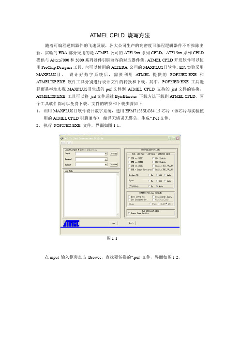
2、执行POF2JED.EXE 文件,界面如图1-1。
图1-1在input 输入框旁点击Browse,查找要转换的*.pof 文件,界面如图1-2。
图1-2在图1-2中,单击所需的*.pof 文件后会自动被添加在文件名框中,软件将根据Mamplus2 中工程的器件型号,寻找对应的ATMEL CPLD,并默认将转换的jed 文件放在与pof 文件同目录下,界面如图1-3。
3、点击图1-3中的run 开始文件转换,完成界面如图1-4。
图1-44、打开ATMELISP.EXE文档,下载jed 文件(正确连接下载线,并给下载板上电)。
界面如图1-5。

单片机烧录方法范文一、ISP烧录方法ISP(In System Programming)是一种在电路板上通过外部接口对单片机进行编程的方法。
这种方法使用的烧录器通常包括一个编程器和一个目标板接口。
具体的烧录步骤如下:1.连接编程器和目标板接口。
将编程器通过USB或串口等接口连接到计算机,并将目标板接口与目标单片机连接。
2.打开编程软件。
根据编程器的型号,打开相应的编程软件。
3.设置编程参数。
在编程软件中选择目标单片机的型号,并设置好程序文件的路径和其他相关参数。
4.擦除芯片。
在编程软件中选择擦除芯片的操作。
擦除操作会将芯片内部的所有数据清零。
5.编程。
在编程软件中选择编程操作。
编程操作会将程序文件的内容烧录到芯片的指定地址。
6.验证。
在编程软件中选择验证操作。
验证操作会读取刚刚烧录的程序,并与原程序进行比较,判断烧录是否成功。
7.完成。
如果验证成功,则表示烧录操作已完成。
如果验证失败,则需要检查连接是否正确,重新进行烧录操作。
二、JTAG烧录方法JTAG(Joint Test Action Group)是一种用于测试和调试电子设备的标准接口。
除了测试和调试,JTAG接口也可以用于单片机的烧录。
具体的烧录步骤如下:1. 连接JTAG模块和目标板接口。
将JTAG模块通过USB或Ethernet等接口连接到计算机,并将目标板接口与目标单片机连接。
2.打开JTAG编程软件。
根据JTAG模块的型号,打开相应的编程软件。
3.设置编程参数。
在编程软件中选择目标单片机的型号,并设置好程序文件的路径和其他相关参数。
4.连接调试接口。
在编程软件中选择连接调试接口的操作。
这个操作会与目标单片机建立通信连接。
5.擦除芯片。
在编程软件中选择擦除芯片的操作。
擦除操作会将芯片内部的所有数据清零。
6.编程。
在编程软件中选择编程操作。
编程操作会将程序文件的内容烧录到芯片的指定地址。
7.验证。
在编程软件中选择验证操作。
验证操作会读取刚刚烧录的程序,并与原程序进行比较,判断烧录是否成功。
——————————————————————————第十九课ATMEAG16L的内部EEPROM读写编程本教程节选自周兴华老师《手把手教你学AVR单片机C程序设计》教程,如需转载,请注明出处!读者可通过当当网、淘宝网等网站购买本教程,如需购买配书实验器材,可登陆周兴华单片机培训中心网购部自助购买!11.1 ATMEAG16L的内部EEPROMATmegal6L单片机片内有512个字节的EEPROM,它作为一个独立的数据空间存在。
ATmegal6L的EEPROM采用独立线性编址,其地址范围为0~511。
ATmegal6L通过对相关单片机培训寄存器的操作实现对EEPROM按字节进行读写。
ATmegal6L的EEPROM至少可以擦写100000次。
ATmegal6L的EEPROM的写入时间约花数毫秒,取决于VCC的电压。
电源电压越低,写周期越长。
11.2 与EEPROM相关的寄存器——————————————————————————l.EEPROM地址寄存器—EEARH、EEARLEEPROM地址寄存器EEARH、EEARL用于指定某个EEPROM单元的地址。
512个字节的EEPROM线性编址为0~511。
地址寄存器EEARH、EEARL可读可写,初始值没有定义,访问前必须赋予正确的地址。
2.EEPROM数据寄存器—EEDREEPROM数据寄存器EEDR用于存放即将写入EEPROM或者从EEPROM读出的某个单元的数据。
写入或者读出的地址由EEPROM的地址寄存器EEARH、EEARL给出。
EEPROM按字节进行读写。
EEPROM数据寄存器EEDR可读可写,初始值为0x00。
3.EEPROM控制寄存器—EECR——————————————————————————EEPROM控制寄存器EECR用于控制单片机对EEPROM的操作。
位7~4:保留位。
读这些位时总为0。
位3:EERIE位为EEPROM中断准备好使能位。
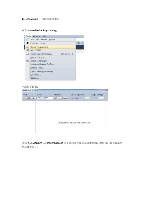
AtmelStudio6.0 下程序的烧录操作
点击tools->Device Programming
出现如下画面:
选择Tool->JTAGICE mkll070000004699,这个选项是选择仿真器类型的,根据自己的仿真器类型选择就行了。
选择Device下的下拉菜单,选择自己的单片机型号。
选择Interface下的下拉菜单,选择ISP,然后点击Apply。
依次点击Target Voltage和Device signature下的Read,此时会读出当前片子的电压和地址。
点击左边栏目中的Memories,在右侧的复选框中找到工程路径下的.hex文件,点击Program,即可将程序下载到单片机内。
下载完成后会出现如下界面:
点击Fuses,此处是对单片机熔丝位的设置,所以选择要谨慎,否则单片机会被锁。
根据自己的晶振选择系统时钟,INTRCOSC为内部时钟信号,EXTXOSC 为外部时钟信号;内部时钟信号是以单片机内部的时钟为参考,外部时钟信号是以外接晶振为参考;由于atmega88单片机内部的晶振是LC震荡,所以并不精确,因此要用到定时器或者时序等,建议用外部晶振。
选择内部晶振:
选择外部晶振:
选择完成之后点击Program ,之后会出现如下显示,表示下载完成;如果熔丝位没有更改此处就不需要点击Program,如果更改了则需要重新Program之后才能生效。
烧写程序步骤
嘿,朋友们!今天咱就来讲讲烧写程序这个事儿。
你想想看啊,烧写程序就像是给一个机器注入灵魂。
这可不是随随便便就能搞定的事儿,得有点技巧和耐心呢!
首先,咱得把准备工作做好。
就像要去打仗,你得先把武器弹药准备齐全吧!得把需要烧写的程序找出来,确认好版本啥的,可别弄错了,不然那不就成了乱弹琴啦!
然后呢,连接好设备。
这就好比是给机器搭起了一座沟通的桥梁,要是桥没搭好,那灵魂咋能送过去呢?这时候可不能粗心大意,得仔细检查好每一个接口,每一根线。
接下来就是关键时刻啦!开始烧写程序。
就好像是把珍贵的宝贝小心翼翼地放进一个特别的盒子里。
这个过程可得全神贯注,不能有一丝分心。
看着那些代码一点点地传输过去,心里还真有点小激动呢!
烧写的过程中,你可得盯着点进度条啊,就像看着赛跑的选手一点点冲向终点。
要是突然卡住了,那可别急得跳脚,得冷静下来找找原因。
是不是哪里没设置好呀,还是设备出了啥小毛病。
等烧写完成啦,别着急欢呼,还得检查检查效果呢!就像是做好了一道菜,得尝尝味道对不对。
看看程序运行得顺不顺畅,有没有啥问题。
要是有问题,那咱就得重新再来一遍咯。
你说这烧写程序是不是挺有意思的?就像一场小小的冒险,有挑战也有惊喜。
咱得胆大心细,才能把这个灵魂注入的工作完成得漂漂亮亮的呀!
总之呢,烧写程序可不能马虎,每一个步骤都得认真对待。
这就像是盖房子,基础打不好,房子可就不结实啦!所以啊,大家一定要用心去做,相信自己一定能成功的!加油吧!。
51单片机烧写方法一、引言51单片机是一种常用的单片机,广泛应用于各种电子设备中。
烧写是将程序代码写入51单片机的过程,是使用单片机的基础操作。
本文将介绍51单片机的烧写方法,帮助读者了解如何正确地进行烧写操作。
二、烧写工具准备进行51单片机的烧写操作,首先需要准备以下工具:1. 51单片机烧写器:一种专门用于将程序代码写入51单片机的设备,常见的有USB转串口烧写器和ISP烧写器两种;2. 电脑:用于连接烧写器,并通过烧写软件进行烧写操作;3. 烧写软件:根据烧写器的型号选择相应的烧写软件,常见的有STC-ISP、Flash Magic等。
三、烧写步骤1. 连接烧写器:将烧写器通过USB或串口连接到电脑上,并确保连接正常;2. 打开烧写软件:根据烧写器的型号选择相应的烧写软件,并打开软件;3. 设置烧写参数:在烧写软件中选择正确的单片机型号,并设置好烧写参数,如烧写速度、烧写模式等;4. 导入程序代码:将需要烧写的程序代码导入烧写软件中,通常是通过选择文件或拖拽文件的方式导入;5. 连接单片机:将51单片机通过编程接口连接到烧写器上,确保连接正常;6. 擦除单片机:在烧写软件中选择擦除操作,将单片机中原有的程序代码擦除,以便写入新的程序代码;7. 烧写程序代码:点击烧写软件中的烧写按钮,开始将程序代码写入单片机中;8. 等待烧写完成:等待烧写软件提示烧写完成,此时烧写操作已经完成;9. 断开连接:断开51单片机与烧写器之间的连接,完成烧写过程。
四、烧写注意事项1. 确认单片机型号:在烧写操作之前,要确认所使用的单片机型号,选择正确的烧写软件和参数设置;2. 确保连接正常:在进行烧写操作之前,要检查烧写器与电脑、单片机之间的连接是否正常,避免烧写失败;3. 备份程序代码:在擦除单片机之前,建议先备份原有的程序代码,以便需要时恢复;4. 不要中断烧写过程:在烧写过程中,不要随意中断电源或断开连接,以免造成单片机损坏;5. 验证烧写结果:在烧写完成后,可以通过读取单片机中的程序代码,与原始代码进行比对,以验证烧写结果的准确性。
AT89C51/52/55单片机编程器(烧写器)制作--------------------------------------------------------------------------------AT89C51/52/55单片机编程器(烧写器)制作AT89C51是一款应用最为广泛的8051单片机,更重要的是他具有反复烧写(FLASH)的特性。
一般情况下可重复烧写1000次,这样为初学者试验提供了一个廉价的平台。
为了满足广大单片机爱好者动手的需要,本人利用半个月的时间,参考国外资料,实际设计制作成功一款简单的AT89C51/52/55单片机编程器。
由于单片机编程时序不同,这一款编程器仅仅支持ATMEL 公司的AT89C51, AT89C52, AT89C55芯片,不支持华邦或飞利浦兼容芯片。
下面是单片机编程器电路图.注:元器件清单见附录工作原理简述:Q2, Q4以及周围的几个元件构成了电平转换电路,这样节省了1片max 232芯片,在要求不高的场合,这个电路在单片机通信中可以取代MAX232。
Q1, R2,R4,DW2,4个元件为编程器提供烧写用12V电压,其中,R4, R2构成了分压电路;平时,*芯片89C51第13脚(P3.3)输出高电平,Q1导通,R2(1K)将DW2(12V)拉低,此时DW2电压由R4,R2 分压,大约3-5V 之间;当写程序时,*芯片第13脚(P3.3)输出低电平,Q1截止,DW2(12V)直接送到被烧芯片的31脚,从而提供烧写电压。
ATMEL官方网站提供的编程器器烧写电压是用LM317调整得到的,并且用到了两个高精度电阻,电路复杂且成本高,该电路经过本人数百台的实验证明非常稳定可靠.电源变压器要求为15V的电源,例如常见的3-12V直流可调电源,注意其空载电压不要低于13V , 滤波应好一些,否则可能出现编程不可靠的情况。
*芯片用IC座安装,另外找一个编程器烧写好*程序EZ51.HEX后插入,方便调试。
Features●EE Programmable Serial Memories Designed to Store Configuration Programs forAltera ® FLEX ® and APEX ™ Field Programmable Gate Arrays (FPGA)●Supports both 3.3V and 5.0V Operating Voltage Applications ●In-System Programmable (ISP) via 2-wire Bus ●Simple Interface to SRAM FPGAs●Compatible with the Atmel ® AT6000, AT40K and AT94K Devices, Altera FLEX,APEX Devices, ORCA ® FPGAs, Xilinx ® XC3000, XC4000, XC5200, Spartan ®, Virtex ™ FPGAs, Motorola MPA1000 FPGAs●Cascadable Read-back to Support Additional Configurations or Higher-density Arrays ●Very Low-power CMOS EEPROM Process ●Programmable Reset Polarity●8-lead PDIP and 20-lead PLCC Packages (Pin-compatible Across Product Family)●Emulation of the Atmel AT24C Serial EEPROMs ●Low-power Standby Mode ●High-reliabilityEndurance: 100,000 Write CyclesData Retention: 90 Years for Industrial Parts (at 85 C)●Green (Pb/Halide-free/RoHS Compliant) Package Options AvailableDescriptionThe Atmel ® AT17LVxxxA FPGA configuration EEPROMs (Configurators) provide an easy-to-use, cost-effective configuration memory solution for FPGAs. The AT17LVxxxA are packaged in 8-lead PDIP and 20-lead PLCC options. TheAT17LVxxxA configurator uses a simple serial-access procedure to configure one or more FPGA devices. The user can select the polarity of the reset function by programming four EEPROM bytes. These devices support a write protection mechanism within its programming mode.The AT17LVxxxA configurators can be programmed with industry-standardprogrammers, the Atmel ATDH2200E Programming Kit, or the Atmel ATDH2225 ISP Cable.Table 1.AT17LVxxxA Packages65,536 x 1-bit (1)131,072 x 1-bit (1)262,144 x 1-bit (1)524,288 x 1-bit 1,048,576 x 1-bit 2,097,152 x 1-bitAT17LV65A (1), AT17LV128A (1), AT17LV256A (1)AT17LV512A, AT17LV010A, AT17LV002AFPGA Configuration EEPROM Memory3.3V and 5V System SupportDATASHEETNote 1.AT17LV65A, AT17LV128A, and AT17LV256A areNot Recommended for New Designs (NRND) and are Replaced by AT17LV512A.AT17LV65A/128A/256A/512A/002A [DATASHEET]Atmel-2322I-FPGA-AT17LV65A-128A-256A-512A-002A-Datasheet_10201421.Pin Configuration and DescriptionsTable 1-1.Pin Descriptions3AT17LV65A/128A/256A/512A/002A [DATASHEET]Atmel-2322I-FPGA-AT17LV65A-128A-256A-512A-002A-Datasheet_102014Table 1-2.Pin ConfigurationsNotes:1.The nCASC feature is not available on the AT17LV65A (NRND) device.2.The AT17LV65A, AT17LV128A, and AT17LV256A are not recommended for new designs.Figure 1-1.Pinouts (1)Notes: 1. Drawings are not to scale.2. This pin is only available on the AT17LV65A/128A/256A (NRND).3. This pin is only available on the AT17LV512A/010A/002A.4. The nCASC feature is not available on the AT17LV65A (NRND).8-lead PDIP(Top View)DATA DCLK(WP (2)) RESET/OEnCSV CC SER_EN nCASC (4) (A2)GND1234876520-lead PLCC(Top View)N CD A T AN CV C CN CSER_EN NC NCNC (READY (3))NCDCLK WP1(3)NC NC(WP (2)) RESET/OEn C SG N DN C(A 2) n C A S C (4)N C3212019910111213456781817161514AT17LV65A/128A/256A/512A/002A [DATASHEET]Atmel-2322I-FPGA-AT17LV65A-128A-256A-512A-002A-Datasheet_10201442.Block DiagramFigure 2-1.Block DiagramNotes:1.This pin is only available on AT17LV65A/128A/256A (NRND).2.This pin is only available on AT17LV512A/010A/002A.3.The nCASC feature is not available on the AT17LV65A (NRND).(WP (1))5AT17LV65A/128A/256A/512A/002A [DATASHEET]Atmel-2322I-FPGA-AT17LV65A-128A-256A-512A-002A-Datasheet_1020143.Device DescriptionThe control signals for the configuration EEPROM (nCS, RESET/OE and DCLK) interface directly with the FPGA device control signals. All FPGA devices can control the entire configuration process and retrieve data from the configuration EEPROM without requiring an external controller.The configuration EEPROM’s RESET/OE and nCS pins control the tri-state buffer on the DATA output pin and enable the address counter and the oscillator. When RESET/OE is driven Low, the configuration EEPROM resets its address counter and tri-states its DATA pin. The nCS pin also controls the output of the AT17LVxxxA configurator. If nCS is held High after the RESET/OE pulse, the counter is disabled and the DATA output pin is tri-stated. When nCS is driven subsequently Low, the counter and the DATA output pin are enabled. When RESET/OE is driven Low again, the address counter is reset and the DATA output pin is tri-stated, regardless of the state of the nCS.When the configurator has driven out all of its data and nCASC is driven Low, the device tri-states the DATA pin to avoid contention with other configurators. Upon power-up, the address counter is automatically reset.This is the default setting for the device. Since almost all FPGAs use RESET Low and OE High, this document will describe RESET/OE.4.FPGA Master Serial Mode SummaryThe I/O and logic functions of any SRAM-based FPGA are established by a configuration program. Theprogram is loaded either automatically upon power-up, or on command, depending on the state of the FPGA mode pins. In Master mode, the FPGA automatically loads the configuration program from an external memory. The AT17LVxxxA Serial Configuration EEPROM has been designed for compatibility with the Master Serial mode.This document discusses the Altera FLEX FPGA device interfaces.5.Control of ConfigurationMost connections between the FPGA device and the AT17LVxxxA Serial EEPROM are simple and self-explanatory.●The DATA output of the AT17LVxxxA configurator drives DIN of the FPGA devices.●The master FPGA DCLK output or external clock source drives the DCLK input of the AT17LVxxxA configurator.●The nCASC output of any AT17LVxxxA configurator drives the nCS input of the next configurator in a cascaded chain of EEPROMs.●SER_EN must be connected to V CC (except during ISP).AT17LV65A/128A/256A/512A/002A [DATASHEET]Atmel-2322I-FPGA-AT17LV65A-128A-256A-512A-002A-Datasheet_10201466.Cascading Serial Configuration EEPROMsFor multiple FPGAs configured as a daisy-chain, or for FPGAs requiring larger configuration memories, cascaded configurators provide additional memory.After the last bit from the first configurator is read, the next clock signal to the configurator asserts its nCASC output low and disables its DATA line driver. The second configurator recognizes the low level on its nCS input and enables its DATA output.After configuration is complete, the address counters of all cascaded configurators are reset if the RESET/OE on each configurator is driven to a Low level.If the address counters are not to be reset upon completion, then the RESET/OE input can be tied to a High level.The AT17LV65A (NRND) does not have the nCASC feature to perform cascaded configurations.7.AT17LVxxxA Reset PolarityThe AT17LVxxxA configurator allows the user to program the polarity of the RESET/OE pin as either RESET/OE or RESET/OE. This feature is supported by industry-standard programmer algorithms.8.Programming ModeThe programming mode is entered by bringing SER_EN Low. In this mode the chip can be programmed by the 2-wire serial bus. The programming is done at V CC supply only. Programming super voltages are generated inside the chip.9.Standby ModeThe AT17LVxxxA enters a low-power standby mode whenever nCS is asserted High. In this mode,the configurator consumes less than 150μA of current at 3.3V. The output remains in a high-impedance state regardless of the state of the RESET/OE input.7AT17LV65A/128A/256A/512A/002A [DATASHEET]Atmel-2322I-FPGA-AT17LV65A-128A-256A-512A-002A-Datasheet_10201410.Electrical Specifications10.1Absolute Maximum Ratings*10.2Operating ConditionsTable 10-1.Operating Conditions10.3DC CharacteristicsTable 10-2.DC Characteristics for V CC = 3.3V ± 10%Note:1.The AT17LV65A, AT17LV128A, and AT17LV256A are not recommended for new designs.Operating Temperature . . . . . . . . . . . .-40︒C to +85︒C Storage Temperature. . . . . . . . . . . . .-65︒C to +150︒C Voltage on Any Pinwith Respect to Ground . . . . . . . . .-0.1V to V CC +0.5V Supply Voltage (V CC ) . . . . . . . . . . . . . . -0.5V to +7.0V Maximum Soldering Temp. (10s @ 1/16 in.) . . .260︒C ESD (R ZAP = 1.5K, C ZAP = 100 pF)2000V*Notice:Stresses beyond those listed under AbsoluteMaximum Ratings may cause permanent damage to the device. This is a stress rating only and functional operation of the device at these or any other conditions beyond those listed underoperating conditions is not implied. Exposure to Absolute Maximum Rating conditions for extended periods of time may affect device reliability.AT17LV65A/128A/256A/512A/002A [DATASHEET]Atmel-2322I-FPGA-AT17LV65A-128A-256A-512A-002A-Datasheet_1020148Table 10-3.DC Characteristics for V CC = 5.0V ± 10%Note:1.The AT17LV65A, AT17LV128A, and AT17LV256A are not recommended for new designs.10.4AC CharacteristicsTable 10-4.AC Characteristics for V CC = 3.3V ± 10%Notes:1.AC test lead = 50pF.2.Float delays are measured with 5pF AC loads. Transition is measured ± 200mV from steady-state active levels.3.The AT17LV65A, AT17LV128A, and AT17LV256A are not recommended for new designs.9AT17LV65A/128A/256A/512A/002A [DATASHEET]Atmel-2322I-FPGA-AT17LV65A-128A-256A-512A-002A-Datasheet_102014Notes:1.AC test lead = 50pF.2.Float delays are measured with 5pF AC loads. Transition is measured ± 200mV from steady-state active levels.3.The AT17LV65A, AT17LV128A, and AT17LV256A are not recommended for new designs.Table 10-6.AC Characteristics for V CC = 5.0V ± 10%Notes:1.AC test lead = 50pF.2.Float delays are measured with 5pF AC loads. Transition is measured ± 200mV from steady-state active levels.3.The AT17LV65A, AT17LV128A, and AT17LV256A are not recommended for new designs.AT17LV65A/128A/256A/512A/002A [DATASHEET]Atmel-2322I-FPGA-AT17LV65A-128A-256A-512A-002A-Datasheet_10201410Notes:1.AC test lead = 50pF.2.Float delays are measured with 5pF AC loads. Transition is measured ± 200mV from steady-state active levels.3.The AT17LV65A, AT17LV128A, and AT17LV256A are not recommended for new designs.Figure 10-1.AC WaveformsFigure 10-2.AC Waveforms when CascadingnCSRESET/OEDCLKDATAnCSRESET/OEDCLKDATAnCASL11AT17LV65A/128A/256A/512A/002A [DATASHEET]Atmel-2322I-FPGA-AT17LV65A-128A-256A-512A-002A-Datasheet_10201410.5Thermal Resistance CoefficientsTable 10-8.Thermal Resistance CoefficientsNotes:1.Airflow = 0ft/min.2.The AT17LV65A, AT17LV128A, and AT17LV256A are not recommended for new designs.AT17LV65A/128A/256A/512A/002A [DATASHEET]Atmel-2322I-FPGA-AT17LV65A-128A-256A-512A-002A-Datasheet_1020141211.1Ordering Code Detail11.2Ordering InformationNotes:e 512-Kbit density parts to replace Altera EPC1441.e 1-Mbit density parts to replace Altera EPC1e 2-Mbit density parts to replace Altera EPC2.4.The AT17LVxxxA do not support JTAG programming. They use a 2-wire serial interface for in-system programming.A T 17L V 512A -10P UAtmel DesignatorProduct FamilyDevice DensitySpecial PinoutsProduct Variation65 = 65 kilobit 128 = 128 kilobit 256 = 256 kilobit 512 = 512 kilobit010 = 1 Mbit 002 = 2 MbitA = AlteraBlank = Xilinx/Atmel/Other17LV = FPGA EEPROM Configuration MemoryPackage Device GradeU = Green, Industrial Temperature Range (-40°C to +85°C)10 = Default ValuePackage OptionP = 8P3, 8-lead PDIP J =20J, 20-lead PLCC12.18P3 – PDIPAT17LV65A/128A/256A/512A/002A [DATASHEET]13Atmel-2322I-FPGA-AT17LV65A-128A-256A-512A-002A-Datasheet_102014AT17LV65A/128A/256A/512A/002A [DATASHEET]Atmel-2322I-FPGA-AT17LV65A-128A-256A-512A-002A-Datasheet_1020141412.220J – PLCC15AT17LV65A/128A/256A/512A/002A [DATASHEET]Atmel-2322I-FPGA-AT17LV65A-128A-256A-512A-002A-Datasheet_10201413.Revision HistoryX X X X X XAtmel Corporation1600 Technology Drive, San Jose, CA 95110 USAT: (+1)(408) 441.0311F: (+1)(408) 436.4200|© 2014 Atmel Corporation. / Rev.: Atmel-2322I-FPGA-AT17LV65A-128A-256A-512A-002A-Datasheet_102014.Atmel ®, Atmel logo and combinations thereof, Enabling Unlimited Possibilities ®, and others are registered trademarks or trademarks of Atmel Corporation in U.S. and other countries. Other terms and product names may be trademarks of others.DISCLAIMER: The information in this document is provided in connection with Atmel products. No license, express or implied, by estoppel or otherwise, to any intellectual property right is granted by this document or in connection with the sale of Atmel products. EXCEPT AS SET FORTH IN THE ATMEL TERMS AND CONDITIONS OF SALES LOCATED ON THE ATMEL WEBSITE, ATMEL ASSUMES NO LIABILITY WHATSOEVER AND DISCLAIMS ANY EXPRESS, IMPLIED OR STATUTORY WARRANTY RELATING TO ITS PRODUCTS INCLUDING, BUT NOT LIMITED TO, THE IMPLIED WARRANTY OF MERCHANTABILITY, FITNESS FOR A PARTICULAR PURPOSE, OR NON-INFRINGEMENT. IN NO EVENT SHALL ATMEL BE LIABLE FOR ANY DIRECT, INDIRECT, CONSEQUENTIAL, PUNITIVE, SPECIAL OR INCIDENTAL DAMAGES (INCLUDING, WITHOUT LIMITATION, DAMAGES FOR LOSS AND PROFITS, BUSINESS INTERRUPTION, OR LOSS OF INFORMATION) ARISING OUT OF THE USE OR INABILITY TO USE THIS DOCUMENT, EVEN IF ATMEL HAS BEEN ADVISED OF THE POSSIBILITY OF SUCH DAMAGES. Atmel makes no representations or warranties with respect to the accuracy or completeness of the contents of this document and reserves the right to make changes to specifications and products descriptions at any time without notice. Atmel does not make any commitment to update the information contained herein. Unless specifically provided otherwise, Atmel products are not suitable for, and shall not be used in, automotive applications. Atmel products are not intended,authorized, or warranted for use as components in applications intended to support or sustain life.SAFETY-CRITICAL, MILITARY, AND AUTOMOTIVE APPLICATIONS DISCLAIMER: Atmel products are not designed for and will not be used in connection with any applications where the failure of such products would reasonably be expected to result in significant personal injury or death (“Safety-Critical Applications”) without an Atmel officer's specific written consent. Safety-Critical Applications include, without limitation, life support devices and systems, equipment or systems for the operation of nuclear facilities and weapons systems.Atmel products are not designed nor intended for use in military or aerospace applications or environments unless specifically designated by Atmel as military-grade. Atmel products are not designed nor intended for use in automotive applications unless specifically designated by Atmel as automotive-grade.。