基于ADF4360-1的2.4G频率合成器设计
- 格式:doc
- 大小:35.00 KB
- 文档页数:5

图3 输出频谱
进行相位噪声测试,仪表选用底噪较好的噪声仪安捷伦E4443A,将单板和仪表良好接地后,设置噪声仪SPAN=200KHz,在频偏100KHz处测得相位噪声≤-115dBc/Hz,满足目标。
4 结论
本文讲述了以锁相环芯片ADF4001BRU为核心的电路设计,实现了单频点32.768MHz的信号输出,信号幅度、稳定度、相位噪声符合需求。
该电路结构简单,功耗少,体积小,便于调试,在无线通信系统中得到广泛应用。
参考文献:
[1] 远坂俊昭.锁相环(PLL)电路设计与应用 [M].何希才,译.北京:科学出版社,2006.
[2] 张雪.基于ADF4351低噪声频率合成器设计与实现[J].科技展望,2015.
[3] 李页瑞.基于ADF4350锁相频率合成器的频率源设计与实现 [J].电子技术应用,2016.
作者简介:董小丽(1985-),女,汉族,河南濮阳人,通信工程师,射频电路设计师,哈尔滨理工大学硕士研究生。
研究方向:射频电路设计。
[3] 张上均.如何提高电路板设计与制作能力的探讨 [J].科技信息,2012(29):192+229.
[4] 郭睿涵,张军元.浅谈印制电路板设计基础 [J].橡塑技术与装备,2015,41(20):74-75.。
基于ADF4360-1的本振源设计作者:邹玲石小磊来源:《现代电子技术》2009年第21期摘要:结合锁相频率合成基本原理以及高集成锁相频率合成芯片ADF4360-1工作特性,设计一个稳定的2.33 GHz本振源电路模块,应用于中频射频发信机中。
详细介绍了核心芯片的结构、原理及应用,并给出完整的硬件电路。
经仿真测试,该电路的性能指标基本符合要求。
关键词:锁相环频率合成;ADF4360-1;本振;环路滤波器中图分类号:TN742 文献标识码:A文章编号:1004-373X(2009)21-071-03Design of Clock Signal Generator Based on ADF4360-1ZOU Ling,SHI Xiaolei(School of Electrical and Electronic Engineering,Hubei University ofTechnology,Wuhan,430068,China)Abstract:The principle of phase locked loop and the performance characteristics of fully integrated voltage-controlled oscillator ADF4360-1 are analyzed.A design of a stedy 2.33 GHz local oscillator signal generator circuit module is applied to the system of Intermediate Frequency(IF).The paper elaborates on the structure,performance and application of the core chip,designs the hardware circuit.The simulation and measure of the system show that the result is correct basically.Keywords:PLL frequency synthesis;ADF4360-1;local oscillation;loop filter0 引言在无线通信领域,本振信号性能的优劣是影响混频器输出频谱纯度的主要因素。
8~12.4GHz宽带频率合成器的设计何恭涛;钱光弟【摘要】研究采用将ADI公司的ADF4350频率合成芯片输出信号多次倍频的方法来实现X波段的频率合成器.ADF4350频率合成器具有内置片上VCO(压控振荡器)和PLL(锁相环),集成度高、相位噪声低,工作频带宽,广泛用于无线电基础设备及测试设备,无线LAN,CATV和时钟发生器中.该频率合成器输出频率范围8~12.4G,频率步进50 MHz,相位噪声低于-75 dBc@10 kHz.【期刊名称】《实验科学与技术》【年(卷),期】2011(009)001【总页数】3页(P9-10,72)【关键词】倍频器;ADF4350;频率合成器;锁相环【作者】何恭涛;钱光弟【作者单位】电子科技大学自动化工程学院,成都,610054;电子科技大学自动化工程学院,成都,610054【正文语种】中文【中图分类】TN74频率合成器是以一个高精确度和高稳定度的标准频率信号作参考,经过混频、倍频与分频等,对它进行加、减、乘、除运算,最终得到和参考源具有同样精确度和稳定度的所需频率信号。
目前,频率合成器已成为通信设备、电子对抗、雷达、精密测量仪器的重要部件[1-2]。
要求设计一个输出频率 8~12.4GHz;频率步进:50MHz;输出杂散:-55 dBc;输出功率:≥15mW;输出相噪:≤-75 dBc∕ Hz@10kHz的频率合成器。
一般说来,频率合成器主要分为锁相频率合成器和直接数字频率合成器DDS2种。
锁相频率合成器是基于对参考信号频率和输出信号频率分频鉴相的原理工作,常用方案是以锁相环芯片为基础,如PE3236、PE3336、LMX2325、ADF4106,配合压控振荡器和分频器、倍频器、混频器等组成[3-5]。
由于输出频率高,频率范围大,如果采用直接分频器合成方案,分频比大,且 X波段的压控振荡器价格昂贵。
经比较,选择 AD I公司的ADF4350锁相环芯片,再多次倍频来实现该频率合成器。
频率合成器的设计改进
乐家骝
【期刊名称】《中原通信技术》
【年(卷),期】1993(000)001
【总页数】6页(P49-54)
【作者】乐家骝
【作者单位】无
【正文语种】中文
【中图分类】TN74
【相关文献】
1.直接数字频率合成器镜像频率的应用 [J], 陈瑞龙;于航
2.基于ADF4350锁相频率合成器的频率源设计与实现 [J], 徐述武;汪海勇;唐云峰
3.超声波频率跟踪系统中频率合成器的设计 [J], 崔瑞雪;王俊红;张洁
4.全向信标频率合成器参考频率故障分析 [J], 李文凯; 雷斯元
5.一种用于频率合成器的自动频率校正电路 [J], 邹奇峰;雷旭;廖鹏飞
因版权原因,仅展示原文概要,查看原文内容请购买。
0引言锁相(PhaseLock)技术是一种相位负反馈频率控制技术,该技术在锁定时无剩余频差,并具有良好的窄带载波跟踪性能和带宽调制跟踪性能,而且对相位噪声和杂散也具有很好的抑制作用。
因此,通过锁相频率合成技术实现的频率源已在通信、电视等领域得了广泛应用。
本文介绍的ADl 公司的ADF4360系列芯片就是用于无线通信射频系统(GSM,DECT,PCS,WCDMA。
DCS)基站和WLAN混频电路的一款性价比很高,且应用范围较广的锁相芯片。
1ADF4360_4的性能特点ADF4360_4丰要由数字鉴相器、电荷泵、R分频器、A,B计数器及双模前置P/P+1分频器等组成。
数字鉴相器对R计数器与N计数器的输出信号进行相位比较,得到一个误差电压。
14bit可编程参考R分频器对外部晶振分频后得到参考频率。
该器件可以通过可编程6位A计数器、13位B计数器及双模前置分频器(P/P+1)来共同完成主分频比N(N=BP+A)。
因此,设计时只需外加环路滤波器,并选择合适的参考值,即可获得稳定的频率输出,其输出频率为:f0=fvco=N(fi/R)式中,fi为参考频率,它可由高稳定度晶体振荡器提供。
而其鉴相频率fr为:fr=fi/R其中,fi应小于8MHz。
ADF4360_4是美国ADI公司生产的的高性能锁相频率合成芯片,主要用于无线发射机和接收机中为上下变频提供本振信号。
该器件的主要特点如下:(1)该合成器的输出频率范围为1450~1750MHz;并可选择二分频。
选择二分频时,可输出725~875MHz的频率信号;(2)工作电压为3~3.6V;(3)合成器的输出信号的功率可控制范围为-13~-4dbm;(4)可编程双模前置分频器的分频比为8/9、16/17、32/33等;(5)能够进行模拟和数字锁定检测;(6)芯片内部集成又VCO。
ADF4360_4是一款双模前置分频型单环频率合成器,该器件可在不改变频率分辨率的同时,有效地提高频率合成器的输山频率。
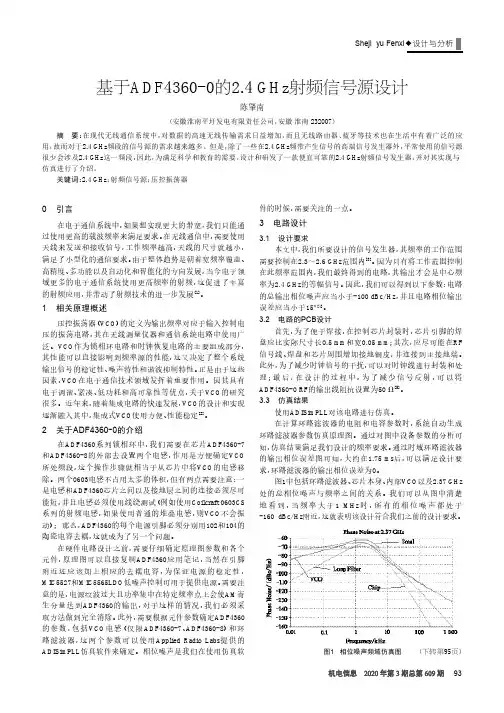
基于ADF4360-0的2.4GHz射频信号源设计陈肇南(安徽淮南平圩发电有限责任公司,安徽淮南232007)摘要:在现代无线通信系统中,对数据的高速无线传输需求日益增加,而且无线路由器、蓝牙等技术也在生活中有着广泛的应用,故而对于2.4GHz频段的信号源的需求越来越多。
但是,除了一些在2.4GHz频带产生信号的高端信号发生器外,平常使用的信号源很少会涉及2.4GHz这一频段,因此,为满足科学和教育的需要,设计和研发了一款便宜可靠的2.4GHz射频信号发生器,并对其实现与仿真进行了介绍。
关键词:2.4GHz;射频信号源;压控振荡器0引言在电子通信系统中,如果想实现更大的带宽,我们只能通过使用更高的载波频率来满足要求。
在无线通信中,需要使用天线来发送和接收信号,工作频率越高,天线的尺寸就越小,满足了小型化的通信要求。
由于整体趋势是朝着宽频率覆盖、高精度、多功能以及自动化和智能化的方向发展,当今电子领域更多的电子通信系统使用更高频率的射频,这促进了丰富的射频应用,并带动了射频技术的进一步发展[1]。
1相关原理概述压控振荡器(VCO)的定义为输出频率对应于输入控制电压的振荡电路,其在无线测量仪器和通信系统电路中使用广泛。
VCO作为锁相环电路和时钟恢复电路的主要组成部分,其性能可以直接影响到频率源的性能,这又决定了整个系统输出信号的稳定性、噪声特性和谐波抑制特性。
正是由于这些因素,VCO在电子通信技术领域发挥着重要作用。
因其具有电子调谐、紧凑、低功耗和高可靠性等优点,关于VCO的研究很多。
近年来,随着集成电路的快速发展,VCO的设计和实现逐渐融入其中,集成式VCO使用方便、性能稳定[2]。
2关于ADF4360-0的介绍在ADF4360系列锁相环中,我们需要在芯片ADF4360-7和ADF4360-8的外部去设置两个电感,作用是方便确定VCO 所处频段,这个操作步骤就相当于从芯片中将VCO的电感移除。
两个0603电感不占用太多的体积,但有两点需要注意:一是电感和ADF4360芯片之间以及接地层之间的连接必须尽可能短,并且电感必须使用线绕测试(例如使用Coilcraft0603CS 系列的射频电感,如果使用普通的堆叠电感,则VCO不会振动);那么,ADF4360的每个电源引脚必须分别用102和104的陶瓷电容去耦,这就成为了另一个问题。
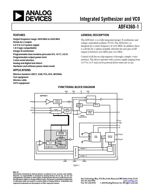
Integrated Synthesizer and VCOADF4360-1 Rev.BInformation furnished by Analog Devices is believed to be accurate and reliable.However, no responsibility is assumed by Analog Devices for its use, nor for anyinfringements of patents or other rights of third parties that may result from its use. Specifications subject to change without notice. No license is granted by implication or otherwise under any patent or patent rights of Analog Devices. Trademarks and registered trademarks are the property of their respective owners.One Technology Way, P.O. Box 9106, Norwood, MA 02062-9106, U.S.A. Tel: Fax: 781.326.8703© 2004 Analog Devices, Inc. All rights reserved.FEATURESOutput frequency range: 2050 MHz to 2450 MHzDivide-by-2 output3.0 V to 3.6 V power supply1.8 V logic compatibilityInteger-N synthesizerProgrammable dual-modulus prescaler 8/9, 16/17, 32/33 Programmable output power level3-wire serial interfaceAnalog and digital lock detectHardware and software power-down mode APPLICATIONSWireless handsets (DECT, GSM, PCS, DCS, WCDMA)Test equipmentWireless LANsCATV equipment GENERAL DESCRIPTIONThe ADF4360-1 is a fully integrated integer-N synthesizer and voltage-controlled oscillator (VCO). The ADF4360-1 is designed for a center frequency of 2250 MHz. In addition, there is a divide-by-2 option available, whereby the user gets an RF output of between 1025 MHz and 1225 MHz.Control of all the on-chip registers is through a simple 3-wire interface. The device operates with a power supply ranging from 3.0 V to 3.6 V and can be powered down when not in use.FUNCTIONAL BLOCK DIAGRAMCPVCO REFTUNEC CC NOUT AOUT BFigure 1.ADF4360-1Rev. B | Page 2 of 24TABLE OF CONTENTSSpecifications.....................................................................................3 Timing Characteristics.....................................................................5 Absolute Maximum Ratings............................................................6 Transistor Count...........................................................................6 ESD Caution..................................................................................6 Pin Configuration and Function Descriptions.............................7 Typical Performance Characteristics.............................................8 Circuit Description...........................................................................9 Reference Input Section...............................................................9 Prescaler (P/P + 1)........................................................................9 A and B Counters.........................................................................9 R Counter......................................................................................9 PFD and Charge Pump................................................................9 MUXOUT and Lock Detect......................................................10 Input Shift Register.....................................................................10 VCO.............................................................................................10 Output Stage................................................................................11 Latch Structure...........................................................................12 Power-Up.....................................................................................16 Control Latch..............................................................................18 N Counter Latch.........................................................................19 R Counter Latch.........................................................................19 Applications.....................................................................................20 Direct Conversion Modulator..................................................20 Fixed Frequency LO...................................................................21 Interfacing...................................................................................21 PCB Design Guidelines for Chip-Scale Package..........................22 Output Matching........................................................................22 Outline Dimensions.......................................................................23 Ordering Guide.. (23)REVISION HISTORY12/04—Rev. A to Rev. BUpdated Format..................................................................Universal Changes to Specifications................................................................3 Changes to the Timing Characteristics.........................................5 Changes to the Power-Up Section................................................16 Added Table 10...............................................................................16 Added Figure 16..............................................................................16 Changes to Ordering Guide..........................................................23 Updated Outline Dimensions. (23)6/04—Data Sheet Changed from Rev. 0 to Rev. AChanges to Specifications................................................................3 Changes to Table 6..........................................................................12 Changes to Table 7..........................................................................13 Changes to Table 9.. (15)8/03—Revision 0: Initial VersionADF4360-1Rev. B | Page 3 of 24SPECIFICATIONS 1AV DD = DV DD = V VCO = 3.3 V ± 10%; AGND = DGND = 0 V; T A = T MIN to T MAX , unless otherwise noted. Table 1.Parameter B Version Unit Conditions/Comments REF IN CHARACTERISTICS REF IN Input Frequency 10/250 MHz min/max For f < 10 MHz, use a dc-coupled CMOS compatiblesquare wave, slew rate > 21 V/µs.REF IN Input Sensitivity 0.7/AV DD p-p min/max AC-coupled. 0 to AV DD V max CMOS compatible. REF IN Input Capacitance 5.0 pF max REF IN Input Current ±100 µA max PHASE DETECTORPhase Detector Frequency 28 MHz max CHARGE PUMPI CP Sink/Source 3With R SET = 4.7 kΩ. High Value 2.5 mA typ Low Value 0.312 mA typ R SET Range 2.7/10 kΩ I CP 3-State Leakage Current 0.2 nA typ Sink and Source Current Matching 2 % typ 1.25 V ≤ V CP ≤ 2.5 V. I CP vs. V CP 1.5 % typ 1.25 V ≤ V CP ≤ 2.5 V. I CP vs. Temperature 2 % typ V CP = 2.0 V. LOGIC INPUTS V INH , Input High Voltage 1.5 V min V INL , Input Low Voltage 0.6 V max I INH /I INL , Input Current ±1 µA max C IN , Input Capacitance 3.0 pF max LOGIC OUTPUTS V OH , Output High Voltage DV DD – 0.4 V min CMOS output chosen. I OH , Output High Current 500 µA max V OL , Output Low Voltage 0.4 V max I OL = 500 µA. POWER SUPPLIES AV DD 3.0/3.6 V min/V max DV DD AV DD V VCO AV DD AI DD 410 mA typDI DD 4 2.5 mA typ I VCO 4, 524.0 mA typ I CORE = 15 mA.I RFOUT 43.5 – 11.0 mA typ RF output stage is programmable.Low Power Sleep Mode 47 µA typ RF OUTPUT CHARACTERISTICS 5 VCO Output Frequency 2050/2450 MHz min/max I CORE = 15 mA. VCO Sensitivity 57 MHz/V typ Lock Time 6400 µs typ To within 10 Hz of final frequency. Frequency Pushing (Open Loop) 6 MHz/V typ Frequency Pulling (Open Loop) 15 kHz typ Into 2.00 VSWR load. Harmonic Content (Second) −20 dBc typ Harmonic Content (Third) −35 dBc typOutput Power 5, 7−13/−6 dBm typ Programmable in 3 dB steps. See Table 7. Output Power Variation ±3 dB typ For tuned loads, see the Output Matching section. VCO Tuning Range 1.25/2.5 V min/maxADF4360-1Rev. B | Page 4 of 24Parameter B Version Unit Conditions/CommentsNOISE CHARACTERISTICS 1, 5VCO Phase-Noise Performance 8 −110 dBc/Hz typ @ 100 kHz offset from carrier. −130 dBc/Hz typ @ 1 MHz offset from carrier. −141 dBc/Hz typ @ 3 MHz offset from carrier. −148 dBc/Hz typ @ 10 MHz offset from carrier.Synthesizer Phase-Noise Floor 9−172 dBc/Hz typ @ 25 kHz PFD frequency. −163 dBc/Hz typ @ 200 kHz PFD frequency. −147 dBc/Hz typ @ 8 MHz PFD frequency. In-Band Phase Noise 10, 11−81 dBc/Hz typ @ 1 kHz offset from carrier.RMS Integrated Phase Error 120.72 Degrees typ 100 Hz to 100 kHz.Spurious Signals due to PFD Frequency 11, 13−70 dBc typ Level of Unlocked Signal with MTLD Enabled −38 dBm typ1 Operating temperature range is –40°C to +85°C.2Guaranteed by design. Sample tested to ensure compliance. 3I CP is internally modified to maintain constant-loop gain over the frequency range. 4T A = 25°C; AV DD = DV DD = V VCO = 3.3 V; P = 32. 5These characteristics are guaranteed for VCO Core Power = 15 mA. 6Jumping from 2.05 GHz to 2.45 GHz. PFD frequency = 200 kHz; loop bandwidth = 10 kHz. 7Using 50 Ω resistors to V VCO into a 50 Ω load. For tuned loads, see the section. Output Matching 8The noise of the VCO is measured in open-loop conditions. 9The synthesizer phase-noise floor is estimated by measuring the in-band phase noise at the output of the VCO and subtracting 20 log N (where N is the N divider value). 10The phase noise is measured with the EVAL-ADF4360-xEB1 Evaluation Board and the HP8562E Spectrum Analyzer. The spectrum analyzer provides the REF IN for the synthesizer; offset frequency = 1 kHz. 11f REFIN = 10 MHz; f PFD = 200 kHz; N = 12500; Loop B/W = 10 kHz. 12f REFIN = 10 MHz; f PFD = 1 MHz; N = 2400; Loop B/W = 25 kHz. 13The spurious signals are measured with the EVAL-ADF4360-xEB1 Evaluation Board and the HP8562E Spectrum Analyzer. The spectrum analyzer provides the REF IN for the synthesizer; f REFOUT = 10 MHz @ 0 dBm.ADF4360-1Rev. B | Page 5 of 24TIMING CHARACTERISTICS 1AV DD = DV DD = V VCO = 3.3 V ± 10%; AGND = DGND = 0 V; 1.8 V and 3 V logic levels used; T A = T MIN to T MAX , unless otherwise noted. Table 2.Parameter Limit at T MIN to T MAX (B Version) Unit Test Conditions/Comments t 1 20 ns min LE Setup Timet 2 10 ns min DATA to CLOCK Setup Time t 3 10 ns min DATA to CLOCK Hold Time t 4 25 ns min CLOCK High Duration t 5 25 ns min CLOCK Low Duration t 6 10 ns min CLOCK to LE Setup Time t 720ns minLE Pulse Width1See the section for the recommended power-up procedure for this device.Power-UpCLOCKDATALELEFigure 2. Timing DiagramADF4360-1Rev. B | Page 6 of 24ABSOLUTE MAXIMUM RATINGST A = 25°C, unless otherwise noted. Table 3.Parameter Rating AV DD to GND 1−0.3 V to +3.9 V AV DD to DV DD −0.3 V to +0.3 V V VCO to GND −0.3 V to +3.9 V V VCO to AV DD −0.3 V to +0.3 V Digital I/O Voltage to GND −0.3 V to V DD + 0.3 V Analog I/O Voltage to GND −0.3 V to V DD + 0.3 VREF IN to GND −0.3 V to V DD + 0.3 VOperating Temperature RangeMaximum Junction Temperature 150°CCSP θJA Thermal Impedance(Paddle Soldered) 50°C/W (Paddle Not Soldered) 88°C/W Lead Temperature, SolderingVapor Phase (60 sec) 215°C Infrared (15 sec) 220°C1GND = AGND = DGND = 0 V.Stresses above those listed under Absolute Maximum Ratingsmay cause permanent damage to the device. This is a stress rat-ing only; functional operation of the device at these or any other conditions above those indicated in the operational sec-tions of this specification is not implied. Exposure to absolutemaximum rating conditions for extended periods may affect device reliability. This device is a high performance RF integrated circuit with an ESD rating of <1 kV and it is ESD sensitive. Proper precautions should be taken for handling and assembly.TRANSISTOR COUNT 12543 (CMOS) and 700 (Bipolar)ESD CAUTIONESD (electrostatic discharge) sensitive device. Electrostatic charges as high as 4000 V readily accumulateon the human body and test equipment and can discharge without detection. Although this product features proprietary ESD protection circuitry, permanent damage may occur on devices subjected to high energy elec-trostatic discharges. Therefore, proper ESD precautions are recommended to avoid performance degradation or loss of functionality.ADF4360-1Rev. B | Page 7 of 24PIN CONFIGURATION AND FUNCTION DESCRIPTIONSCPGND AV DD AGND RF OUT A RF OUT B V VCO DATA CLK REF IN DGND C N R SETV T U N E A G N D A G N D A G N D A G N D C C C PC EA G N DD V D DM U X O U TL E04414-003Figure 3. Pin ConfigurationADF4360-1Rev. B | Page 8 of 24TYPICAL PERFORMANCE CHARACTERISTICSFREQUENCY OFFSET (Hz)O U T P U T P O W E R (d B )Figure 4. Open Loop VCO Phase Noise04414-005–145–150–155–140–135–130–125–120–115–110–105–90–95–100–85–80–75–7010010M1M 100k10k 1000FREQUENCY OFFSET (Hz)O U T P U T P O W E R (d B )Figure 5. VCO Phase Noise, 2250 MHz, 200 kHz PFD, 10 kHz Loop Bandwidth04414-006–145–150–155–140–135–130–125–120–115–110–105–90–95–100–85–80–75–7010010M1M 100k10k 1000FREQUENCY OFFSET (Hz)O U T P U T P O W E R (d B )Figure 6. VCO Phase Noise, 1125 MHz,Divide-by-2 Enabled, 200 kHz PFD, 10 kHz Loop BandwidthO U T P U T P O W E R (d B )–2kHz –1kHz 2250MHz 1kHz 2kHzFigure 7. Close-In Phase Noise at 2250 MHz (200 kHz Channel Spacing)O U T P U T P O W E R (d B )–200kHz–100kHz2250MHz100kHz200kHzFigure 8. Reference Spurs at 2250 MHz(200 kHz Channel Spacing, 10 kHz Loop Bandwidth)O U T P U T P O W E R (d B )–90–80–70–60–50–40–30–20–100–1MHz–0.5MHz2250MHz0.5MHz1MHzFigure 9. Reference Spurs at 2250 MHz(1 MHz Channel Spacing, 25 kHz Loop Bandwidth)ADF4360-1Rev. B | Page 9 of 24CIRCUIT DESCRIPTIONREFERENCE INPUT SECTIONThe reference input stage is shown in Figure 10. SW1 and SW2 are normally closed switches. SW3 is normally open. When power-down is initiated, SW3 is closed, and SW1 and SW2 are opened. This ensures that there is no loading of the REF IN pin on power-down.04414-010POWER-DOWNFigure 10. Reference Input StagePRESCALER (P/P + 1)The dual-modulus prescaler (P/P + 1), along with the A and B counters, enables the large division ratio, N , to be realized (N = BP + A). The dual-modulus prescaler, operating at CML levels, takes the clock from the VCO and divides it down to a manage-able frequency for the CMOS A and B counters. The prescaler is programmable. It can be set in software to 8/9, 16/17, or 32/33 and is based on a synchronous 4/5 core. There is a minimum divide ratio possible for fully contiguous output frequencies; this minimum is determined by P , the prescaler value, and is given by (P 2−P).A ANDB COUNTERSThe A and B CMOS counters combine with the dual-modulus prescaler to allow a wide range division ratio in the PLL feed-back counter. The counters are specified to work when the prescaler output is 300 MHz or less. Thus, with a VCOfrequency of 2.5 GHz, a prescaler value of 16/17 is valid, but a value of 8/9 is not valid.Pulse Swallow FunctionThe A and B counters, in conjunction with the dual-modulus prescaler, make it possible to generate output frequencies that are spaced only by the reference frequency divided by R. The VCO frequency equation is()R f A B P f REFIN VCO /×]+×[=where:f VCO is the output frequency of the VCO.P is the preset modulus of the dual-modulus prescaler (8/9, 16/17, and so on).B is the preset divide ratio of the binary 13-bit counter (3 to 8191). A is the preset divide ratio of the binary 5-bit swallow counter (0 to 31). f REFIN is the external reference frequency oscillator.Figure 11. A and B CountersR COUNTERThe 14-bit R counter allows the input reference frequency to be divided down to produce the reference clock to the phase frequency detector (PFD). Division ratios from 1 to 16,383 are allowed.PFD AND CHARGE PUMPThe PFD takes inputs from the R counter and N counter(N = BP + A) and produces an output proportional to the phase and frequency difference between them. Figure 12 is a simpli-fied schematic. The PFD includes a programmable delay ele-ment that controls the width of the antibacklash pulse. This pulse ensures that there is no dead zone in the PFD transfer function and minimizes phase noise and reference spurs. Two bits in the R counter latch, ABP2 and ABP1, control the width of the pulse (see Table 9).04414-012Figure 12. PFD Simplified Schematic and Timing (In Lock)ADF4360-1Rev. B | Page 10 of 24MUXOUT AND LOCK DETECTThe output multiplexer on the ADF4360 family allows the user to access various internal points on the chip. The state of MUXOUT is controlled by M3, M2, and M1 in the function latch. The full truth table is shown in Table 7. Figure 13 shows the MUXOUT section in block diagram form.Lock DetectMUXOUT can be programmed for two types of lock detect: digital and analog. Digital lock detect is active high. When LDP in the R counter latch is set to 0, digital lock detect is set high when the phase error on three consecutive phase detector cycles is less than 15 ns.With LDP set to 1, five consecutive cycles of less than 15 ns phase error are required to set the lock detect. It stays set high until a phase error greater than 25 ns is detected on any subse-quent PD cycle.The N-channel open-drain analog lock detect should be oper-ated with an external pull-up resistor of 10 kΩ nominal. When lock has been detected, the output will be high with narrow low-going pulses.DGNDMUXOUTDV ANALOG LOCK DETECT SDOUT04414-013Figure 13. MUXOUT CircuitINPUT SHIFT REGISTERThe ADF4360 family’s digital section includes a 24-bit input shift register, a 14-bit R counter, and an 18-bit N counter, com-prising of a 5-bit A counter and a 13-bit B counter. Data isclocked into the 24-bit shift register on each rising edge of CLK. The data is clocked in MSB first. Data is transferred from the shift register to one of four latches on the rising edge of LE. The destination latch is determined by the state of the two control bits (C2, C1) in the shift register. The two LSBs are DB1 and DB0, as shown in Figure 2.The truth table for these bits is shown in Table 5. Table 6 shows a summary of how the latches are programmed. Note that the test mode latch is used for factory testing and should not be programmed by the user.Table 5. C2 and C1 Truth TableControl BitsC2 C1 Data Latch 0 0 Control Latch 0 1 R Counter1 0 N Counter (A and B) 11Test Mode LatchVCOThe VCO core in the ADF4360 family uses eight overlapping bands, as shown in Figure 14, to allow a wide frequency range to be covered without a large VCO sensitivity (K V ) and resultant poor phase noise and spurious performance.The correct band is chosen automatically by the band select logic at power-up or whenever the N counter latch is updated. It is important that the correct write sequence be followed at power-up. This sequence is 1. R counter latch 2. Control latch 3. N counter latchDuring band select, which takes five PFD cycles, the VCO V TUNE is disconnected from the output of the loop filter and connected to an internal reference voltage.04414-0140.40.20.60.81.01.21.41.61.82.42.22.02.62.83.01850190019502000205021002150220022502300235024002450250025502600FREQUENCY (MHz)V O L T A G E (V )Figure 14. Frequency vs. V TUNE , ADF4360-1The R counter output is used as the clock for the band select logic and should not exceed 1 MHz. A programmable divider is provided at the R counter input to allow division by 1, 2, 4, or 8 and is controlled by Bits BSC1 and BSC2 in the R counter latch. Where the required PFD frequency exceeds 1 MHz, the divide ratio should be set to allow enough time for correct band selection.After band select, normal PLL action resumes. The nominal value of K V is 57 MHz/V or 28 MHZ/V if divide-by-2 operation has been selected (by programming DIV2 [DB22], high in the N counter latch). The ADF4360 family contains linearization circuitry to minimize any variation of the product of I CP and K V.The operating current in the VCO core is programmable in four steps: 5 mA, 10 mA, 15 mA, and 20 mA. This is controlled by Bits PC1 and PC2 in the control latch.OUTPUT STAGEThe RF OUT A and RF OUT B pins of the ADF4360 family are con-nected to the collectors of an NPN differential pair driven by buffered outputs of the VCO, as shown in Figure 15. To allow the user to optimize the power dissipation versus the output power requirements, the tail current of the differential pair is programmable via Bits PL1 and PL2 in the control latch. Four current levels may be set: 3.5 mA, 5 mA, 7.5 mA, and 11 mA. These levels give output power levels of −13 dBm, −10.5 dBm, −8 dBm, and −6 dBm, respectively, using a 50 Ω resistor to V DD and ac coupling into a 50 Ω load. Alternatively, both outputs can be combined in a 1 + 1:1 transformer or a 180° microstrip coupler (see the Output Matching section). If the outputs are used individually, the optimum output stage consists of a shunt inductor to V DD.Another feature of the ADF4360 family is that the supply current to the RF output stage is shut down until the part achieves lock as measured by the digital lock detect circuitry. This is enabled by the mute-till-lock detect (MTLD) bit in the control latch.RF A RF BFigure 15. Output Stage ADF4360-1LATCH STRUCTURETable 6 shows the three on-chip latches for the ADF4360 family. The two LSBs determine which latch is programmed. Table 6. Latch StructureCONTROL LATCHN COUNTER LATCHR COUNTER LATCHTable 7. Control LatchTable 9. R Counter LatchPOWER-UPPower-Up SequenceThe correct programming sequence for the ADF4360-1 after power-up is: 1. R counter latch 2. Control latch 3. N counter latchInitial Power-UpInitial power-up refers to programming the part after theapplication of voltage to the AV DD , DV DD , V VCO , and CE pins. On initial power-up, an interval is required between programming the control latch and programming the N counter latch. This interval is necessary to allow the transient behavior of the ADF4360-1 during initial power-up to have settled.During initial power-up, a write to the control latch powers up the part and the bias currents of the VCO begin to settle. If these currents have not settled to within 10% of their steady-state value, and if the N counter latch is then programmed, the VCO may not oscillate at the desired frequency, which does not allow the band select logic to choose the correct frequency band and the ADF4360-1 may not achieve lock. If the recommended interval is inserted, and the N counter latch is programmed, the band select logic can choose the correct frequency band, and the part locks to the correct frequency.The duration of this interval is affected by the value of the capacitor on the C N pin (Pin 14). This capacitor is used to reduce the close-in noise of the ADF4360-1 VCO. The recom-mended value of this capacitor is 10 µF. Using this value requires an interval of ≥ 5 ms between the latching in of the control latch bits and latching in of the N counter latch bits. If a shorter delay is required, this capacitor can be reduced. A slight phase noise penalty is incurred by this change, which is explained in the Table 10.Table 10. C N Capacitance vs. Interval and Phase NoiseC N Value Recommended Interval between Control Latch and N Counter Latch Open-Loop Phase Noise @ 10 kHz Offset 10 µF ≥ 5 ms −85 dBc 440 nF≥ 600 µs−84 dBcCLOCKPOWER-UPDATALECONTROL LATCH WRITE TO N COUNTER LATCH WRITE04414-02Figure 16. ADF4360-1 Power-Up TimingHardware Power-Up/Power-DownIf the ADF4360-1 is powered down via the hardware (using the CE pin) and powered up again without any change to the N counter register during power-down, it locks at the correct fre-quency because the part is already in the correct frequency band. The lock time depends on the value of capacitance on the C N pin, which is <5 ms for 10 µF capacitance. The smaller ca-pacitance of 440 nF on this pin enables lock times of <600 µs. The N counter value cannot be changed while the part is in power-down because it may not lock to the correct frequency on power-up. If it is updated, the correct programming se-quence for the part after power-up is to the R counter latch, followed by the control latch, and finally the N counter latch, with the required interval between the control latch and N counter latch, as described in the Initial Power-Up section. Software Power-Up/Power-DownIf the ADF4360-1 is powered down via the software (using the control latch) and powered up again without any change to the N counter latch during power-down, it locks at the correct fre-quency because it is already in the correct frequency band. The lock time depends on the value of capacitance on the C N pin, which is <5 ms for 10 µF capacitance. The smaller capacitance of 440 nF on this pin enables lock times of <600 µs.The N counter value cannot be changed while the part is in power-down because it may not lock to the correct frequency on power-up. If it is updated, the correct programming se-quence for the part after power-up is to the R counter latch, followed by the control latch, and finally the N counter latch, with the required interval between the control latch and N counter latch, as described in the Initial Power-Up section.CONTROL LATCHWith (C2, C1) = (0, 0), the control latch is programmed. Table 7 shows the input data format for programming the control latch. Prescaler ValueIn the ADF4360 family, P2 and P1 in the control latch set the prescaler values.Power-DownDB21 (PD2) and DB20 (PD1) provide programmable power-down modes.In the programmed asynchronous power-down, the device powers down immediately after latching a 1 into Bit PD1, with the condition that PD2 has been loaded with a 0. In the pro-grammed synchronous power-down, the device power-down is gated by the charge pump to prevent unwanted frequency jumps. Once the power-down is enabled by writing a 1 intoBit PD1 (on the condition that a 1 has also been loaded to PD2), the device will go into power-down on the second rising edge of the R counter output, after LE goes high. When the CE pin is low, the device is immediately disabled regardless of the state of PD1 or PD2.When a power-down is activated (either in synchronous or asynchronous mode), the following events occur:•All active dc current paths are removed.•The R, N, and timeout counters are forced to their load state conditions.•The charge pump is forced into three-state mode.•The digital lock detect circuitry is reset.•The RF outputs are debiased to a high impedance state. •The reference input buffer circuitry is disabled.•The input register remains active and capable of loading and latching data. Charge Pump CurrentsCPI3, CPI2, and CPI1 in the ADF4360 family determine Current Setting 1.CPI6, CPI5, and CPI4 determine Current Setting 2. See the truth table in Table 7.Output Power LevelBits PL1 and PL2 set the output power level of the VCO. See the truth table in Table 7.Mute-Till-Lock DetectDB11 of the control latch in the ADF4360 family is the mute-till-lock detect bit. This function, when enabled, ensures that the RF outputs are not switched on until the PLL is locked.CP GainDB10 of the control latch in the ADF4360 family is the charge pump gain bit. When it is programmed to a 1, Current Setting 2 is used. When it is programmed to a 0, Current Setting 1 is used. Charge Pump Three-StateThis bit puts the charge pump into three-state mode when programmed to a 1. It should be set to 0 for normal operation. Phase Detector PolarityThe PDP bit in the ADF4360 family sets the phase detector polarity. The positive setting enabled by programming a 1 is used when using the on-chip VCO with a passive loop filter or with an active noninverting filter. It can also be set to 0. This is required if an active inverting loop filter is used.MUXOUT ControlThe on-chip multiplexer is controlled by M3, M2, and M1.See the truth table in Table 7.Counter ResetDB4 is the counter reset bit for the ADF4360 family. When this is 1, the R counter and the A, B counters are reset. For normal operation, this bit should be 0.Core Power LevelPC1 and PC2 set the power level in the VCO core. The recom-mended setting is 15 mA. See the truth table in Table 7.。
频率合成器的研究
跳频通信是扩频通信的一种,具有抗干扰、抗截获的能力,并能做到频谱资源共享,所以在当前现代化的电子战以及民用通信当中,跳频通信已经显示出巨大的优越性。
在跳频系统中,频率合成器是其核心部件,用来产生随时间变化的载波或本地振荡信号频率。
频率合成技术是实现高稳定度载波信号频率变换的基本技术之一,频率合成器的性能将决定整个跳频系统的性能。
本文论述了跳频系统的原理、特点、抗干扰性、关键技术和跳频序列等基本概念,并重点研究了频率合成器的基本原理以及主要实现的方法。
在此基础上,根据不同的应用场合对频率合成器的不同要求,首先采用ADI公司的频率合成芯片ADF4360-7以PLL(Phase-Locked Loop)的方法设计并实现了慢跳频频率合成器,制成的频率合成器具有在跳频频率范围内频率可变、杂波少、体积小、功耗低、可通过多个接口进行配置的良好特性,并总结了成功实现此频率合成器的关键;对于应用在超短波抗干扰电台的快跳频频率合成器,本文以ADI公司的DDS(Digital Direct Synthesis)芯片AD9852和Peregrine公司的PLL芯片PE3236为核心,采用DDS激励PLL的方法进行研究和设计,并分析每个电路模块。
最后,对全文进行总结,为今后的工作指明方向并提供理论支持与经验积累。
基于ADF4360-1的2.4G频率合成器设计
摘要:该文通过高性能、低功耗的8位ATmega8微处理器产生控制信号,利用美国ADI公司生产的锁相环芯片ADF4360-1,设计了一个稳定的2.4GHz本振信号源电路模块,可广泛应用于电视,仪器,通信等领域。
文中详细介绍了系统中核心芯片的性能、结构以及应用方法,设计出了完整的硬件电路并对电路的各个参数进行了评估,结果基本上符合要求。
关键词:ATmega8 ADF4360-1锁相环频率合成本振信号源
在现代无线电通信及相关领域中,为确保通信的稳定和可靠,对通信设备的频率准确度和稳定度提出了越来越高的要求。
与LC振荡电路“跑频”严重相比,晶体振荡电路具有可微调的稳定频率,但变化范围小,频率值不高。
频率合成技术是指将一个或少量的高稳定度、高准确度的标准频率作为参考频率,经过相应的信号处理过程,从而获得大量离散的具有同一稳定度和准确度的信号频率。
主要有三种合成方法:直接模拟合成、锁相环合成以及直接数字合成。
1 锁相式频率合成器的基本原理
锁相环路(PLL)具有较为突出的优点:频率在一定范围内可调;数字化接口;能实现快速准确的跳频通信;抗干扰能力强。
锁相环频率合成器通过锁相环完成频率的加减乘除运算,是一种建立在相位负反馈基础上的闭环控制系统,对相位噪声和杂散具有很好的抑制作
用。
原理图如图1所示,主要由鉴相器、环路滤波器和压控振荡器组成。
外部晶振提供的参考频率信号与压控振荡器的输出频率经程序N分频后在鉴相器内进行相位比较,产生误差控制电压,再经环路滤波器滤除误差信号中的噪声和高频分量,最后输出的直流脉冲电压控制压控振荡器产生所需的振荡频率。
通过锁相式频率合成实现的频率源应用广泛于通信、电视等电子设计领域,重点用于以下三方面:接收机本地振荡;发射机载波信号;信号发生器。
ADI公司生产的ADF4360-1内置可编程分频器,具有电荷泵电流编程功能,可应用于无线射频通信系统,是一款性价比很高的电荷泵锁存芯片。
2 ADF4360-1芯片介绍及工作原理
2.1 ADF4360-1芯片
ADF4360-1芯片是一款完全集成了压控制振荡器(VCO)的整数-N分频频率合成器,设计的中心频率为2250 MHz。
片内主要结构包括数字鉴相器、电荷泵、计数器、双模前置v/(P+1)分频器等等。
所有的片上寄存器的编程控制是通过一个简单的3线串行接口。
该器
件的电源供应器工作范围为3.0 V至3.6 V,并可以在不使用时关闭电源。
其特性如下:可编程双模预分频器8/9,16/17,32/33;1.8V逻辑兼容;可编程输出功率水平范围为-13dB~-6dB;可进行模拟和数字锁定检测,具有软件和硬件掉电模式。
2.2 ADF4360-1的工作原理
ADF4360-1芯片的外部输入信号为外部频率源信号和控制信号。
外部频率源信号输入后,经由14位可编程参考分频器R对其进行分频,进而得到的参考频率再被送至鉴相器中。
控制信号有三个,分别为:串行时钟输入信号CLK、串行数据输入信号DATA和使能信号LE。
当LE位为逻辑位“1”时,加载数据。
DATA在CLK的上升时从数据的最高有效位开始依次写入24位移位寄存器中,直到最低有效位写入完成。
LE在上升沿时一次性将存储在24位移位寄存器中的数据锁存入目标寄存器,同时进行下一个目标寄存器的初始化。
目标寄存器的选择由移位寄存器中的最后两位DB0和DB1来决定。
对寄存器的赋值顺序为R、C、N。
N和C寄存器的赋值间隔一般大于5ms。
ADF4360-1的主分频比N可通过双模预分频器(P/P+1)、可编程5位A计数器及13位B分频器算得,算法为N=B×P+A。
由得到的N 可进而算得输出频率为:
改变N可得不同的输出频率,上式(1)中,是输出频率;是外
部频率源信号频率,为频率分辨率,即步进。
通过设置A,B,R三个控制字寄存器的控制字来实现对锁相环的控制。
该芯片外围还需添加环路滤波器,根据输出频率大小选择合适的参数,即可输出较稳定的频率。
3 2.4GHz频率合成器设计
ADF4360-1芯片可实现的射频输出信号频率范围为:2050 MHz 至2450 MHz。
本设计需产生一个稳定的2.4GHz信号。
通过引脚将一个外部频率源信号接入ADF4360-1,这里选用10 MHz的温度补偿晶振,稳定度不大于0.9 ppm。
在压控振荡器输入VTUNE端口与内部电荷泵输出CP端口之间接入三阶无源低通滤波器,该环路滤波器的带宽为15kHz。
由ADI sim PLL仿真软件可以计算得到电阻值和电容值:C1=55.7pF,C2=757pF,C3=25.4pF,R1=11.8 kΩ,R2=24kΩ,进而完成对三阶无源低通滤波器的参数设置。
ADF4360-1芯片的外围电路可参见ADI公司发布的芯片手册中的Applications。
通常,ADF4360-1的鉴相频率设置为8mHz,但有时却很不稳定,不能够完全锁定,所以这里把鉴相频率降低到5mHz。
此外,ADF4360-1芯片内部数字寄存器是通过微控器进行控制的,本设计中采用高性能、低功耗的8位ATmega8微处理器产生控制信号,外接8mHz石英晶振提供时钟信号。
ADF4360-1的CLK、DATA、LE端口分别与微控器MEGA8S的PB5、PB3、PB2端口连接,还需分别接入上拉电阻。
4结语
经过实验验证,采用ADF4360-1芯片构成的锁相环频率合成电路可广泛用于各类高频电子系统,并且该电路产生的本振信号频率精度和稳定度较好,相位噪声不大,相位噪声为-81dbc@1kHz,基本达到了设计指标要求。
在本次设计中,因为ADF4360-1的输入是通过ATmega8串口写入的,所以可以通过软件编程的方法,修改串口写入的控制字进而实现不同频率的本振信号输出,具有信号性能好,电路结构设计简单等特点。
参考文献
[1] 黄玉兰.ADS射频电路设计基础与典型应用[M].人民邮电出版社,511-571.
[2] 远坂俊昭.锁相环(PLL)电路设计与应用[M].北京:科学出版社,2006.
[3] PLL Frequency Synthesizer ADF4360-1 Datasheet[DB].Analog Deices 2012.
[4] 邹玲,石小磊.基于ADF4360-1的本振源设计.现代电子技术,2009,21(308):71.。