施密特触发器SchmittTrigger教学教材
- 格式:ppt
- 大小:576.00 KB
- 文档页数:7

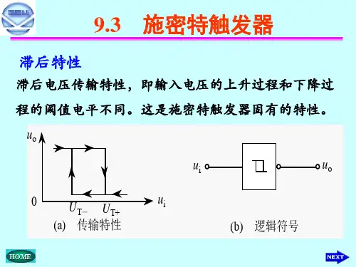
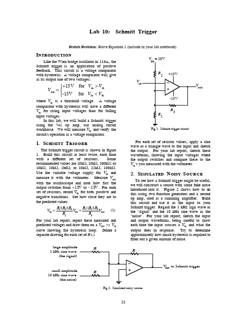
Application BriefUnderstanding Schmitt Triggers Most CMOS, BiCMOS and TTL devices require fastedges on the high and low transitions of their inputs. If the edges are too slow, they can cause excessive current, oscillation, or may damage the device.Slow or Noisy EdgesSlow edges are sometimes hard to avoid at power-up or when using push-button or manual switches with the large capacitors needed for filtering. Heavily loaded outputs can also cause input rise and fall time to be out of specification for the next part down the line. On a normal (non-Schmitt trigger) input, the part will switch at the same point on the rising edge and falling edge. With a slow rising edge the part will switch at the threshold. When the switch occurs, it will require current from Vcc.When current is forced from VCC, the VCC levelcan drop and cause the threshold to shift. When the threshold shifts it will cross the input again causing the part to switch again. This pattern can continue causing oscillation, which can cause excessive current. This pattern can also happen if noise is on the input. The noise can cross the threshold multiple times and cause oscillation or multiple clocking.HysteresisThe solution to these problems is to use a Schmitt trigger device to translate the slow or noisy edges into something faster that will meet the input rise and fall specifications of the following device. A true Schmitt trigger does not have rise and fall time limitations. Parts with Schmitt trigger action have a small amount of hysteresis that helps with noise rejection butstill have an input rise and fall time-limit. Theseparts usually do not have VT specifications in the data sheet and have rise and fall time limitations specified for the inputs in the recommended operating conditions.The true Schmitt trigger input has the switching threshold adjusted where the part will switch at a higher point (Vt+) on the rising edge and at a lower point (Vt–) on the falling edge. The difference in these switching points is called Hysteresis (^Vt). Here is an example of Schmitt trigger specs:SCEA046A – SEPTEMBER 2011 – REVISED NOVEMBER 2022Submit Document FeedbackUnderstanding Schmitt Triggers1It is important to remember (Vt+ max) = Vih and (VT–min) = Vil. In the specs, multiple limits are relatedto the Schmitt trigger inputs. All of the limits areimportant for different reasons. On the input risingedge, the part will switch between (Vt+ min) and (Vt+max). On the falling edge, the part will switch between(Vt– max) and (Vt– min). The part will not switchbetween (Vt– max) and (Vt+ min). This is importantfor noise rejection.The hysteresis is the delta between where the partswitches on the rising edge and where it switches onthe falling edge. The hysteresis will be at least the minand no more than the max (^Vt) spec.Figure 1.In the figure above, the input levels Vih and Vil mustbe greater than (VT+ max) and less than (VT– min)to ensure the part will switch. The switching points onthe above plot are separated to give a clearer visualpicture. In reality, the (VT+ min) and (VT– max) mayoverlap.Input VoltageOne common misconception is that the currentconsumption will be less when switching a slow signalinto a Schmitt trigger. This misconception is partly truebecause the Schmitt trigger prevents oscillation whichcan draw a lot of current; however, the Icc currentmay still be higher due to the amount of time the inputis not at the rail. This is Delta Icc. Delta Icc is wherethe inputs are not at the rails and upper or lower drivetransistors are partially on. The plot below shows Iccacross the input voltage sweep.Figure 2. Supply Current as a Function of InputVoltageSine WavesUse Schmitt triggers to translate a sine wave into asquare wave as shown in this oscillator application.Also, use Schmitt triggers to speed up a slow ornoisy input, or clean up an input, as in the switchde-bouncer circuit.2Understanding Schmitt Triggers SCEA046A – SEPTEMBER 2011 – REVISED NOVEMBER 2022Submit Document FeedbackFigure 3. Oscillator Application Using SchmittTrigger InverterFigure 4. Switch De-bouncer Using SchmittTrigger InverterConclusionSchmitt triggers can be used to change a sine wave into a square wave, clean up noisy signals, andconvert slow edges to fast edges.Figure 5. Sine Wave to Square WaveFigure 6. Clean Noisy SignalsFigure 7. Convert Slow EdgesWe specify the part will switch on the rising edge between (VT+ min) and (VT+ max). We specify the part will switch on the falling edge between (VT– max) and (VT– min).Between (VT+ min) and (VT– max), we specify the part will not switch. This specification can be used for noise rejection. These 2 limits can overlap.We specify a minimum amount of hysteresis as delta VT min.•Vih = (VT+ max)•Vil = (VT– min)Texas Instrument Schmitt trigger functions areavailable in most all technology families from the 30 year old 74XX family to the latest AUP1T family. These two Schmitt-trigger functions are available in most families:•14 for inverting Schmitt trigger•17 for non-inverting Schmitt triggerTexas Instrument also has a complete line of little logic products with Schmitt trigger inputs.ConfigurationsSN74LVC1G57, SN74LVC1G58, SN74LVC1G97, SN74LVC1G98, SN74LVC1G99 SN74AUP1G57, SN74AUP1G58, SN74AUP1G97, SN74AUP1G98, SN74AUP1G99Low to High TranslatorsSN74AUP1T02, SN74AUP1T04, SN74AUP1T08, SN74AUP1T14, SN74AUP1T157, SN74AUP1T158, SN74AUP1T17, SN74AUP1T32, SN74AUP1T86SCEA046A – SEPTEMBER 2011 – REVISED NOVEMBER 2022Submit Document FeedbackUnderstanding Schmitt Triggers 3IMPORTANT NOTICE AND DISCLAIMERTI PROVIDES TECHNICAL AND RELIABILITY DATA (INCLUDING DATA SHEETS), DESIGN RESOURCES (INCLUDING REFERENCE DESIGNS), APPLICATION OR OTHER DESIGN ADVICE, WEB TOOLS, SAFETY INFORMATION, AND OTHER RESOURCES “AS IS” AND WITH ALL FAULTS, AND DISCLAIMS ALL WARRANTIES, EXPRESS AND IMPLIED, INCLUDING WITHOUT LIMITATION ANY IMPLIED WARRANTIES OF MERCHANTABILITY, FITNESS FOR A PARTICULAR PURPOSE OR NON-INFRINGEMENT OF THIRD PARTY INTELLECTUAL PROPERTY RIGHTS.These resources are intended for skilled developers designing with TI products. You are solely responsible for (1) selecting the appropriate TI products for your application, (2) designing, validating and testing your application, and (3) ensuring your application meets applicable standards, and any other safety, security, regulatory or other requirements.These resources are subject to change without notice. TI grants you permission to use these resources only for development of an application that uses the TI products described in the resource. Other reproduction and display of these resources is prohibited. No license is granted to any other TI intellectual property right or to any third party intellectual property right. TI disclaims responsibility for, and you will fully indemnify TI and its representatives against, any claims, damages, costs, losses, and liabilities arising out of your use of these resources.TI’s products are provided subject to TI’s Terms of Sale or other applicable terms available either on or provided in conjunction with such TI products. TI’s provision of these resources does not expand or otherwise alter TI’s applicable warranties or warranty disclaimers for TI products.TI objects to and rejects any additional or different terms you may have proposed.Mailing Address: Texas Instruments, Post Office Box 655303, Dallas, Texas 75265Copyright © 2022, Texas Instruments Incorporated。