FM34018中文
- 格式:pdf
- 大小:317.47 KB
- 文档页数:7

TDA7088T(SC1088)正常工作时的直流特性SC1088(TDA7088T)内部方框图SC1088(TDA7088T)典型接线图使用SC1088(TDA7088T)组装调频接收机●IC产品型号:SC1088(TDA7088T)●产品名称:自动调谐的调频收音机接收电路●产品概述:SC1088是一块适用于单声道便携式或手掌式超小型调频收音机的专用电路,它采用先进的双极型工艺制造,在外围元件的数量、尺寸及成本上变得很重要时,可优先选用该电路。
该电路中含有一个中频(IF)约为70kHz的锁相环回路(FLL),选择性通过一有源RC 滤波器来调整,与中频相应的未调谐信号和低输入信号由静噪电路抑制。
●主要特点:含有单声道收音机从天线接收到音频输出的所有功能静噪功能外接一只变容二极管可进行自动搜寻调谐采用内部AFC电路可进行机械调谐可支持调幅接收应用电源极性反接保护电源电压低至1.8V仍可正常工作●应用:机械调谐方式:可用、也可不用内置的AFC电路自动调谐方式:可实现单方向(向高频方向)的自动搜寻调谐功能;包括复位功能,即回到频段的最低段●封装SC1088——SOP-16-225-1.27●FM自动选台调谐收音机的制作(TDA7088与SC1088引脚及工作原理完全一样,可互换):【功能】本文介绍的袖珍FM电脑选台收音机采用飞利浦公司开发生产的TDA7088T(SC1088)集成块,采用16脚双列扁平封装,工作电压为3V,该电路除包含FM 收音机从天线接收到鉴频输出音频信号的全部功能外,还设有搜索调谐电路、信号检测电路、静噪电路以及压缩中频频偏的频率锁定环FLL电路。
TDA7088T(SC1088)电路的中频频率设计为70kHz,外围电路不用中频变压器,其中频选择由电路内部RC中频滤波器来完成。
该机像数字调谐收音机那样采用电调谐按钮(RUN),另一只是复位按钮(RESET)。
电路接通电源后,按一下搜索按钮,电路自动地由频率低端向高端搜索电台,一旦搜索到电台信号,调谐自动停止。
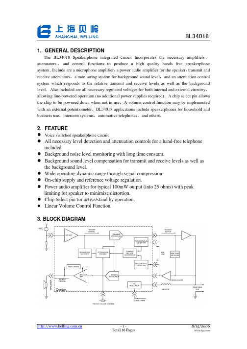
1. GENERAL DESCRIPTIONThe BL34018 Speakerphone integrated circuit Incorporates the necessary amplifiers,attenuators,and control functions to produce a high quality hands free speakerphone system.Include are a microphone amplifier,a power audio amplifier for the speaker,transmit and receive attenuators,a monitoring system for background sound level,and an attenuation control system which responds to the relative transmit and receive levels as well as the background level.Also included are all necessary regulated voltages for both internal and external circuitry,allowing line-powered operation (no additional power supplies required).A chip select pin allows the chip to be powered down when not in use.A volume control function may be implemented with an external potentiometer.BL34018 applications include speakerphones for household and business use,intercom systems,automotive telephones,and others.2. FEATUREVoice switched speakerphone circuit.All necessary level detection and attenuation controls for a hand-free telephone included.Background noise level monitoring with long time constant.Background sound level compensation for transmit and receive levels as well as the background level.Wide operating dynamic range through signal compression.On-chip supply and reference voltage regulation.Power audio amplifier for typical 100mW output (into 25 ohms) with peak limiting for speaker to minimize distortion.Chip Select pin for active/stand by operation.Linear Volume Control Function.3. BLOCK DIAGRAM4. PIN CONFIGURATIONSPin Name Description1 RR A resistor to ground provides a reference current for the transmit and receive attenuators.2 RTX A resistor to ground determines the nominal gain of the transmit attenuator. The transmitchannel gain is inversely proportional to the RTX resistance.3 TXI Input to the transmit attenuator. Input resistance is nominally 5.0 k ohms.4 TXO Output of the transmit attenuator. The TXO output signal drives the input of the transmitlevel detector, as well as the external circuit which drives the telephone line.5 TLI Input of the transmit level detector. An external resistor ac coupled to the TLI pin sets thedetection level. Decreasing this resistor increases the sensitivity to transmit channelsignals.6 TLO Output of the transmit level detector. The external resistor and capacitor set the time thecomparator will hold the system in the transmit mode after speech ceases.7 RLI Input of the receive level detector. An external resistor ac coupled to the RLI pin sets thedetection level. Decreasing this resistor increases the sensitivity to receive channelsignals.8 RLO Output of the receive level detector. The external resistor and capacitor set the time thecomparator will hold the system in the receive mode after speech ceases.9 MCI Microphone amplifier input. Input impedance is nominally 10 k ohms and the dc biasvoltage is approximately equal to VB.10 MCO Microphone amplifier output. The mic amp gain is internally set at 34 dB (50V/V).11 CP1 A parallel resistor and capacitor connected between this pin and VCC holds a voltagecorresponding to the background noise level. The transmit detector compares the CP1voltage with the speech signal from CP2.12 CP2 A capacitor at this pin peak detects the speech signals for comparison with thebackground noise level held at CP1.13 XDI Input to the transmit detector system. The microphone amplifier output is ac coupled tothe XDI pin through an external resistor.14 SKG High current ground pin for the speaker amp output stage. The SKG voltage should bewithin 10 mV of the ground voltage at Pin 22.15 SKO Speaker amplifier output. The SKO pin will source and sink up to 100 mA when accoupled to the speaker. The speaker amp gain is internally set at 34 dB (50V/V).16 V+ Input dc supply voltage. V+ can be powered from Tip and Ring if an ac decouplinginductor is used to prevent loading ac line signals. The required V+ voltage is 6.0 to 11 V(7.5 V nominal) at 7.0 mA.17 AGC A capacitor from this pin to VB stabilizes the speaker amp gain control loop andadditionally controls the attack and decay time of this circuit. The gain control loop limits the speaker amp input to prevent clipping at SKO. The internal resistance at the AGC pin is nominally 110 k ohms.18CS Digital chip select input. When at a logic “0” (<0.7 V) the VCC regulator is enabled. When at a logic “1” (>1.6 V), the chip is in the standby mode drawing 0.5 mA. An openCS pin is a logic “0”. Input impedance is nominally 140 k ohms. The input voltage should not exceed 11 V.19 SKI Input to the speaker amplifier. Input impedance is normally 20 k ohms.20 VCC A 5.4 V regulated output which powers all circuits except the speaker amplifier outputstage. VCC can be used to power external circuitry such as a microprocessor( 3.0 mAmax). A filter capacitor is required. The BL34018 can be powered by a separate regulatedsupply by connecting V+ and VCC to a voltage between 4.5 V and 6.5 V whilemaintaining CS at a logic “1”.21 VB An output voltage equal to approximately VCC/2 which serves as an analog ground forthe speakerphone system. Up to 1.5 mA of external load current may be sourced from VB.Output impedance is 250 ohms. A filter capacitor is required.22Gnd Ground pin for the IC (except the speaker amplifier).23 XDC Transmit detector output. A resistor and capacitor at this pin hold the system in thetransmit mode during pauses between words and phrases. When the XDC pin voltagedecays to ground the attenuators switch from the transmit mode to the idle mode. Theinternal resistor at XDC is nominally 2.6 k ohms.24 VLC Volume control input. Connecting this pin to the slider of a variable resistor providesreceive mode volume control. The VLC pin voltage should be less than or equal to VB. 25 ACF Attenuator control filter. A capacitor connected to this pin reduces noise transients as theattenuator control switches levels of attenuation.26 RXO Output of the receive attenuator. Normally this pin is ac coupled to the input of thespeaker amplifier.27 RXI Input of the receive attenuator. Input impedance is nominally 5.0 k ohms.28 RRX A resistor to ground determines the nominal gain of the receive attenuator. The receivechannel gain is directly proportional to the RRX resistance.5. ELECTRICAL CHARACTERISTICS (Refer to Figure 1)ABSOLUTE MAXIMUM RATINGS(voltages referred to Pin 22) (TA = 25°C)Parameter Value UnitsV+ Terminal Voltage (Pin 16) +12, -1.0 VCS(Pin 18) +12, -1.0 VSpeaker Amp Ground (Pin 14) +3.0, -1.0 VVLC (Pin 24) VCC, -1.0 VStorage Temperature -65 to +150 °C“Maximum Ratings”are those values beyong which the safety of the device cannot be guaranteed, They are not meant to imply that the devices should be operated at these limits. The “Electrical Characteristics” tables provide conditions for actual device operation.Parameter Value UnitsV+ Terminal Voltage (Pin 16) +6.0 to +11 VCS(Pin 18) 0 to +11 VICC (Pin 20) 0 to 3.0 mAVLC (Pin 24) 0.55VB to VB VReceive Signal (Pin 27) 0 to 250 mVrmsMicrophone Signal (Pin 9) 0 to 5.0 mVrmsSpeaker Amp Ground (Pin 14) -10 to +10 mVdcAmbient Temperature -20 to +60 °CELECTRICAL CHARACTERISTICSParameter Symbol Pin Min Typ Max Units SUPPLY VOLTAGESV+ Supply CurrentV+ = 11V, Pin 18 = 0.7VV+ = 11V, Pin 18 = 1.6V IV+ 16--------9.0800mAuAVCC Voltage ( V+ = 7.5V)Line Regulation (6.5V< V+ <11V)VCC∆VCC LN20 4.9--5.4655.9150VdcmVOutput Resistance (ICC = 3.0 mA) Dropout Voltage ( V+ = 5.0 V) ROVCCVCCSAT----6.08020300ohmmVVB Voltage (V+ = 7.5V)Output Resistance ( IB = 1.7 mA)VBROVB21 2.5--2.92503.3--VdcohmATTENUATORSReceive Attenuator Gain (@1.0 kHz)RX Mode, Pin 24 = VB;Pin 27 = 250 mVrmsRange ( RX to TX Modes)Idle Mode, Pin 27 = 250 mVrmsRXO Voltage ( RX Mode)Delta RXO Voltage (Switch from RX to TX Mode)RXO Sink Current (RX Mode)RXO Source Current (RX Mode)RXI Input ImpedanceVolume Control Range ( RX Attenuator Gain, RX Mode, 0.6VB < Pin 24 < VB)GRX∆GRXGRXIVRXO∆VRXOIRXOLIRXOHRRXIVCR26,27 2.040-201.8--751.03.524.56.044-162.3------5.0--1048-123.2100--3.08.032.5dBdBdBVdcmVuAmAkΩdBTransmit Attenuator Gain (@1.0 kHz)TX Mode, Pin 3 = 250 mVrmsRange ( TX to RX Mode)Idle Mode, Pin 3 = 250 mVrmsTXO Voltage ( TX Mode)Delta TXO Voltage (Switch from TX to RX Mode)TXO Sink Current (TX Mode)TXO Source Current (TX Mode)TXI Input ImpedanceGTX∆GTXGTXIVTXO∆VTXOITXOLITXOHRTXI3,44.040-16.51.8--751.03.56.044-132.3------5.08.048-8.53.2100--3.08.0dBdBdBVdcmVuAmAkΩACF Voltage (VCC - Pin 25 Voltage) RX ModeTx ModeIdle Mode ∆VACF 20,25 ------1506.075------mVmVmVSPEAKER AMPLIFIERSpeaker Amp Gain (Pin19 = 20mVrms)SKI Input ImpedanceSKO Voltage ( Pin 19 = Cap Coupled to GND)SKO High Voltage (Pin 19 = 0.1V, -100 mA load at Pin 15)GSPKRSKIVSKOVSKOH15,933152.45.534223.0--35373.6--dBkΩVdcVdcSKO Low Voltage ( Pin 19 = -0.1V, +100 mAload at Pin 15)VSKOL -- -- 600 mV MICROPHONE AMPLIFIERMike Amp Gain (Pin 9 = 10mVrms , 1.0 kHz) Mike Amp Input Resistance GMCIRMCI9,1032.56.534103516dBkΩLOGAMPSRLO Leakage Current (Pin 8 = VB + 1.0V) TLO Leakage Current (Pin 6 = VB + 1.0V) Transmit -Receive Switching Threshold ( Ratio of ITLI to IRLI - at 20 uA - to switch TX-RX Comparator) ILKRLOILKTLOITH865,725----0.8------2.02.01.2uAuATRANSMIT DETECTORXDC Voltage -- Idle Mode-- TX Mode CP2 Current Source VXDCICP22312----5.04.010----13VdcVdcuADISTORTIONRX Mode – RXI to SKO (Pin 27 = 10mVrms ,1.0kHz) TX Mode – MCI to TXO (Pin 9 = 5.0mVrms ,1.0kHz) RXDTXD27,154,9----1.52.0----%%NOTES: 1. V+ = 7.5V, CS= 0.7V except where noted.2. RX Mode : Pin 7 = -100 uA, Pin 5 = +100 uA, except where noted.TX Mode : Pin 5,13 = -100 uA, Pin 7 = +100 uA, Pin 11 = 0V.Idle Mode: Pin 5 = -100 uA, Pin 7, 13 = +100 uA.3. Current into a pin designated as +; current out of a pin designated as - .4. Voltages referred to Pin 22. TA = +25°C.TEMPERATURE CHARACTERISTICS (-20 to 60°C)Parameter Pin TypicalChangeUnits V+ Supply Current (V+ = 11V, Pin 18 = 0.7V) 16 -0.2 %/°C V+ Supply Current (V+ = 11V, Pin 18 = 1.6V) 16 -0.4 %/°C VCC Voltage ( V+ = 7.5V) 20 +0.1 %/°C Attenuator Gain ( Max and Min Settings) ±0.003 dB/°cDelta RXO, TXO Voltages 4,26 ±0.24 %/°C Speaker Amp Gain 15,19 ±0.003 dB/°c Microphone Amp Gain 9,10 ±0.001 dB/°c Microphone Amp Input Resistance 9 +0.4 %/°cTx - Rx Switching Threshold (@ 20 uA) 5,7 ±0.2 nA/°c6. DESIGN GUIDELINES(REF TO FIG. 1)ATTENUATORSThe transmit and receive attenuators are complementary in function, i.e., when one is at maximum gain the other is at maximun attenuation, and vice versa. They are never both on or both off. Their main purpose is to control the transmit and receive paths to provide the half-duplex operation required of a speakerphone. The attenuators are controlled safely by the voltage at the ACF pin. The ACF voltage is provided by the Attenuator Control block, which receives 3 inputs:a) the TX - RX Comparator, b) the Transmit Detector Comparator, and c) the Volume Control. The response of the attenuators is based on the difference of the ACF voltage from VCC (referred to as ∆Vacf). If ∆Vacf is approximately 6mV the transmit attenuator is fully on and the receive attenuator is fully off( transmit mode). If ∆Vacf is approximately 150mV the circuit is in the receive mode. If ∆Vacf is approximately 75mV, the circuit is in the idle mode, and the two attenuators are at gain settings approximately half way (in dB) between their fully on and fully off positions.The maximum gain and attenuation values are determined by the three external resistors RR, RTX, and RRX. RR affects both attenuators according to its value RELATIVE to RTX and RRX. RTX affects the gain and attenuation of only the transmit attenuator, while RRX affects the gain and attenuation of only the receive attenuator. A value of 30 k is recommended for RR as a starting point, and then RTX and RRX selected to suit the particular design goals.The input impedance of the attenuators (at TXI and RXI) is typically 5.0 kΩ, and the maximum input signal which will not cause output distortion is 250 mVrms(707 mVP-P). The 4300 ohm resistor and 0.01 uF capacitor at RXO (in Figure 1) filters out high frequency components in the receive path. This helps minimize high frequency acoustic feedback problems. The filter’s insertion loss is 1.5 dB at 1.0 kHz. The outputs of the attenuators are inverted from their inputs.Referring to the attenuator control block, the ∆Vacf voltage at its output is determined by three inputs. The relationship of the inputs and ouput is summarized in the following truth table:Tx – Rx CompTransmitDet CompVolume Control ∆Vacf ModeTransmit Transmit No Effect 6.0 mV Transmit Transmit Idle No Effect 75 mV Idle Receive Transmit Affects ∆Vacf 50 – 150 mV Receive Receive Idle Affects ∆Vacf 50 – 150 mV ReceiveAs can be seen from the truth table, the Tx-Rx comparator dominates. The Transmit Detector Comparator is effective only in the transmit mode, and the Volume Control is effective only in the receive mode.The Tx-Rx comparator is in the transmit position when there is sufficient transmit signal present over and above any receive signal. The Transmit Detector Comparator then determines whether the transmit signal is a result of background noise ( a relatively stable signal) or speech which consists of bursts. If the signal is due to background noise, the attenuators will be put into the idle mode (∆Vacf = 75 mV). If the signal consists of speech, the attenuators will be switched to the transmit mode (∆Vacf = 6.0 mV.)A further explanation of this function will be found in the section on the transmit detector circuit.The Tx-Rx comparator is in the receive position when there is sufficient receive signal to overcome the background noise AND any speech signals. The ∆Vacf will now be 150 mV IF the volume control is at the maximum position, i.e. VLC (Pin 24) = VB. If VLC is less than VB, the gain of the receive attenuator, and the attenuation of the transmit attenuator, will vary in a complementary manner. At the minimum recommended operating level (VLC = 0.55VB) the gain of the tranmit attenuator is actually greater than that of the receive atttenuator, although it is at receive mode. The effect of varying VLC is to vary ∆Vacf, with a resulting variation in the gains of the attenuators.The capacitor at ACF (Pin 25) smooths the transition between operating modes. This keeps down any “clicks” in the speaker or transmit signal when the ACF voltage switches.The gain separation of the two attenuators can be reduced from the typical 45 dB by adding a resistor between Pins 20(VCC ) and 25(ACF). The effect is a reduction of the maximum ∆Vacf voltage in the receive mode, while not affecting ∆Vacf in the transmit mode.LOGAMPS(Transmit and Receive Level Detectors)The log amps monitor the levels of the transmit and receive signals, so as to tell the Tx-Rx comparator which mode should be in effect. The input signals are applied to the amplifiers (at TLI and RLI) through AC coupling capacitors and current limiting resistors. The value of these components determines the sensitivity of the respective amplifiers, and has an effect on the switching times between tranmit and receive modes. The feedback elements for the amplifiers are back-to-back diodes which provide a logarithmic gain curve. The outputs of the amplifiers are rectified, having a quick rise and a slow decay time. The rise time is determined primarily by the external capacitor and an internal 500 ohm resistor, and is on the order of a fraction of 1 ms. The decay time is determined by the external resistor and capacitor, and is on the order of a fraction of 1 s. The switching time is not fixed, but depends on the relative values of the transmit and receive signals, as well as these external components.The Tx-Rx comparator responds to the voltages at TLO and RLO, which in turn are functions of the currents sourced out of TLI and RLI, respectively. If an offset at the comparator input is desired, e.g., to prevent noise from switching the system, or to give preference to either the transmit or receive channel, this may be achieved by biasing the appropriate input (TLI or RLI). A resistor to ground will cause a DC current to flow out of that input, thus forcing the output of thatamplifier to be biased slightly higher than normal. This amplifier then becomes the preferred one in the system operation. Resistor values from 500 k to 10 M ohms are recommended for this purpose.SPEAKER AMPLIFIERThe speaker amplifier has a fixed gain of 34 dB (50V/V), and is noninverting. The input impedance is nominally 22 kΩ as long as the output signal is below that required to activate the Peak Limiter. Since the output current capability is 100 mA, the output swing is limited to 5.0VPP while load is 25 ohms. The output impedance depends on the output signal level and is relatively low as long as the signal level is not near the maximum limits. At 3 VPP, it is < 0.5 ohms, and at 4.5 VPP, it is < 3 ohms. The output is short circuit protected at approximately 300 mA.When the amplifier is overdriven, the peak limiter causes a portion of the input signal to be shunted to ground, in order to maintain a constant output level. The effect is that of a gain reduction caused by a reduction of the input impedance (at SKI) to a value not less than 2.0 kΩ.The capacitor at Pin 17 (AGC) determines the response time of the peak limiter circuit. When a large input signal is applied to SKI, the voltage at AGC will drop quickly as a current source is applied to the external capacitor. When the large input signal is reduced, the current source is turned off, and an internal 110 kΩ resister discharges the capacitor so the voltage at AGC can return to its normal value (1.9 Vdc). The capacitor additionally stabilizes the peak limiting feedback loop.If there is a need to mute the speaker amplifier without disabling the rest of the circuit, this may be accomplished by connecting a resistor from the AGC pin to ground. A 100 kΩ resister will reduce the gain by 34 dB (0 dB from SKI to SKO), and a 10 kΩ resister will reduce the gain by almost 50 dB.TRANSMIT DETECTOR CIRCUITThe transmit detector circuit, also known as the background noise monitor, distinguishes speech (which consists of bursts) from the background noise ( a relatively constant signal). It does this by storing a voltage level, representative of the average background noise, in the capacitor at CP1( Pin 11). The resistor and capacitor at this pin have a time constant of approximately 5 seconds(in Figure 1). The voltage at Pin 11 is applied to the inverting input of the Transmit Detector Comparator. In the absence of speech signals, the noninverting input receives the same voltage level minus an offset of 36 mV. In this condition, the output of the comparator will be low, the output transistor turned off, and the voltage at XDC (Pin 23) will be at ground. If the Tx-Rx comparator is in the transmit position, the attenuators will be in the idle mode ( ∆Vacf = 75 mV). When speech is presented to the microphone, the signal burst appearing at XDI reaches the noninverting input of the transmit detector comparator before the voltage at the inverting input can change, causing the output to switch high, driving the voltage at XDC up to approximately 4 V. This high level causes the attenuator control block to switch the attenuators from the idle mode to the transmit mode (assuming the Tx-Rx comparator is in the transmit mode).The series resistor and capacitor at XDI (Pin 13) determine the sensitivity of the transmit detector circuit. Increasing the resistor, or lowering the capacitor, will reduce the response at CP2 and CP1.The response at CP2, CP1, XDC to a varying signal at the microphone is as follows:1. CP2 ( Pin 12) follows the peaks of the speech signals, and decays at a rate determined by the10 uA current source and the capacitor at CP2.2. CP1 (Pin 11) increases at a rate determined by the RC at this pin after CP2 has made a positivetransition. It will follow the decay pattern of CP2.3. The noninverting input of the Transmit Detector Comparator follows CP2, gained up by 2.7,and reduced by an offset 36 mV. This voltage, compared to CP1, determines the output of the comparator.4. XDC (Pin 23) will rise quickly to 4 Vdc in response to a positive transition at CP2, but willdecay at a rate determined by the RC at this pin. When XDC is above 3.25 Vdc, the circuit will be in the transmit mode. As it decays towards ground, the attenuators are taken to idle mode. MICROPHONE AMPLIFIERThe microphone amplifier is noninverting, has an internal gain of 34 dB(50 V/V), and a nominal input impedance of 10 kΩ. The output impedance is typically < 15 ohms. The maximum p-p voltage swing available at the output is approximately 2.0 V less than VCC, which is substantially more than what is required in most applications. The input at MCI(Pin 9) should be ac coupled to the microphone so as to not upset the bias voltage. Generally, microphone sensitivity may be adjusted by varying the 2 k microphone bias resistor, rather than by attempting to varying the gain of the amplifier.POWER SUPPLYThe voltage supply at V+ (Pin 16) should be in the range of 6.0 to 11 V, although the circuit will operate down to 4.0 V. The voltage can be supplied either from Tip and Ring, or from a separate supply.It is imperative that the V+ supply be a good ac ground for stability reasons. If it is not well filtered (by a 1000 uF capacitor AT THE IC), any variation at V+ caused by the required speaker current flowing through this pin can cause a low frequency oscillation. The result is usually that the circuit will cut the speaker signal on and off at the rate of a few hertz.VCCVCC (Pin 22) is a regulated output voltage of 5.4 ±0.5 V. Regulation will be maintained as long as V+ is (typically) 80 mV greater than the regulated value of VCC. Up to 3 mA can be sourced from this supply for external use. The output impedance is < 20 ohms. The 47 uF capacitor connecting to this pin is essential for stability reasons. The capacitor must be located adjacent to the IC.If the circuit is deselected, the VCC will go to 0 V. VBVB is a regulated output voltage with a nominal value of 2.9±0.4 V. It is derived from VCC and tracks it, holding a value of approximately 54% of VCC. 1.5 mA can be sourced from this supply at a typically output impedance of 250 ohms. The 47 uF capacitor connecting to this pin is essential for stability reasons. The capacitor must be ocated adjacent to the IC. If the circuit is deselected, the VB will go to 0 V.CHIP SELECTThe CS pin (Pin 18) allows the chip to be powered down anytime its functions are notrequired. A logic “1” level in the range of 1.6 V to 11 V deselects the chip. The input resistance at Pin 18 is > 75 kΩ. The VCC and VB regulated voltages go to 0.0 when the chip is deselected. Leaving Pin 18 open is equivalent to a Logic “0” (chip enabled).SWITCHING TIMEThe switching times of the speakerphone circuit depends not only on the various external components, but also on the operating conditions of the circuit at the time a change is to take effect. For example, the switching time from idle to transmit is generally quicker than the switching time from receive to transmit ( or transmit to receive).The components which most significantly affect the timing between the transmit and receive modes are those at Pins 5 (transmit turn-on), 6 (transmit turn-off), 7 (receive turn-on), and 8 (receive turn-off). These four timing functions are not independent, but interactive since the Tx-Rx comparator operates on a RELATIVE Tx-Rx comparison, rather than on absolute values. The components at Pins 11, 12, 13 and 23 affect the timing from the transmit mode to the idle mode. Timing from the idle mode to transmit mode is relatively quick ( due to the quick charging of the various capacitors), and is not greatly affected by the component values. Pins 5-8 do not affect the idle-to-transmit timing since the Tx-Rx comparator must already be in the transmit mode for this to occur.The following table provides a summary of the effect on the switching time of the various components, including the volume control:Components Tx to Rx Rx to Tx Tx to IdleRC @ Pin 5 Moderate Significant No EffectRC @ Pin 6 Significant Moderate No EffectRC @ Pin 7 Significant Moderate No EffectRC @ Pin 8 Moderate Significant No EffectRC @ Pin 11 No Effect Slight ModerateC @ Pin 12 No Effect Slight SignificantRC @ Pin 13 No Effect Slight SlightRC @ Pin 23 No Effect Slight Significant V@ Pin 24 No Effect Moderate No EffectC@ Pin 25 Moderate Moderate SlightAdditionally, the following should be noted:1) The RCs at Pins 5 and 7 have a dual function in that they affect the sensitivity of the respective logamplifiers, or in other words, how loud the speech must be in order to get control of the speakerphone circuit.2) The RC at Pin 13 also has a dual function in that it determines the sensitivity of the transmit detectorcircuit.3) The volume control affects the switching speed, and the relative response to transmit signals, in thefollowing manner: When the circuit is in the receive mode, reducing the volume control setting increases the signal at TXO, and consequently the signal to the TLI pin. Therefore a given signal at TXI will switch the circuit into the transmit mode quicker at low volume settings.APPLICATIONS INFORMATIONThe BL34018 speakerphone IC is designed to provide the function additionally requiredwhen a speakerphone is added to a standard telephone. The IC provides the necessary relativelevel detection and comparison of the speech signals provided by the talkers at thespeakerphone(near end speaker) and at the distant telephone(far end speaker).The BL34018 is designed for use with an electorate type microphone a 25 ohms speaker, and has an output power capability of 100mW.All external components surrounding this device are passive, however, this IC does require additional circuitry to interface the TIp and Ring telephone lines. Two suggested circuits are shown in the data sheet.Fig 16 depicts a configuration which does not include a handset, dialer, or ringer. The only controls are S1(to make the connection to the line),S2(a "privacy" switch),and the volume control.It is meant to be used in parallel with a normal telephone which has dialing and ringing functions.Fig 17 depicts a means of providing logic level signal that indicate which mode of operationthe BL34018 is in. Comparator A indicates whether the circuit is in receive or transmit mode and comparator B indicates(when in transmit/idle mode) whether the circuit is in the transmit or idle mode. The LM393 dual comparator is chosen because of its low current requirement (<1.0mA),low voltage requirement (as low as 2.0volts), and low cost .。


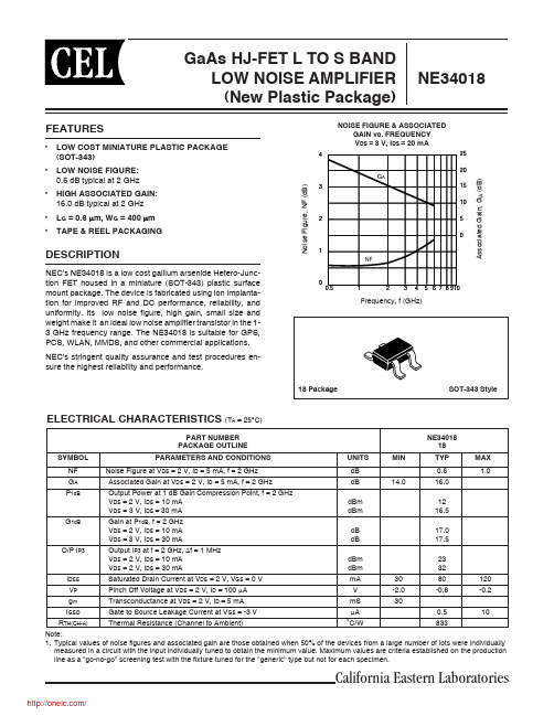
PART NUMBER NE34018PACKAGE OUTLINE18SYMBOL PARAMETERS AND CONDITIONSUNITS MINTYP MAX NF Noise Figure at V DS = 2 V, I D = 5 mA, f = 2 GHz dB 0.6 1.0G A Associated Gain at V DS = 2 V, I D = 5 mA, f = 2 GHz dB 14.016.0P 1dBOutput Power at 1 dB Gain Compression Point, f = 2 GHz V DS = 2 V, I DS = 10 mA dBm 12V DS = 3 V, I DS = 30 mA dBm 16.5G 1dBGain at P 1dB , f = 2 GHz V DS = 2 V, I DS = 10 mA dB 17.0V DS = 3 V, I DS = 30 mAdB 17.5O/P I P3Output I P3 at f = 2 GHz, ∆f = 1 MHz V DS = 2 V, I DS = 10 mA dBm 23V DS = 2 V, I DS = 30 mAdBm 32I DSS Saturated Drain Current at V DS = 2 V, V GS = 0 V mA 3080120V P Pinch Off Voltage at V DS = 2 V, I D = 100 µA V -2.0-0.8-0.2g m Transconductance at V DS = 2 V, I D = 5 mA mS 30I GSO Gate to Source Leakage Current at V GS = -3 V µA 0.510R TH(CH-A)Thermal Resistance (Channel to Ambient)˚C/W833FEATURES•LOW COST MINIATURE PLASTIC PACKAGE (SOT-343)•LOW NOISE FIGURE:0.6 dB typical at 2 GHz •HIGH ASSOCIATED GAIN:16.0 dB typical at 2 GHz •L G = 0.6 µm, W G = 400 µm •TAPE & REEL PACKAGINGNOISE FIGURE & ASSOCIATEDGAIN vs. FREQUENCY V DS = 3 V, I DS = 20 mACalifornia Eastern LaboratoriesELECTRICAL CHARACTERISTICS (T A = 25°C)Note:1.Typical values of noise figures and associated gain are those obtained when 50% of the devices from a large number of lots were individually measured in a circuit with the input individually tuned to obtain the minimum value. Maximum values are criteria established on the production line as a "go-no-go" screening test with the fixture tuned for the "generic" type but not for each specimen.DESCRIPTIONNEC's NE34018 is a low cost gallium arsenide Hetero-Junc-tion FET housed in a miniature (SOT-343) plastic surface mount package. The device is fabricated using ion implanta-tion for improved RF and DC performance, reliability, and uniformity. Its low noise figure, high gain, small size and weight make it an ideal low noise amplifier transistor in the 1-3 GHz frequency range. The NE34018 is suitable for GPS,PCS, WLAN, MMDS, and other commercial applications.NEC's stringent quality assurance and test procedures en-sure the highest reliability and performance.N o i s e F i g u r e , N F (d B )A s s o c i a t e d G a i n , G A (dB )Frequency, f (GHz)G ANF0.5 1 2 3 4 5 6 7 8 91043212520151050FREQ.NF OPT G A ΓOPT(MHz)(dB)(dB)MAG ANGRn/50 V DS = 2 V, I DS = 10 mA900.5620.5.7630.452000.6316.3.6141.282500.6814.1.4951.183000.7013.6.3949.163500.7612.3.2871.124000.8211.6.2080.10 V DS = 2 V, I DS = 30 mA2000.6017.0.5639.232500.7015.3.4346.153000.7614.2.3250.26 V DS = 3 V, I DS = 20 mA900.5620.2.7426 1.542000.6216.8.6242.432500.6614.9.5650.313000.7014.0.4565.243500.8013.2.3676.144000.8412.8.2985.104500.9011.0.2098.08TYPICAL PERFORMANCE CURVES (T A = 25°C)ABSOLUTE MAXIMUM RATINGS 1 (T A = 25°C)SYMBOLSPARAMETERS UNITS RATINGSV DS Drain to Source Voltage V 4V GDO Gate to Drain Voltage V -3V GSO Gate to Source Voltage V -3I DS Drain Current mA I DSS T CH Channel Temperature °C 125T STG Storage Temperature °C -65 to +125P TTotal Power DissipationmW150Note:1.Operation in excess of any one of these parameters may resultin permanent damage.NE34018TYPICAL NOISE PARAMETERS (T A = 25°C)TOTAL POWER DISSIPATIONvs. AMBIENT TEMPERATURET o t a l P o w e r D i s s i p a t i o n , P T (m W )Ambient Temperature, T A (˚C)2001501005050100150200V DS = 2 V, I DS = 5 mAFREQUENCYS 11S 21S 12S 22K MAG 1(GHz)MAG ANG MAGANG MAGANG MAG ANG (dB)0.500.984-15.1 4.945165.00.02080.60.807-7.20.13523.9310.600.979-18.0 4.908162.30.02378.90.803-8.60.15223.2920.700.973-21.0 4.899159.40.02777.00.798-10.00.17422.5870.800.965-23.9 4.871156.70.03175.30.793-11.50.19521.9630.900.958-26.8 4.843153.90.03473.70.788-12.90.21321.5361.000.949-29.8 4.825151.10.03872.10.781-14.40.23121.0371.200.930-35.7 4.783145.60.04568.70.767-17.30.27020.2651.400.906-41.5 4.723140.20.05265.40.751-20.20.31419.5821.600.881-47.5 4.660134.70.05862.20.734-23.10.35419.0501.800.853-53.6 4.605129.30.06459.10.715-26.00.39518.5702.000.821-59.8 4.531123.80.07056.00.696-28.90.43818.1112.500.737-76.3 4.332110.50.08248.20.648-36.00.54217.2293.000.648-94.2 4.09297.60.09241.40.600-42.40.64316.4813.500.569-113.6 3.80585.30.09835.30.556-47.70.74815.8914.000.512-133.0 3.51673.90.10230.50.518-51.80.84515.3744.500.482-150.9 3.24863.80.10527.20.480-54.90.93214.9045.000.472-165.2 3.02554.70.10825.30.444-57.8 1.00414.0745.500.468-175.7 2.84646.40.11224.50.405-61.0 1.06812.4596.000.464176.0 2.71438.40.11823.70.367-65.4 1.10711.6226.500.456167.9 2.60130.50.12622.40.331-71.6 1.13010.9557.000.441158.2 2.50522.10.13420.20.302-80.8 1.14910.3727.500.422144.3 2.41713.30.14218.00.283-92.2 1.1619.8748.000.411127.52.3214.00.15115.00.281-105.91.1529.503TYPICAL SCATTERING PARAMETERS (T A = 25°C)NE34018MAG = Maximum Available GainMSG = Maximum Stable GainNote:1.Gain Calculations:MAG =|S 21||S 12|K - 1 ).2(K ±∆ = S 11 S 22 - S 21 S 12When K ≤ 1, MAG is undefined and MSG values are used.MSG =|S 21||S 12|, K = 1 + | ∆ | - |S 11| - |S 22|2222 |S 12 S 21|,NE34018TYPICAL SCATTERING PARAMETERS (T A = 25°C)FREQUENCYS 11S 21S 12S 22K MAG 1(GHz)MAG ANG MAG ANG MAG ANG MAGANG (dB) 0.500.978-17.0 6.806162.80.01880.10.723-7.50.17825.7760.600.969-20.3 6.731159.70.02278.70.719-9.10.20024.8570.700.960-23.6 6.691156.50.02577.30.712-10.50.22424.2760.800.949-26.9 6.624153.40.02875.50.706-12.00.25323.7400.900.938-30.1 6.559150.30.03273.60.698-13.40.28123.1171.000.924-33.3 6.502147.20.03572.40.690-14.90.30722.6901.200.897-39.8 6.371141.20.04169.20.673-17.80.35621.9141.400.865-46.0 6.217135.30.04766.30.655-20.60.41021.2151.600.831-52.4 6.065129.50.05363.40.635-23.40.46020.5861.800.796-58.7 5.912123.90.05860.70.614-26.10.50920.0832.000.757-65.1 5.750118.30.06358.10.594-28.80.56019.6032.500.658-81.95.336105.00.07451.70.546-35.30.67718.5803.000.563-100.1 4.90992.40.08346.50.501-41.20.78217.7193.500.483-119.7 4.47880.80.09141.80.463-45.90.87316.9204.000.432-139.4 4.08070.20.09738.10.429-49.50.95216.2394.500.409-157.23.73360.80.10335.10.388-53.3 1.01814.7715.000.406-171.0 3.44852.30.10933.20.363-53.8 1.05713.5385.500.408179.2 3.22344.50.11731.60.327-55.6 1.08512.6186.000.411171.4 3.05037.00.12629.90.293-58.3 1.09711.9396.500.408163.8 2.90629.40.13627.50.259-62.8 1.10611.3207.000.397154.5 2.78221.50.14524.10.232-71.3 1.11710.7527.500.383140.6 2.67213.20.15620.80.211-83.2 1.11210.2988.000.376123.62.5604.40.16616.50.204-99.51.1049.917V DS = 2 V, I DS = 10 mAMAG = Maximum Available GainMSG = Maximum Stable GainNote:1.Gain Calculations:MAG =|S 21||S 12|K - 1 ).2(K ±∆ = S 11 S 22 - S 21 S 12When K ≤ 1, MAG is undefined and MSG values are used.MSG =|S 21||S 12|, K = 1 + | ∆ | - |S 11| - |S 22|2222 |S 12 S 21|,FREQUENCYS 11S 21S 12S 22K MAG 1(GHz)MAG ANG MAG ANG MAG ANG MAGANG (dB)0.500.969-18.68.533160.80.01781.20.635-7.30.22127.0070.600.958-22.18.416157.30.02079.40.631-8.80.25626.2410.700.946-25.78.331153.80.02377.80.624-10.20.28925.5900.800.931-29.28.211150.40.02676.40.617-11.60.32424.9940.900.916-32.78.092147.10.02975.10.610-12.90.35424.4571.000.899-36.17.982143.70.03273.80.601-14.30.38723.9701.200.864-42.97.737137.30.03771.10.584-16.90.45123.2041.400.825-49.37.469131.10.04368.50.566-19.40.51222.3981.600.785-55.87.205125.20.04866.10.547-21.80.57021.7641.800.745-62.1 6.948119.50.05363.80.527-24.20.62321.1762.000.701-68.6 6.692113.90.05861.70.509-26.50.67520.6212.500.596-85.3 6.075100.90.06956.6 0.467-32.40.78619.4473.000.499-103.3 5.49588.90.07952.00.428-37.80.87918.4233.500.422-123.1 4.95377.80.08847.90.397-42.40.95217.5044.000.374-142.9 4.47767.80.09644.30.369-45.8 1.00916.1184.500.357-160.6 4.07358.90.10441.10.340-47.7 1.04714.5965.000.359-174.1 3.74550.90.11238.60.310-48.8 1.07313.5895.500.366176.6 3.48743.40.12236.20.278-49.1 1.08412.7966.000.372169.3 3.28536.20.13333.60.248-50.0 1.08412.1606.500.372162.1 3.11829.00.14430.40.219-52.7 1.08611.5717.000.365153.0 2.97521.40.15426.40.193-60.2 1.09011.0317.500.353139.1 2.85213.40.16522.20.169-72.2 1.08810.5698.000.348122.02.7295.00.17617.40.156-91.31.07910.189V DS = 2 V, I DS = 20 mAMAG = Maximum Available GainMSG = Maximum Stable GainNote:1.Gain Calculations:MAG =|S 21||S 12|K - 1 ).2(K ±∆ = S 11 S 22 - S 21 S 12When K ≤ 1, MAG is undefined and MSG values are used.MSG =|S 21||S 12|, K = 1 + | ∆ | - |S 11| - |S 22|2222 |S 12 S 21|,NE34018TYPICAL SCATTERING PARAMETERS (T A = 25°C)TYPICAL SCATTERING PARAMETERS (T A = 25 °C)NE34018FREQUENCYS 11S 21S 12S 22K MAG 1(GHz)MAG ANG MAG ANG MAG ANG MAGANG (dB)0.500.977-17.0 6.912162.90.01880.50.744-7.50.17025.8430.600.969-20.2 6.836159.70.02179.00.740-9.00.19425.1260.700.959-23.5 6.795156.50.02477.10.733-10.40.22624.5200.800.948-26.8 6.728153.40.02775.40.727-11.90.25223.9650.900.937-30.0 6.659150.30.03173.70.719-13.30.27823.3201.000.923-33.2 6.602147.20.03472.40.712-14.80.30222.8821.200.895-39.6 6.467141.20.04069.10.695-17.60.35522.0861.400.863-45.8 6.310135.30.04566.20.676-20.30.41021.4681.600.829-52.1 6.152129.50.05163.50.656-23.00.45920.8141.800.793-58.4 5.996123.90.05660.80.636-25.70.50820.2972.000.754-64.8 5.830118.30.06158.00.616-28.30.55919.8032.500.656-81.4 5.407105.10.07152.10.568-34.60.67418.8173.000.559-99.2 4.97392.70.08046.70.524-40.10.78117.9353.500.479-118.5 4.53881.10.08742.30.486-44.70.87617.1734.000.426-138.0 4.13870.60.09338.90.454-48.20.95316.4834.500.402-155.8 3.78861.20.09936.40.422-50.6 1.01115.1735.000.397-169.6 3.50052.80.10534.60.389-52.6 1.05813.7575.500.399-179.6 3.27445.00.11233.30.355-54.6 1.09012.8336.000.401172.6 3.10137.60.12131.80.322-57.5 1.10012.1636.500.399165.2 2.95630.10.13129.60.290-62.2 1.10411.5737.000.389156.1 2.83222.30.14026.60.264-70.4 1.11211.0267.500.387144.7 2.79815.40.15320.40.245-81.6 1.06311.0858.000.365125.82.6145.40.16119.30.240-96.51.09410.240V DS = 3 V, I DS = 10 mAMAG = Maximum Available GainMSG = Maximum Stable GainNote:1.Gain Calculations:MAG =|S 21||S 12|K - 1 ).2(K ±∆ = S 11 S 22 - S 21 S 12When K ≤ 1, MAG is undefined and MSG values are used.MSG =|S 21||S 12|, K = 1 + | ∆ | - |S 11| - |S 22|2222 |S 12 S 21|,00.5000.969-18.78.662160.80.01681.10.667-7.30.21527.3350.6000.957-22.28.541157.30.01979.10.663-8.80.25526.5280.7000.945-25.88.454153.70.02278.00.655-10.20.28225.8460.8000.930-29.38.332150.30.02576.30.649-11.60.31825.2280.9000.915-32.78.209147.00.02874.80.641-12.90.35024.6711.0000.898-36.18.096143.60.03173.30.632-14.30.38424.1691.2000.862-42.87.844137.20.03670.60.615-16.90.44723.3821.4000.823-49.37.571131.10.04168.10.596-19.30.50922.6641.6000.781-55.77.299125.10.04665.70.577-21.70.56922.0051.8000.741-62.07.036119.40.05163.50.557-24.00.62121.3982.0000.697-68.4 6.775113.90.05661.40.539-26.40.67020.8272.2500.644-76.6 6.458107.20.06158.70.517-29.30.73120.2482.5000.591-84.9 6.144100.90.06656.50.496-32.00.78619.6892.7500.541-93.7 5.84894.80.07154.30.476-34.70.83319.1573.0000.493-102.7 5.55388.90.07552.10.458-37.10.88418.6953.5000.415-122.2 5.00778.00.08448.20.426-41.50.95617.7534.0000.368-141.9 4.52668.00.09144.90.399-44.7 1.01616.1884.5000.349-159.7 4.11959.20.09942.20.372-46.8 1.05214.7985.0000.349-173.2 3.79051.20.10739.90.343-48.1 1.07713.7945.5000.357177.4 3.53243.80.11637.90.313-49.1 1.08913.0216.0000.362170.2 3.33236.70.12735.60.284-50.8 1.08612.4056.5000.363163.3 3.16629.50.13832.70.255-54.2 1.08411.8367.0000.356154.4 3.02422.00.14828.80.230-61.8 1.08711.3077.5000.343140.7 2.90214.10.16025.00.208-73.1 1.07910.8768.0000.336123.72.7825.70.17120.30.199-89.61.06710.531V DS = 3 V, I DS = 20 mAFREQUENCYS 11S 21S 12S 22K MAG 1(GHz)MAG ANG MAG ANG MAG ANG MAG ANG (dB)MAG = Maximum Available GainMSG = Maximum Stable GainNote:1.Gain Calculations:MAG =|S 21||S 12|K - 1 ).2(K ±∆ = S 11 S 22 - S 21 S 12When K ≤ 1, MAG is undefined and MSG values are used.MSG =|S 21||S 12|, K = 1 + | ∆ | - |S 11| - |S 22|2222 |S 12 S 21|,NE34018TYPICAL SCATTERING PARAMETERS (T A = 25 °C)ParametersQ1 ParametersQ1VTO -0.6885RG 4VTOSC 0RD 1.5ALPHA 5RS 2BETA0.1838RGMET 0GAMMA 0.038KF 0GAMMADC0.03AF 1Q 1.8TNOM 27DELTA 0.25XTI 3VBI 0.7EG 1.43IS 3e-13VTOTC 0N 1BETATCE 0RIS 0FFE1RID 0TAU 4e-12CDS 0.1e-12RDB 5000CBS 1e-11 CGSO 0.95e-12CGDO 0.04e-12DELTA10.3DELTA20.05FC 0.5VBRInfinityParameter Units time seconds capacitance farads inductance henries resistance ohms voltage volts currentampsFET NONLINEAR MODEL PARAMETERS (1)UNITSMODEL RANGEFrequency:0.5 to 6 GHz Bias:V DS = 1 V to 3 V, I D = 5 mA to 40 mA Date:6/97(1) Series IV Libra TOM ModelNE34018NE34018 NONLINEAR MODELSCHEMATICGA TEDRAINNE34018PACKAGE OUTLINE 18OUTLINE DIMENSIONS (Units in mm)PART NUMBERQTY IDSS RANGEMARKING (mA)NE34018-ABulk up to 3 K 30-120V63 or V64NE34018-TI-63-A 3 K/Reel 30-65V63 NE34018-TI-64-A3 K/Reel60-120V64ORDERING INFORMATIONEXCLUSIVE NORTH AMERICAN AGENT FOR RF, MICROWAVE & OPTOELECTRONIC SEMICONDUCTORS• Headquarters • 4590 Patrick Henry Drive • Santa Clara, CA 95054-1817 • (408) 988-3500 • Telex 34-6393 • FAX (408) 988-0279DATA SUBJECT TO CHANGE WITHOUT NOTICELife Support ApplicationsThese NEC products are not intended for use in life support devices, appliances, or systems where the malfunction of these products can reasonably be expected to result in personal injury. The customers of CEL using or selling these products for use in such applications do so at their own risk and agree to fully indemnify CEL for all damages resulting from such improper use or sale.1-1064590 Patrick Henry Drive Santa Clara, CA 95054-1817Telephone: (408)919-2500Facsimile:(408) 988-0279Subject:Compliance with EU DirectivesCEL certifies, to its knowledge, that semiconductor and laser products detailed below are compliant with the requirements of European Union (EU) Directive 2002/95/EC Restriction on Use of Hazardous Substances in electrical and electronic equipment (RoHS) and the requirements of EU Directive 2003/11/EC Restriction on Penta and Octa BDE.CEL Pb-free products have the same base part number with a suffix added. The suffix –A indicates that the device is Pb-free. The –AZ suffix is used to designate devices containing Pb which areexempted from the requirement of RoHS directive (*). In all cases the devices have Pb-free terminals. All devices with these suffixes meet the requirements of the RoHS directive.This status is based on CEL’s understanding of the EU Directives and knowledge of the materials that go into its products as of the date of disclosure of this information.Restricted Substanceper RoHS Concentration Limit per RoHS (values are not yet fixed)Concentration containedin CEL devices -A-AZ Lead (Pb)< 1000 PPM Not Detected(*)Mercury < 1000 PPM Not Detected Cadmium< 100 PPM Not Detected Hexavalent Chromium < 1000 PPM Not Detected PBB < 1000 PPM Not Detected PBDE< 1000 PPMNot DetectedIf you should have any additional questions regarding our devices and compliance to environmental standards, please do not hesitate to contact your local representative.Important Information and Disclaimer: Information provided by CEL on its website or in other communications concerting the substancecontent of its products represents knowledge and belief as of the date that it is provided. CEL bases its knowledge and belief on information provided by third parties and makes no representation or warranty as to the accuracy of such information. Efforts are underway to better integrate information from third parties. CEL has taken and continues to take reasonable steps to provide representative and accurate information but may not have conducted destructive testing or chemical analysis on incoming materials and chemicals. CEL and CEL suppliers consider certain information to be proprietary,and thus CAS numbers and other limited information may not be available for release.In no event shall CEL’s liability arising out of such information exceed the total purchase price of the CEL part(s) at issue sold by CEL to customer on an annual basis.See CEL Terms and Conditions for additional clarification of warranties and liability.分销商库存信息:CELNE34018-64-A NE34018-A NE34018-T1-64-A NE34018-EVGA19。
电台全部频率表0.5-1.8M 广播频段MF(AM) 525KHz-1605KHz 9KHz 中波调幅广播北京电台首都生活广播603中央电台中国之声639中央电台经济之声720中央电台文艺之声(第9套) 747北京电台新闻频道828/846国际电台HIT-FM 900北京电台体育频道927国际电台ROUND THE CLOCK 846/1008中央电台朝鲜语广播1206北京电台经济频道1026国际电台英语频道12511.8-30M 短波波段2182kHz 为无线的国际遇险频率4125 kHz频率用作2182 kHz频率的补充HF(SW) 3.5-29.7MHz 9KHz 短波调幅广播及单边带通讯玩具遥控器通信设备带宽(KHz)发射功率(mW)频率(MHz) 遥控设备带宽(KHz) 发射功率(W) 频率(MHz)1 <12 ≤100 26.965 1 ≤8 ≤1 26.9752 <12 ≤100 26.985 2 ≤8 ≤1 26.9953 <12 ≤100 27.005 3 ≤8 ≤1 27.0154 <12 ≤100 27.025 4 ≤8 ≤1 27.0455 <12 ≤100 27.055 5 ≤8 ≤1 27.0656 <12 ≤100 27.075 6 ≤8 ≤1 27.0957 <12 ≤100 27.105 7 ≤8 ≤1 27.1158 <12 ≤100 27.125 8 ≤8 ≤1 27.1459 <12 ≤100 27.165 9 ≤8 ≤1 27.19510 <12 ≤100 27.185 10 ≤8 ≤30-76〔59〕M 50M业余波段无绳使用频率划分表一座机频率(MHz) 发射频率(MHz)1 48.000 74.0002 48.025 74.0253 48.050 74.0504 48.075 74.0755 48.100 74.1006 48.125 74.1257 48.150 74.1508 48.175 74.1759 48.200 74.20010 48.225 74.22511 48.250 74.25012 48.275 74.27513 48.300 74.30014 48.325 74.32515 48.350 74.35016 1.665 48.37517 1.690 48.40018 1.715 48.42519 1.690 48.45020 1.740 48.475无绳使用频率划分表二座机发射(MHz) 发射(MHz)1 45.000 48.0002 45.025 48.0253 45.050 48.0504 45.075 48.0755 45.100 48.1006 45.125 48.1257 45.150 48.1508 45.175 48.1759 45.200 48.20010 45.225 48.225VHF 48.5-92MHz 8MHz 电视及数据广播中国电视频道频率划分表(单位:MHz)频道号/频率范围图像载频伴音载频VHF-L (Ⅰ)DS-1 48.5~56.5 49.75 56.25DS-2 56.5~64.5 57.75 64.25DS-3 64.5~72.5 65.75 72.25DS-4 76.0~84.0 77.25 83.75DS-5 84.0~92.0 85.25 91.7564.5-72.5M 〔广播为主〕76〔59〕-108M 调频广播VHF(FM) 88-108MHz 150KHz 调频广播及数据广播北京87.6 北京人民广播电台文艺台北京88.2 中国国际广播电台EasyFM北京88.7 中国国际广播电台北京90.0 中央人民广播电台第三套节目文艺调频北京91.5 中国国际广播电台EasyFM北京96.6 中央人民广播电台第二套节目经济频道北京97.4 北京人民广播电台音乐台北京99.6 中央人民广播电台第二套节目北京101.8 中央人民广播电台第四套节目民族广播北京103.9 北京人民广播电台交通台北京106.1 中央人民广播电台第一套节目综合频道108-137M 航空波段121.5MHz频率用于遇险和紧急时的无线134.200 北京空管北京地区航空频率表及收听教程1276:ATIS1181:TOWER 塔台1216:DELIVERY 放行1217:GROUND CONTROL 地面管制1190:ARRIVAL 进场1185:APPROUCH 进近1197:DEPATURE 离场1256:BEIJING CONTROL 北京区调1283:RAIDER 北京雷达1232:DA LIAN CONTROL 大连区调1132,1134 类似区调中文名称英文名称呼号区调Area control centre Beijing Control近进Approach control Beijing Aproach离场Approach control radar arrival Beijing Arrival进场Approach control radar departures Beijing Departure塔台Aerodrome control Beijing Tower地面Surface movement control Beijing Ground放行Clearance delivery Beijing Delivery精密近进雷达Precision approach radar Beijing Precision机坪Apron control Beijing Apron签派Company dispatch Air China Dispatch航空术语注解:via:经过squawk:应答机编码。
HX3208型FM 微型贴片收音机(SMT 实习)姓 名学 号 *****XXX院、系、部电气工程系 班 号完成时间 2013年1月 5 日※※※※※※※※※ ※※※※※※※※※※※※ 2013 电子电路课程设计目录第一章 SMT简介······················错误!未定义书签。
第二章实习要求······················错误!未定义书签。
第三章设计要求······················错误!未定义书签。
第四章实验内容······················错误!未定义书签。
第五章实验前的检查与准备··················错误!未定义书签。
UTC MC34018 LINEAR INTEGRATED CIRCUITUTC UNISONIC TECHNOLOGIES CO., LTD.1QW-R108-006,AVOICE SWITCHEDSPEAKER-PHONE CIRCUITDESCRIPTIONThe UTC MC34018 speaker-phone integrated circuit incorporates the necessary functions to produce a high quality hands-free speaker-phone system. The applications include household and office speaker-phones, intercom systems, hand free kit for mobile phones, and others.FEATURES*All necessary level detection and attenuation controls for a hand-free telephone included.*Background noise level monitoring with long time constant.*Background sound level compensation for transmit and receive levels as well as the background level.*Wide operating dynamic range through signal compression.*On-chip voltage regulators illuminate external regulators for lining operation.*Power audio amplifier for typical 100mW output (into 25 ohms)with peak limiting for speaker to minimize distortion.*Chip Select pin for active/stand by operation.*Volume control function for external volume control. *Standard 28-pin plastic DIP and SOP package.UTC MC34018 LINEAR INTEGRATED CIRCUIT BLOCK DIAGRAMRECEIVE VOLUME CONTROLPIN CONFIGURATIONSPIN NAME DESCRIPTION1 RR A resistor to ground provides a reference current for the transmit and receive attenuators2 RTX A resistor to ground determines the nominal gain of the transmit attenuator ,the transmit channel gainis inversely proportional to RTX resistance.3 TXI Input to the transmit attenuator. Input resistance is nominally 5.0k ohms.4 TXO Output of the transmit attenuator. The TXO output signal drivers the input of transmit level detcetor,as well as the external circuit which drivers the telephone line.5 TLI Input of the transmit level detector. An external resistor ac coupled to The TLI pin sets the detectionlevel. Decreasing this resistor increases the sensitivity to transmit channel signals.6 TLO Output of the transmit level detector. The external resistor and capacitor set the time the comparatorwill hold the system in the transmit mode after speech ceases.7 RLI Input of the receive level detector. An external resistor ac coupled to The RLI pin sets the detectionlevel. Decreasing this resistor increases the sensitivity to receive channel signals.8 RLO Output of the receive level detector. The external resistor and capacitor set the time the comparatorwill hold the system in the receive mode after speech ceases.9 MCI Microphone amplifier input. Input impedance is nominally 10k ohms and the dc bias voltage isapproximately equal to VB10 MCO Microphone amplifier output. The MIC amp gain is internally set at 34dB(50V/V).11 CP1 A parallel resistor and capacitor connected between this pin and VCC holds a voltage correspondingto the background noise level. The transmit detector compares the CP1 voltage with the speechsignal from CP2.12 CP2 A capacitor at this pin peak detects the speech signals for comparison with the background noiselevel held at CP1.13 XDI Input to the transmit detector system. The microphone amplifier output is ac coupled to the XDI pinthrough an external resistor.UTC UNISONIC TECHNOLOGIES CO., LTD. 2QW-R108-006,AUTC MC34018 LINEAR INTEGRATED CIRCUITUTC UNISONIC TECHNOLOGIES CO., LTD.3QW-R108-006,AELECTRICAL CHARACTERISTICS (referred to fig. 1)PARAMETER SYMBOL MIN TYP MAX UNITSUPPLY VOLTAGESV+ Supply Current V+=11V,Pin 18=0.7V V+=11V,Pin 18=1.6V I V+9.0 800 mA µA VCC Voltage(V+=7.5V) LineRegulation(6.5V<V+<11V) Output Resistance(I CC =3mA) Dropout Voltage(V+=5.0V) Vcc ∆Vcc LN Ro Vcc Vccsat 4.95.4 656.0 80 5.9 150 20 300 Vdc mV ohms mV VB Voltage(V+=7.5V) Output Resistance(I B =1.7mA)Vb Rovb2.52.9 2503.3Vdc ohmsUTC MC34018 LINEAR INTEGRATED CIRCUITUTC UNISONIC TECHNOLOGIES CO., LTD.4QW-R108-006,A(continued)PARAMETER SYMBOL MIN TYP MAX UNITATTENUATORSReceive Attenuator Gain(1.0kHz) Rx Mode, Pin 24= VB, Pin 27 = 250Mvrms Range (Rx to Tx Modes) Idle Mode, Pin 27= 250mVrms G RX ∆G RX G RI 2.0 40 -20 6.0 44 -16 10 48 -12 dBdB dBRXO Voltage (Rx Mode) V RXO 1.8 2.3 3.2 mVDelta RXO Voltage (Switch from Rx to Tx Mode)∆V RXO 100 mVRXO Sink Current (Rx mode) I RXOL 75µA RXO Source Current (Rx mode) I ROXH 1.0 3.0 mA RXI Input Resistance R RXI 3.5 5.0 8.0 k ΩVolume Control Range (Rx Attenuator Gain, Rx Mode, 0.6VB<Pin 24<VBV CR24.5 32.5 dB ATTENUATORSTransmit Attenuator Gain (1.0kHz) Tx Mode, Pin 3 = 250mVrms Range, (Tx to Rx Mode) Idle Mode, Pin 3 = 250Mvrms G TX ∆G TX G TXI 4.0 40 -16.5 6.0 44 -13 8.0 48 -8.5 dBdB dBTXO Voltage (Tx mode) V TXO 1.8 2.3 3.2 VdcDelta TXO Voltage (switch from Tc to Rx Mode)∆V TXO 100 mVTXO Sink Current (Tx mode) I TXOL 75µA TXO Source Current (Tx mode) I TXOH 1.0 3.0 mA TXO Input Resistance R TXI 3.5 5.0 8.0 k ΩACF Voltage (VCC-Pin 25 Voltage) Rx Mode Tx Mode Idle Mode ∆V ACF 150 6.0 75mV mVmVSPEAKER AMPLIFIER Speaker Amp Gain (pin 19 = 20mVrms)G SPK 33 34 35 dB SKI Input Resistance R SKI 15 22 37 k Ω SKO Voltage ( Pin 19 =Cap couple to GND)V SKO 2.4 3.0 3.6 Vdc SKO High Voltage ( Pin 19 = 0.1V, -100mA Load at Pin 15)V SKOH 5.5 Vdc SKO Low Voltage (pin 19=0.1V, +100mA Load at Pin 15) V SKOL 600 mV MICROPHONE AMPLIFIER Microphone Amp Gain ( Pin 9 = 10mVrms,1KHz) G MCI 32.5 34 35 dB Microphone Amp Input Resistance R MCI 6.5 10 16 k ΩUTC MC34018 LINEAR INTEGRATED CIRCUITUTC UNISONIC TECHNOLOGIES CO., LTD.5QW-R108-006,ANote 2:Rx mode:pin7=-100µA,pin5=+100µA, except where noted. Tx mode: pin 5,13=-100µA, pin 7=+100µA, pin 11=0V. Idle mode: Pin 5=-100µA, pin 7,13=+100µA.Note 3:Current into a pin designed as +,current out of a pin designed -; Note 4:Voltage referred to pin 22,Tamb=25°C.TEMPERATURE CHARACTERISTICS (-20 TO +60°C )PARAMETER PIN TYP CHANGE UNITV+ Supply Current ( V+ 11V,Pin 18 = 0.7V )16 -0.2 %/°C V+ Supply Current(V+ 11V,Pin 18 = 1.6V ) 16 -0.4 %/°C VCC Voltage( V+ = 7.5V )20 +0.1 %/°C Attenuator Gain ( Max and Min Setting ) +-0.003 dB/°C Delta RXO,TXO Voltage 4,26 +-0.24 %/°C Speaker AMP Gain 15,19 +-0.001 dB/°C Microphone AMP Gain9,10 +-0.4 dB/°C Microphone Amp Input Resistance 9 +0.4%/°C Tx-Rx Switching Threshold (20µA) 5,7 +-0.2nA/°CDESIGN GUIDELINES (REF TO FIG. 1)ATTENUATORSThe transmit and receive attenutors are complementary in function, i.e., when one is at maximum gain the other is at maximum attenuator, and vice versa. They are never both on or both off. Their main purpose is to control the transmit and receive paths to provide the half-duplx operation required of a speaker-phone. The attenuators are controlled solely by the voltage at the ACF pin(pin 25).The ACF voltage is provided by the attenuator control block,UTC MC34018 LINEAR INTEGRATED CIRCUITUTC UNISONIC TECHNOLOGIES CO., LTD.6QW-R108-006,Awhich receives 3 inputs: a) the Rx-Tx comparator, b) the transmit detector comparator, and c)the volume control. The response of the attenuators is based on the difference of the ACF voltage from VCC, and therefore a simple method for monitoring the circuit operation is to monitor this voltage difference(referred to as ∆Vacf).If ∆Vacf is approximately 150 millivolts the circuit is in the receive mode. If ∆Vacf is approximately 75 millivolts the circuit is in the idle mode, and two attenuators are at gain setting approximately half way(in dB) between their fully on and fully off positions.The maximum gain and attenuation values are determined by the three resistors RR,RTX,RRX(referred to Fig2,3,4).RR affects both attenuators according to its value RELATIVE to RTX and RRX, which is why Fig 4 indicates the variations versus the ratio of the other resistors to RR.(GRX and GTX are the maximum gains, and ARX and ATX are maximum attenuations).RTX affects the gain and attentuator according to Fig 3.As can be seen from the figures, the gain difference(from on to off) is a reasonably constant 45dB until the upper gain limit is approached. A value of 30K is recommended for RR as a starting point, and then RTX and RRX selected to suit the particular design goals.The input impedance of the attenuators (at TXI and RXI) is typically 5.0k ohms, and the maximum input signal which will not cause output distortion is 250mVrms(707mVp-p).The 4300 ohms resistor and 0.01µCapacitor at RXO(in fig 1)filters out high frequency components in the receive path. This helps minimize high frequency acoustic feedback problems which may occur if the filter were not present. The filter's insertion loss is a 1.5dB at 1.0kHz.The outputs of the attenuators are inverted from their inputs.Referring to the attenuator control block, the ∆Vacf voltage at its output is determined by three inputs. The relationship of the inputs and outputs is summarized in the following truth table.TX-RX COMPTRANSMIT DETCOMP VOLUME CONTROL∆VACF MODETransmit Transmit No Effect 6.0mV Transmit Transmit Idle No Effect 75mV IdleReceive Transmit Affects ∆Vacf 50-150mV Receive Receive Idle Affects ∆Vacf 50-50mV ReceiveAs can be seen from the truth table, the Tx-Rx comparator dominates. The transmit detector comparator is effective only in the receive mode.The Tx-Rx comparator is in the transmit position when there is sufficient transmit signal present over and above any receive signal. The transmit detector comparator then determined whether the transmit signal is a result of background noise(1 relatively stable signal),or speech which consists of bursts.If the signal is due to background noise, the attenuators will be put into the idle mode(∆Vacf=75mV).If the signal consists of speech, the attenuator will be switched to the transmit mode(∆Vacf=6.0mV).A further explanation of this function will be found in the section on the transmit detector circuit.The Rx-Tx Comparator is in the receive position when there is sufficient receive signal to overcome the background noise AND any speech signals. The ∆Vacf voltage will now be 150mV IF the volume control is at the maximum position, i.e. VLC(pin 24)=VB. If VLC is less than Vb, the gain of the receive attenuator, will vary in a complementary manner as shown in fig 5.It can be seen that at the minimum recommended operating level(VLC=0.55VB) the gain of the transmit atternuator is actually greater than that of the receive attenuator. The effect of varying VLC is to vary ∆Vacf, with a resulting variation in the gains of the attenuators, Fig 6 shows the gain variation with ∆Vacf.The capacitor at ACF(pin 25) smoothes the transition between operating modes. This keeps down any "clicks" in the speaker or transmit signal when the ACF voltage switches.The gain separation of the two attenuators can be reduced from the typical 45dB by adding a resistor between pin 20(VCC) and pin 25(ACF).The effect is a reduction of the maximum ∆Vacf voltage in receive mode, while not affecting ∆Vacf in the transmit mode. as an example, adding a 12 k ohms resistor will reduce ∆Vacf by approximately 15mV(to 135mV).decrease the gain of the receive attenuator by approximately 5.0dB, and increase the gain of the transmit attenuator by a similar amount. If the circuit requires the receive attenuator gain to be +6.0dB in the receive mode, RRX must be adjusted (to 27k ohms) to re-establish this value. This change will also increase the receive attenuator gain in the transmit mode by a similar amount. The resistor at TLI may also require changing to reset the sensitivity of the thansmit level detector.UTC MC34018 LINEAR INTEGRATED CIRCUIT LOG AMPLIFIERS(Transmit and Receive level Detectors)The logs amps monitor the levels of tharsmit and receive signal, so as to tell the Tx-Rx comparator which mode should be in effect. The input signals are applied to the amplifiers(at TLI and RLI) through AC coupling capacitors and current limiting resistors. The value of these components determines the sensitivity of the respective amplifiers ,and has an effect on the switching times between transmit and receive modes. The feedback elements for the amplifier are back-to-back diodes which provide a logarithmic gain curve, thus allowing operation over a wide range of signal levels. The outputs of the amplifiers are rectified, having a quick rise time and a slow decay time. The rise time is determined by the external resistor and capacitor, and is on the order of a fraction of a second. The switching time is not fixed, but depends on relative values of the transmit and receive signals, as well as these external components. Fig 7 indicates the DC transfer characteristics of the log amps, and Fig 8 indicates the transfer characteristics with respect to an AC input signal the DC level at TLI,RLI,TLO, and RLOis approximately VB.The Tx-Rx comparator responds to the voltages at TLO and RLO, which in turn are functions of the currents sourced out of TLI and RLI, respectively. If an offset at the comparator input is desired, e.g. to prevent noise from switching the system, or to give preference to either the transmit or receive channel, this may be achieved by biasing the appropriate input(TLI or RLI).A resistor to ground will cause a DC current to flow out of that input, thus forcing the output of that amplifier to be biased slightly higher than normal. This amplifier then becomes the preferred one in the system operation. Resistor values from 500k to 10M ohms are recommended for this purpose.SPEAKER AMPLIFIERThe speaker amplifier has a fixed gain of 34dB(50V/V),and is noninverting. The input impedance is nominally 22 k ohms as long as the output signal is below that required to activate the peak limiter. The Fig 9 indicates the typical output swing available at SKO(pin 15).Since the output current capability is 100mA,the lower curve is limited to 1 5.0Volt swing. The output impedance depends on the output signal level and is a relatively low as long as the signal level is not near maximum limits. At 3 Vp-p the output impedance is less than 0.5 ohms, and at 4.5Vp-p it is less than 3 ohms. The output is short circuit protected at approximately 300 mA.When the amplifier is over driven, the peak limiter causes a portion of the input signal to be shunted to ground, in order to maintain a constant output level. The effect is that of a gain reduction caused by a reduction of the input impedance (at SKI) to a value not less than 2.0k ohms.The capacitor at pin 17(AGF) determines the response time of the peak limiter circuit. When a large input signal is applied to SKI, the voltage at AGC(pin 17) will drop quickly as a current source is applied to the external capacitor. When the large input signal is reduced, the current source is turned off, and an internal 110k ohms resistor discharges the capacitor so that the voltage at AGC can return toots normal value(1.9Vdc).The capacitor additionally stabilizes the peak limiting feedback loop.If there is a need to mute the speaker amplifier without disabling the rest of the circuit, this may be accomplished by connecting a resistor from the AGC pin to GND.A 100k ohms resistor will reduce the gain by 34dB (0dB from SKI To SKO), and a 10k ohms resistor will reduce the gain by almost 50dB.TRANSMIT DETECTOR CIRCUITThe transmit detector circuit, also known as the background noise monitor, distinguishes speech(which consists of bursts) from the background noise( a relatively constant signal).It does this by storing a voltage level, representative of the average background noise, in the capacitor at CP1(pin 11).The resistor and capacitor at this pin have a time constant approximately 5 second(in fig 1).The voltage at pin 1 is applied to the inverting input of the transmit detector comparator. In the absence of speech signal, the noninverting input receiving the same as voltage level minus an offset of 36mV.In this condition, the output transistor turned off, and the voltage at XDC(pin 23) will be at GND. If the Tx-Rx comparator is in the transmit position, the attenuators will be in the idle mode(∆Vacf=75mV). When speech is presented to the microphone, the signal burst appearing at XDI reaches the noninverting input of the transmit detector comparator before the voltage at the inverting input can change, causing the output to switch high, driving the voltage ad XDC up to approximately 4Volts.This high level causes the attenuator control block to switch the attenuators from the idle mode to the transmit mode(assuming the Tx-Rx comparator is in the transmit mode).As long as the speech continues to arrive, and is maintained at a level above the background, the voltage at XDC will be maintained at a high level, and the circuit will remain in transmit mode. The time constant of the UTC UNISONIC TECHNOLOGIES CO., LTD. 7QW-R108-006,AUTC MC34018 LINEAR INTEGRATED CIRCUIT components at XDc will determine how much time the circuit requires to return to the idle mode after the cessation of microphone speech signals, such as occurs during the normal pauses in speech.The series resistor and capacitor ax XDI(pin 13) determine the sensitivity of the transmit detector circuit. Fig 10 indicates the change in DC voltage levels at CP2 and CP1 in response to a steady state sine wave applied at the input of 0.068µF capacitor and 4700 ohms resistor( the voltage change at CP1 is 2.7 times greater than the change at P2).Increasing the resistor, or lowing the capacitor, will reduce the response at these pins. The first amplifier(between XDI and CP2) is logarithmic in order that this circuit be able to handle a wide range of signal levels(or in other words, it responds equally well to people who talk quietly and to people who shout).Fig 7 indicates the DC transfer characteristic of the log amp.Fig 11 indicates the response at Pins 11,12, and 23 to a varying signal at the microphone. The series of events in Fig 11 is as follows:1) CP2 follows the peaks of speech signals, and decays at a rate determined by the 10µA current source and the capacitor at this pin.2) CP1 increases at a rate determined by the RC at this pin after CP2 has made a positive transition. It will followthe decay pattern of CP2.3) The noninverting input of the transmit detector comparator follows CP2, gained up by 2.7, and reduced by anoffset of 36mV.This voltage, compared to CP1, determines the output of the comparator.4) XDC will rise quickly to 4Vdc in response to a positive transition at CP2, but will decay at a rate determined bythe RC at this pin. When XDC is above 3.25Vdc, the circuit will be in transmit mode. As it decays towards GND, the attenuators are taken to the idle mode.MICROPHONE AMPLIFIERThe microphone amplifier is noninverting, has an internal gain of 34db(50V/V), and a nominal input impedance of 10k ohm. The output impedance is typically less than 15 ohms. The maximum p-p voltage swing available at the output is approximately more than what is required in most applications. The input at MCI should be AC coupled to the microphone so as to not upset the bias voltage. Generally, microphone sensitivity may be adjusted by varying the 2K microphone bias resistor, rather than by attempting to vary the gain of the amplifier.POWER SUPPLYThe voltage supply for the UTC MC34018 at V+ should be in the range of 6.0 to 11 Volts, although the circuit will operate down to 4.0Volts>the voltage can be supplied either from TIP and RING, or from a separate supply. The required supply current, with no signal to the speaker, is shown in Fig 11. The upper curve indicates the normal operating current when CS is at a logic "0".Fig 13 indicates the average Dc current required when supplying various power levels to a 25 ohms speaker. Fig 13 also indicates the minimum supply voltage required to provide the indicated power levels. The peak in power supply current at 5.0-5.0 volts occurs as the VCC circuit comes into regulation.It is imperative that the V+ supply be a good AC GND for stability reasons. If this pin is not well filtered( by a 1000μF capacitor at the IC), any variation at V+ caused by the required speaker current flowing through this pin can cause a low frequency oscillation. The result is usually that the circuit will cut the speaker signal on and off at the rate of a few hertz. Experiments have shown that only a few inches of wire between the capacitor is not physically adjacent to the IC. It is equally imperative that both ground pins(pin 14 and 22) have a low loss connection to the power supply ground.VCCVCC is a regulated output voltage of 5.4+-0.5 volts. Regulation will be maintained as long as V+ is typically 80 mV greater than the regulated value of VCC. Up to 3 milliamps can be sourced from this supply for external use. The output impedance is less than 20 ohms.The 47µF capacitor indicated for connection to pin 20 is essential for stability reasons, It must be located adjacent to the IC.If the circuit is deselected (see section on chip select), the VCC voltage will go to 0 volts. UTC UNISONIC TECHNOLOGIES CO., LTD. 8QW-R108-006,AUTC MC34018 LINEAR INTEGRATED CIRCUITUTC UNISONIC TECHNOLOGIES CO., LTD.9QW-R108-006,AIf UTC MC34018 is to be powered from a regulated supply( not the Tip and Ring lines) of less than 6.5 volts, the configuration of Fig 14 may be used so as to ensure to that VCC is regulated<the regulated voltage is applied to both V+ and VCC, with CS held at a logic "1" so as to turn off the internal regulator( the Chip Select function is not available when the circuit is used in this manner).Fig 15 indicates the supply current used by the configuration, with no signal at the speaker. When a signal is sent to the speaker, the curves of Fig 13 apply.VBVB is a regulated output voltage with a nominal value of 2.9 +-0.4volts.It is derived from VCC and tracks it, holding a value of approximately 54% of VCC.1.5milliamps can be sourced from this supply at a typical output impedance of 250 ohms.The 47µF capacitor indicated for connection to the VB pin is required for stability reasons, and must be adjacent to the IC.If the circuit is deselected(see section on Chip Select), the VB voltage will go to 0 Volts.CHIP SELECTThe CS pin allows the chip to be powered down anytime its functions are not required. A logic "1" level in the range of 1.6V to 11V deselects the chip and the resulting supply current (at V+) is shown in Fig 12.The input resistance at pin is greater than 75 k ohms. The VCC and VB regulated voltage go to 0 volts when the chip is deselected. Leaving Pin 18 open is equivalent to a logic "0"(chip enabled).SWITCH TIMEThe switch time of the speakerphone circuit depend not only the various external components, but also on the operating condition of the circuit at the time a change os taken effect. For example, the switching time form idle to transmit is generally quicker than the switching time from receive to transmit(or transmit to receive).The components which most significantly affect the timing between the transmit and receive modes are those at pins 5 (transmit turn-on),6(transmit turn-off),7(receive turn -on),8(receive turn off).These four timing functions are not independent, but interact since the Tx-Rx comparator operates on a relative Tx-Rx comparison, rather than on absolute value. The components at pins 11,12,13,23 affect the timing from the transmit mode to the idle mode. Timing from the idle mode to transmit mode is relatively quick(due to the quick charging of the various capacitors),and is not greatly affected by the component values. Pin 5-8 do not affect the idle to transmit timing since the Tx-Rx comparator must already be in the transmit mode for this to occur.The following table provides a summary of the effect on the switching time of the various components, including the volume control:COMPONENTS TX TO RX RX TO TX TX TO IDLERC@pin5 Moderate Significant No effect RC@pin6 Significant Moderate No effect RC@pin7 Significant Moderate No effect RC@pin8 Moderate Significant No effect RC@pin11 No effect Slight Moderate C@pin12 No effect Slight Significant RC@pin13 No effect Slight Slight RC@pin23 No effect Slight Significant V@pin24 No effect Moderate No effectC@pin25 Moderate Moderate SlightAdditionally ,the following should be noted:1) RCs at pin 5 and 7 have a dual function in that they affect the sensitivity of the respective log amplifiers, or in other words, how loud the speech must be in order to gain control of the speaker phone circuits.2) The RC at pin 13 also has a dual function in that it determines the sensitivity of the transmit detector circuit. 3) The volume control affects the switching speed, and the relative response to the transmit signals, in following manner: when the circuit is in the receive mode, reducing the volume control setting increases the signal at TXO, and consequently the signal to the TLI pin. Therefore a given signal at TXI will switch the circuit into the transmit mode quicker at low volume settings.All of the above mentioned times will change significantly by varying the amplitude of the input signals, as wellUTC MC34018 LINEAR INTEGRATED CIRCUIT as by varying the external components.APPLICATIONS INFORMATIONThe UTC MC34018 speakerphone IC is designed to provide the function additionally required when a speakerphone is added to a standard telephone. The IC provides the necessary relative level detection and comparison of the speech signals provided by the talkers at the speakerphone(near end speaker) and at the distant telephone(far end speaker).The UTC MC34018 is designed for use with an electorate type microphone a 25 ohms speaker, and has an output power capability of 100mW.All external components surrounding this device are passive, however, this IC does require additional circuitry to interface the TIp and Ring telephone lines. Two suggested circuits are shown in the data sheet.Fig 16 depicts a configuration which does not include a handset, dialer, or ringer. The only controls are S1(to make the connection to the line),S2(a "privacy" switch),and the volume control. It is meant to be used in parallel with a normal telephone which has dialing and ringing functions.Fig 17 depicts a means of providing logic level signal that indicate which mode of operation the UTC MC34018 is in. Comparator A indicates whether the circuit is in receive or transmit mode and comparator B indicates(when in transmit/idle mode) whether the circuit is in the transmit or idle mode. The UTC LM393 dual comparator is chosen because of its low current requirement (<1.0mA), low voltage requirement (as low as 2.0volts), and low cost.Fig 1 Test circuitUTC UNISONIC TECHNOLOGIES CO., LTD. 10QW-R108-006,AUTC MC34018 LINEAR INTEGRATED CIRCUITUTC UNISONIC TECHNOLOGIES CO., LTD.11QW-R108-006,AFig 2 Transmit attenuator versus RTXd Bd BRatio0.6UTC MC34018 LINEAR INTEGRATED CIRCUITUTC UNISONIC TECHNOLOGIES CO., LTD.12QW-R108-006,A(@ MCI)ComparatorFig 11 Transmit Detector operationFig 6 Attenuator Gain vs Vacfd BFig 7 Log Amp Transfer CharacteristicsO u t p u t C h a n n e l (m V )0306090Input Voltage(mVp-p)V+(Volts)UTC MC34018 LINEAR INTEGRATED CIRCUITUTC UNISONIC TECHNOLOGIES CO., LTD.13QW-R108-006,AC P 1,C P 2 V o l t a g e C h a n n e l (m V )Fig 10 Response At CP1 and CP2Fig 12 Supply Current vs Supply VoltageV+(Volts)I V +(m A )Vs(Volts)Fig 14 Alternate Power supply Configuration。