Sigrity BroadbandSPICE 100621
- 格式:pdf
- 大小:1004.47 KB
- 文档页数:21
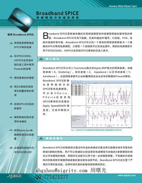
Boardband SPICE可以导入Touchstone格式或Sigrity BNP格式的网络参数,如散射参数(S,Scattering)、阻抗参数(Z, Impedance)以及导纳参数(Y,Admittance)。
这些网络参数可以由测量得到或由全波场求解器如PowerSI得到。
Boardband SPICE的输出是智能综合的SPICE等效电路模型,可以在H S p i c e 、P S p i c e 或者其他SPICE兼容的仿真器如Sigrity Speed2000中做直流、交流和瞬态分析。
使用 Broadband SPICE:将网络参数转换成SPICE等效电路在SPEED2000,HSPICE或其他时域仿真工具中使用PowerSI的结果提供紧凑的宏模型简化S参数仿真结果和测量结果的使用改善SPICE仿真的收敛性模型转换时具有宽带的准确性利用black-box电路模型增加仿真数量在频域和时域中均支持SSO的分析roadband SPICE是快速准确的实现频域模型到时域模型转换的最有效的桥B 梁。
Broadband SPICE可用于建模、仿真和描述RF器件、IC封装、PCB、电缆和接插件等对象。
Broadband SPICE可以把一个复杂的网络参数转换为一个紧凑的SPICE等效电路模型,只需要一个按钮就可以完成此操作。
得到的电路模型可用于SPEED2000,HSPICE或其他SPICE兼容的仿真工具中。
Boardband SPICE的智能综合算法和先进的曲线拟合算法使它能够完成非常复杂的频域S参数的转换。
用户可以快速的比较该等效电路模型与初始的S参数模型的响应以评估模型的精度。
局部优化功能可以用于进一步的模型调整。
子电路的内部结构和阶数是软件根据网络参数的复杂度自动调节的。
Boardband SPICE还内置了严格的无源校验功能,这样时域仿真的收敛性就能得到保证。
输入输出模型准确性Fig1. 生成的SPICE电路模型是根据初始的S参数模型拟合得来的shgzhou@ 周曙光QQ:772421277首先用PowerSI导入IC封装和PCB的设计文件,这些文件可以来自Sigrity、Cadence、Mentor Graphics、Altium和Zuken等任何一款布线产品。

Si1153 Data ShortProximity/Ambient Light Sensor IC with I 2C InterfaceThe Si1153-AA00/AA09/AA9x is an ambient light sensor, proximity, and gesture detec-tor with I 2C digital interface and programmable-event interrupt output.This touchless sensor IC includes dual 23-bit analog-to-digital converters, an integrated high-sensitivity array of visible and infrared photodiodes, a digital signal processor, and three integrated LED drivers with programmable drive levels. The Si1153 offers excel-lent performance under a wide dynamic range and a variety of light sources, including direct sunlight. The Si1153 can also work under dark glass covers. The photodiode re-sponse and associated digital conversion circuitry provide excellent immunity to artificial light flicker noise and natural light flutter noise. With two or more LEDs, the Si1153 is capable of supporting multiple-axis proximity motion detection. The Si1153 is provided in a 10-lead 2x2 mm DFN package or in a 10-lead 2.9x4.9 mm LGA module with integra-ted LED, and is capable of operation from 1.62 to 3.6 V over the –40 to +85 °C tempera-ture range.Applications:•Wearables •Handsets•Display backlighting control •Consumer electronicsLED1LED2 *LED3 **LIGHT** Pull up to VDD with 47 kOhm resistor* Pull up to VDD with 47 kOhm resistor to select primary I2C address (0x53), or down to GND for alt I2C address 0x52. Rev. 0.9Si1153 LGA Module Basic ApplicationPin Description 2.85x4.9 mm LGA ModuleSi1153 DFN Basic Application Pin Description 2x2 mm DFNTable 1.1. Recommended Operating ConditionsTable 1.2. Ordering GuideSi1153 Data Short | Smart. Connected. Energy-friendly.Rev. 0.9 | 1DisclaimerSilicon Laboratories intends to provide customers with the latest, accurate, and in-depth documentation of all peripherals and modules available for system and software implementers using or intending to use the Silicon Laboratories products. Characterization data, available modules and peripherals, memory sizes and memory addresses refer to each specific device, and "Typical" parameters provided can and do vary in different applications. Application examples described herein are for illustrative purposes only. Silicon Laboratories reserves the right to make changes without further notice and limitation to product information, specifications, and descriptions herein, and does not give warranties as to the accuracy or completeness of the included information. Silicon Laboratories shall have no liability for the consequences of use of the information supplied herein. This document does not imply or express copyright licenses granted hereunder to design or fabricate any integrated circuits. The products must not be used within any Life Support System without the specific written consent of Silicon Laboratories. A "Life Support System" is any product or system intended to support or sustain life and/or health, which, if it fails, can be reasonably expected to result in significant personal injury or death. Silicon Laboratories products are generally not intended for military applications. Silicon Laboratories products shall under no circumstances be used in weapons of mass destruction including (but not limited to) nuclear, biological or chemical weapons, or missiles capable of delivering such weapons.Trademark InformationSilicon Laboratories Inc., Silicon Laboratories, Silicon Labs, SiLabs and the Silicon Labs logo, CMEMS®, EFM, EFM32, EFR, Energy Micro, Energy Micro logo and combinations thereof, "the world’s most energy friendly microcontrollers", Ember®, EZLink®, EZMac®, EZRadio®, EZRadioPRO®, DSPLL®, ISOmodem ®, Precision32®, ProSLIC®, SiPHY®, USBXpress® and others are trademarks or registered trademarks of Silicon Laboratories Inc. ARM, CORTEX, Cortex-M3 and THUMB are trademarks or registered trademarks of ARM Holdings. Keil is a registered trademark of ARM Limited. All other products or brand names mentioned herein are trademarks of their respective holders.Silicon Laboratories Inc.400 West Cesar Chavez Austin, TX 78701USASmart.Connected.Energy-FriendlyProducts/productsQuality/qualitySupport and Community。
小信号放大电路图详解小 信号放大一直是电子设计竞赛经久不衰的题目,也是工程师们设计电路时经常遇到的问题。
作者历经小信号放大的血泪史,介绍了小信号放大中的集成芯片放大电 路、滤波器电路和分立元件放大器,有详细的电路图讲解哦!其中LC无源滤波器的软件设计、仿真以及硬件制作流程也合适很多其他电路设计。
第一部分:集成芯片放大器电路图讲解不知有多少童鞋知道TI公司的LHM6624。
这个芯片对于作者来说那是福星一枚。
其主要技术指标如下:Single/Dual Ultra Low Noise Wideband Operational Amplifier(单/双电源低噪声宽带小信号放大器);其增益带宽积在单电源供电时可达1.5GHz,双电源供电时可达1.3GHz;供电电压双电源 (± 2.5V to ± 6V)单电源(+5V to +12V);摆率(Slew rate) 350V/μs增益为10dB(AV = 10)时摆率400V/μs;输入噪声0.92nV/;输入失调电压典型值700uV 。
应用电路图如下:其中双电源供电±5V,C12,C13作用是电源滤波,即稳压;输入阻抗为50W;输出信号峰峰值可至8V(最好不要超过3V,因为大信号会出现非线性放 大)。
这是一个典型的同相放大器,放大倍数计算公式为AV=R14/R12,图中参数放大倍数20倍,即26dB。
值得注意的一点是电阻R16的作用:调 节零漂~如果对低频放大没什么特别需要的话,此处电阻R13,R16以及C11都可省略,但是如果想要放大直流信号的话,此处调节电路就十分有必要了。
模拟放大电路的电源滤波处理是十分有必要的,目的是防止高频模拟信号影响污染整个电源系统。
图中C12,C13在pcb中的位置要尽量靠近IC的电源入 口。
另外也可选择把磁珠(要求严格时可用电感,要求不高时可用100W电阻)和两个电容组成p形滤波电路, 这样可以把电源中的噪音滤得干干净净~2:滤波器滤波器分为有源滤波器和无源滤波器两种,区别在于有没有外接电源。
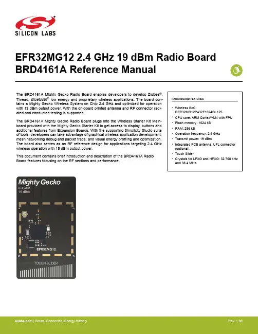
EFR32MG12 2.4 GHz 19 dBm Radio Board BRD4161A Reference ManualRADIO BOARD FEATURES•Wireless SoC:EFR32MG12P432F1024GL125•CPU core: ARM Cortex ®-M4 with FPU •Flash memory: 1024 kB •RAM: 256 kB•Operation frequency: 2.4 GHz •Transmit power: 19 dBm•Integrated PCB antenna, UFL connector (optional).•Touch Slider•Crystals for LFXO and HFXO: 32.768 kHz and 38.4 MHz.The BRD4161A Mighty Gecko Radio Board enables developers to develop Zigbee ®, Thread,Bluetooth ® low energy and proprietary wireless applications. The board con-tains a Mighty Gecko Wireless System on Chip 2.4 GHz and optimized for operation with 19 dBm output power. With the on-board printed antenna and RF connector radi-ated and conducted testing is supported.The BRD4161A Mighty Gecko Radio Board plugs into the Wireless Starter Kit Main-board provided with the Mighty Gecko Starter Kit to get access to display, buttons and additional features from Expansion Boards. With the supporting Simplicity Studio suite of tools, developers can take advantage of graphical wireless application development; mesh networking debug and packet trace; and visual energy profiling and optimization. The board also serves as an RF reference design for applications targeting 2.4 GHz wireless operation with 19 dBm output power.This document contains brief introduction and description of the BRD4161A Radio Board features focusing on the RF sections and performance.| Smart. Connected. Energy-friendly.Rev. 1.00Introduction 1. IntroductionThe EFR32 Mighty Gecko Radio Boards provide a development platform (together with the Wireless Starter Kit Mainboard) for the Silicon Labs EFR32 Mighty Gecko Wireless System on Chips and serve as reference designs for the matching network of the RF inter-face.The BRD4161A Radio Board is designed to operate in the 2400-2483.5 MHz band with the RF matching network optimized to operate with 19 dBm output power.To develop and/or evaluate the EFR32 Mighty Gecko, the BRD4161A Radio Board can be connected to the Wireless Starter Kit Main-board to get access to display, buttons and additional features from Expansion Boards and also to evaluate the performance of the RF interface.2. Radio Board Connector2.1 IntroductionThe board-to-board connector scheme allows access to all EFR32MG12 GPIO pins as well as the RESETn signal. For more informa-tion on the functions of the available pin functions, see the EFR32MG12 data sheet.2.2 Radio Board Connector Pin AssociationsThe figure below shows the pin mapping on the connector to the radio pins and their function on the Wireless Starter Kit Mainboard.GNDF9 / PA3 / VCOM_RTS 3v3VCOM_RTS / PA3 / P36P200Upper RowNC / P38NC / P40PF9 / P42PF11 / P44DEBUG.TMS_SWDIO / PF1 / F0DISP_ENABLE / PD15 / F14UIF_BUTTON0 / PF6 / F12UIF_LED1 / PF4 / F10VCOM_CTS / PA2 / F8DEBUG.RESET / RADIO_#RESET / F4DEBUG.TDO_SWO / PF2 / F2DISP_SI / PC6 / F16VCOM_TXD / PA0 / F6PTI_DATA / PB12 / F20DISP_EXTCOMIN / PD13 / F18USB_VBUS5VBoard ID SCLGNDBoard ID SDAUSB_VREG F7 / PA1 / VCOM_RXD F5 / PA5 / VCOM_ENABLE F3 / PF3 / DEBUG.TDIF1 / PF0 / DEBUG.TCK_SWCLK P45 / PF12P43 / PF10P41 / PF8P39 / NC P37/ PB10 / SENSOR_ENABLE F11 / PF5 / UIF_LED1F13 / PF7 / UIF_BUTTON1F15 / PC8 / DISP_SCLK F17 / PD14 / DISP_SCS F19 / PB13 / PTI_FRAME F21 / PB11 / PTI_CLK GND VMCU_IN PD8 / P0P201Lower RowPD9 / P2PD10 / P4PD11 / P6GNDNCP35 / PA2 / VCOM_CTS P7 / PA9P5 / PA8P3 / PA7P1 / PA6P33 / PA0 / VCOM_TXD P31 / PK2P29 / PK0P27 / PJ14P25 / PI2P23 / PI0P21 / PF14P19 / NC P17 / PC5P15 / PB9P13 / PC11P11 / PB7P9 / PB6VCOM_RXD / P34 / P34BODEN / P32PK1/ P30PJ15 / P28PI3 / P26PI1 / P24PF15 / P22PF13 / P20NC / P18PC4 / P16PB8 / P14PC10 / P12PC9 / P10PD12 / P8Figure 2.1. BRD4161A Radio Board Connector Pin MappingRadio Board Connector3. Radio Board Block Summary3.1 IntroductionThis section gives a short introduction to the blocks of the BRD4161A Radio Board.3.2 Radio Board Block DiagramThe block diagram of the EFR32MG Radio Board is shown in the figure below.Figure 3.1. BRD4161A Block Diagram3.3 Radio Board Block Description3.3.1 Wireless MCUThe BRD4161A Mighty Gecko Radio Board incorporates an EFR32MG12P432F1024GL125 Wireless System on Chip featuring 32-bit Cortex®-M4 with FPU core, 1024 kB of flash memory and 256 kB of RAM and a 2.4 GHz band transceiver with output power up to 19 dBm. For additional information on the EFR32MG12P432F1024GL125, refer to the EFR32MG12 Data Sheet.3.3.2 LF Crystal Oscillator (LFXO)The BRD4161A Radio Board has a 32.768 kHz crystal mounted.3.3.3 HF Crystal Oscillator (HFXO)The BRD4161A Radio Board has a 38.4 MHz crystal mounted.| Smart. Connected. Energy-friendly.Rev. 1.00 | 33.3.4 Matching Network for 2.4 GHzThe BRD4161A Radio Board incorporates a 2.4 GHz matching network which connects the 2.4 GHz TRX pin of the EFR32MG12 to the one on-board printed Inverted-F antenna. The component values were optimized for the 2.4 GHz band RF performace and current con-sumption with 19 dBm output power.For detailed description of the matching network, see Chapter 4.2.1 Description of the 2.4 GHz RF Matching.3.3.5 Inverted-F AntennaThe BRD4161A Radio Board includes a printed Inverted-F antenna (IFA) tuned to have close to 50 Ohm impedance at the 2.4 GHz band.For detailed description of the antenna see Chapter 4.5 Inverted-F Antenna.3.3.6 UFL ConnectorTo be able to perform conducted measurements, Silicon Labs added an UFL connector to the Radio Board. The connector allows an external 50 Ohm cable or antenna to be connected during design verification or testing.Note: By default the output of the matching network is connected to the printed Inverted-F antenna by a series component. It can be connected to the UFL connector as well through a series 0 Ohm resistor which is not mounted by default. For conducted measurements through the UFL connector the series component to the antenna should be removed and the 0 Ohm resistor should be mounted (see Chapter 4.2 Schematic of the RF Matching Network for further details).3.3.7 Radio Board ConnectorsTwo dual-row, 0.05” pitch polarized connectors make up the EFR32MG Radio Board interface to the Wireless Starter Kit Mainboard. For more information on the pin mapping between the EFR32MG12P432F1024GL125 and the Radio Board Connector, refer to Chapter 2.2 Radio Board Connector Pin Associations.3.3.8 Capacitive Touch SliderThe touch slider (T2) utilizes the capacitive touch capability of the Capacitance Sense Module of the EFR32MG12. The slider interpo-lates 4 separate pads to find the exact position of a finger.The figure below shows the pin mapping of the touch slider to the Wireless SoC.Wireless SoCFigure 3.2. Touch Slider Pin MappingRev. 1.00 | 44. RF Section4.1 IntroductionThis section gives a short introduction to the RF section of the BRD4161A.4.2 Schematic of the RF Matching NetworkThe schematic of the RF section of the BRD4161A Radio Board is shown in the following figure.2.4 GHz Matching 2.4 GHz RF OutputSelection & Inverted-F AntennaFigure 4.1. Schematic of the RF Section of the BRD4161A4.2.1 Description of the 2.4 GHz RF MatchingThe 2.4 GHz matching connects the 2G4RF_IOP pin to the on-board printed Inverted-F Antenna. The 2G4RF_ION pin is connected to ground. For higher output powers (13 dBm and above), besides the impedance matching circuitry, it is recommended to use additional harmonic filtering as well at the RF output. The targeted output power of the BRD4161A board is 19 dBm. Therefore, the RF output of the IC is connected to the antenna through a four-element impedance matching and harmonic filter circuitry.For conducted measurements the output of the matching network can also be connected to the UFL connector by removing the series R1 component between the antenna and the output of the matching and adding a 0 Ohm resistor to the R2 resistor position between the output of the matching and the UFL connector.4.3 RF Section Power SupplyOn the BRD4161A Radio Board the power supply pins of the RF section (RFVDD, PAVDD) are directly connected to the output of the on-chip DC-DC converter. This way, by default, the DC-DC converter provides 1.8 V for the entire RF section (for details, see the sche-matic of the BRD4161A).4.4 Bill of Materials for the 2.4 GHz MatchingThe Bill of Materials of the 2.4 GHz matching network of the BRD4161A Radio Board is shown in the following table.| Smart. Connected. Energy-friendly.Rev. 1.00 | 5Table 4.1. Bill of Materials for the BRD4161A 2.4GHz RF Matching Network4.5 Inverted-F AntennaThe BRD4161A Radio Board includes an on-board printed Inverted-F Antenna tuned for the 2.4 GHz band. Due to the design restric-tions of the Radio Board, the input of the antenna and the output of the matching network can't be placed directly next to each other. As a result, a 50 Ohm transmission line was necessary to connect them. With the actual line length the impedance of the antenna at the double-harmonic frequency is transformed closer to a "critical load impedance range" resulting in the radiated level of the harmonic increases.To reduce the harmonic radiation a tuning component was used between the matching network output and the antenna input. For the actual Radio Board design (with the actual transmission line length) a small value inductor was used (instead of the R1 resistor with value of 1.8 nH) to transform the impedance at the double-frequency harmonic away from the critical region while keeping the impe-dance at the funamental close to 50 Ohm. With this the suppression of the radiated double-frequency harmonic increases by approxi-mately 3-4 dB. The resulting impedance and reflection measured at the output of the matcing network are shown in the following figure. As it can be observed the impedance is close to 50 Ohm (the reflection is better than -10 dB) for the entire 2.4 GHz band.Figure 4.2. Impedance and Reflection of the Inverted-F Antenna of the BRD4161A Board Measured from the Matching Output Note: The same value and type of 1.8 nH inductor was used as the one in the matching network (L1). | Smart. Connected. Energy-friendly.Rev. 1.00 | 65. Mechanical DetailsThe BRD4161A Mighty Gecko Radio Board is illustrated in the figures below.Figure 5.1. BRD4161A Top View24 mmConnectorConnector Figure 5.2. BRD4161A Bottom ViewMechanical DetailsRev. 1.00 | 7EMC Compliance 6. EMC Compliance6.1 IntroductionCompliance of the fundamental and harmonic levels is tested against the following standards:• 2.4 GHz:•ETSI EN 300-328•FCC 15.2476.2 EMC Regulations for 2.4 GHz6.2.1 ETSI EN 300-328 Emission Limits for the 2400-2483.5 MHz BandBased on ETSI EN 300-328 the allowed maximum fundamental power for the 2400-2483.5 MHz band is 20 dBm EIRP. For the unwan-ted emissions in the 1 GHz to 12.75 GHz domain the specified limit is -30 dBm EIRP.6.2.2 FCC15.247 Emission Limits for the 2400-2483.5 MHz BandFCC 15.247 allows conducted output power up to 1 Watt (30 dBm) in the 2400-2483.5 MHz band. For spurious emmissions the limit is -20 dBc based on either conducted or radiated measurement, if the emission is not in a restricted band. The restricted bands are speci-fied in FCC 15.205. In these bands the spurious emission levels must meet the levels set out in FCC 15.209. In the range from 960 MHz to the frequency of the 5th harmonic it is defined as 0.5 mV/m at 3 m distance (equals to -41.2 dBm in EIRP).Additionally, for spurious frequencies above 1 GHz, FCC 15.35 allows duty-cycle relaxation to the regulatory limits. For the EmberZNet PRO the relaxation is 3.6 dB. Therefore, the -41.2 dBm limit can be modified to -37.6 dBm.If operating in the 2400-2483.5 MHz band the 2nd, 3rd and 5th harmonics can fall into restricted bands. As a result, for those the -37.6 dBm limit should be applied. For the 4th harmonic the -20 dBc limit should be applied.6.2.3 Applied Emission Limits for the 2.4 GHz BandThe above ETSI limits are applied both for conducted and radiated measurements.The FCC restricted band limits are radiated limits only. Besides that, Silicon Labs applies those to the conducted spectrum i.e., it is assumed that, in case of a custom board, an antenna is used which has 0 dB gain at the fundamental and the harmonic frequencies. In that theoretical case, based on the conducted measurement, the compliance with the radiated limits can be estimated.The overall applied limits are shown in the table below.Table 6.1. Applied Limits for Spurious Emissions for the 2.4 GHz Band | Smart. Connected. Energy-friendly.Rev. 1.00 | 87. RF Performance7.1 Conducted Power MeasurementsDuring measurements, the EFR32MG Radio Board was attached to a Wireless Starter Kit Mainboard which was supplied by USB. The voltage supply for the Radio Board was 3.3 V.7.1.1 Conducted Measurements in the 2.4 GHz bandThe BRD4161A board was connected directly to a Spectrum Analyzer through its UFL connector (the R1 component was removed and a 0 Ohm resistor was soldered to the R2 resistor position). During measurements, the voltage supply for the board was 3.3 V provided by the mainboard. The supply for the radio (RFVDD) was 1.8 V provided by the on-chip DC-DC converter, the supply for the power amplifier (PAVDD) was 3.3 V (for details, see the schematic of the BRD4161A). The transceiver was operated in continuous carrier transmission mode. The output power of the radio was set to 19 dBm.The typical output spectrum is shown in the following figure.Figure 7.1. Typical Output Spectrum of the BRD4161AAs it can be observed, the fundamental is slightly lower than 19 dBm limit and the strongest unwanted emission is the double-frequency harmonic and it is under the -37.6 dBm applied limit.Note: The conducted measurement is performed by connecting the on-board UFL connector to a Spectrum Analyzer through an SMA Conversion Adapter (P/N: HRMJ-U.FLP(40)). This connection itself introduces approximately 0.3 dB insertion loss.RF PerformanceRev. 1.00 | 97.2 Radiated Power MeasurementsDuring measurements, the EFR32MG Radio Board was attached to a Wireless Starter Kit Mainboard which was supplied by USB. The voltage supply for the Radio Board was 3.3 V. The radiated power was measured in an antenna chamber by rotating the DUT 360degrees with horizontal and vertical reference antenna polarizations in the XY , XZ and YZ cuts. The measurement axes are shown inthe figure below.Figure 7.2. DUT: Radio Board with the Wireless Starter Kit Mainboard (Illustration)Note: The radiated measurement results presented in this document were recorded in an unlicensed antenna chamber. Also the radi-ated power levels may change depending on the actual application (PCB size, used antenna, and so on). Therefore, the absolute levels and margins of the final application are recommended to be verified in a licensed EMC testhouse.7.2.1 Radiated Measurements in the 2.4 GHz bandFor the transmitter antenna the on-board printed Inverted-F antenna of the BRD4161A board was used (the R1 component was moun-ted). During measurements, the board was attached to a Wireless Starter Kit Mainboard (BRD4001 (Rev. A02) ) which was supplied through USB. During the measurements the voltage supply for the board was 3.3 V provided by the mainboard. The supply for the radio (RFVDD) was 1.8 V provided by the on-chip DC-DC converter, the supply for the power amplifier (PAVDD) was 3.3 V (for details, see the schematic of the BRD4161A). The transceiver was operated in continuous carrier transmission mode. The output power of the radio was set to 19 dBm based on the conducted measurement.The results are shown in the table below.Table 7.1. Maximums of the measured radiated powers in EIRP [dBm]As it can be observed, thanks to the high gain of the Inverted-F antenna, the level of the fundamental is higher than 19 dBm. The stron-gest harmonic is the double-frequency one and thanks to the additional suppression provided by the instead of the R1 resistor its level is under -50 dBm.RF PerformanceEMC Compliance Recommendations 8. EMC Compliance Recommendations8.1 Recommendations for 2.4 GHz ETSI EN 300-328 complianceAs it was shown in the previous chapter, the radiated power of the fundamental of the BRD4161A Mighty Gecko Radio Board complies with the 20 dBm limit of the ETSI EN 300-328 in case of the conducted measurement but due to the high antenna gain the radiated power is higher than the limit by 2 dB. In order to comply, the output power should be reduced (with different antennas, depending on the gain of the used antenna, the necessary reduction can be different). The harmonic emissions are under the -30 dBm limit. Although the BRD4161A Radio Board has an option for mounting a shielding can, that is not required for the compliance.8.2 Recommendations for 2.4 GHz FCC 15.247 complianceAs it was shown in the previous chapter, the radiated power of the fundamental of the BRD4161A Mighty Gecko Radio Board complies with the 30 dBm limit of the FCC 15.247. The harmonic emissions are under the -37.6 dBm applied limit both in case of the conducted and the radiated measurements. Although the BRD4161A Radio Board has an option for mounting a shielding can, that is not required for the compliance.Document Revision History 9. Document Revision HistoryTable 9.1. Document Revision HistoryBoard Revision History 10. Board Revision HistoryTable 10.1. BRD4161A Radio Board RevisionsErrata 11. ErrataThere are no known errata at present.Table of Contents1. Introduction (1)2. Radio Board Connector (2)2.1 Introduction (2)2.2 Radio Board Connector Pin Associations (2)3. Radio Board Block Summary (3)3.1 Introduction (3)3.2 Radio Board Block Diagram (3)3.3 Radio Board Block Description (3)3.3.1 Wireless MCU (3)3.3.2 LF Crystal Oscillator (LFXO) (3)3.3.3 HF Crystal Oscillator (HFXO) (3)3.3.4 Matching Network for 2.4 GHz (4)3.3.5 Inverted-F Antenna (4)3.3.6 UFL Connector (4)3.3.7 Radio Board Connectors (4)3.3.8 Capacitive Touch Slider (4)4. RF Section (5)4.1 Introduction (5)4.2 Schematic of the RF Matching Network (5)4.2.1 Description of the 2.4 GHz RF Matching (5)4.3 RF Section Power Supply (5)4.4 Bill of Materials for the 2.4 GHz Matching (5)4.5 Inverted-F Antenna (6)5. Mechanical Details (7)6. EMC Compliance (8)6.1 Introduction (8)6.2 EMC Regulations for 2.4 GHz (8)6.2.1 ETSI EN 300-328 Emission Limits for the 2400-2483.5 MHz Band (8)6.2.2 FCC15.247 Emission Limits for the 2400-2483.5 MHz Band (8)6.2.3 Applied Emission Limits for the 2.4 GHz Band (8)7. RF Performance (9)7.1 Conducted Power Measurements (9)7.1.1 Conducted Measurements in the 2.4 GHz band (9)7.2 Radiated Power Measurements (10)7.2.1 Radiated Measurements in the 2.4 GHz band (10)8. EMC Compliance Recommendations (11)8.1 Recommendations for 2.4 GHz ETSI EN 300-328 compliance (11)8.2 Recommendations for 2.4 GHz FCC 15.247 compliance (11)9. Document Revision History (12)10. Board Revision History (13)11. Errata (14)Table of Contents (15)Silicon Laboratories Inc.400 West Cesar Chavez Austin, TX 78701USASimplicity StudioOne-click access to MCU and wireless tools, documentation, software, source code libraries & more. Available for Windows, Mac and Linux!IoT Portfolio /IoTSW/HW/simplicityQuality/qualitySupport and CommunityDisclaimerSilicon Labs intends to provide customers with the latest, accurate, and in-depth documentation of all peripherals and modules available for system and software implementers using or intending to use the Silicon Labs products. Characterization data, available modules and peripherals, memory sizes and memory addresses refer to each specific device, and "Typical" parameters provided can and do vary in different applications. Application examples described herein are for illustrative purposes only. Silicon Labs reserves the right to make changes without further notice and limitation to product information, specifications, and descriptions herein, and does not give warranties as to the accuracy or completeness of the included information. Silicon Labs shall have no liability for the consequences of use of the information supplied herein. This document does not imply or express copyright licenses granted hereunder to design or fabricate any integrated circuits. The products are not designed or authorized to be used within any Life Support System without the specific written consent of Silicon Labs. A "Life Support System" is any product or system intended to support or sustain life and/or health, which, if it fails, can be reasonably expected to result in significant personal injury or death. Silicon Labs products are not designed or authorized for military applications. Silicon Labs products shall under no circumstances be used in weapons of mass destruction including (but not limited to) nuclear, biological or chemical weapons, or missiles capable of delivering such weapons.Trademark InformationSilicon Laboratories Inc.® , Silicon Laboratories®, Silicon Labs®, SiLabs® and the Silicon Labs logo®, Bluegiga®, Bluegiga Logo®, Clockbuilder®, CMEMS®, DSPLL®, EFM®, EFM32®, EFR, Ember®, Energy Micro, Energy Micro logo and combinations thereof, "the world’s most energy friendly microcontrollers", Ember®, EZLink®, EZRadio®, EZRadioPRO®, Gecko®, ISOmodem®, Precision32®, ProSLIC®, Simplicity Studio®, SiPHY®, Telegesis, the Telegesis Logo®, USBXpress® and others are trademarks or registered trademarks of Silicon Labs. ARM, CORTEX, Cortex-M3 and THUMB are trademarks or registered trademarks of ARM Holdings. Keil is a registered trademark of ARM Limited. All other products or brand names mentioned herein are trademarks of their respective holders.。

Canddence Sigrity中用Power SI进行走线阻抗与耦合检查分析(组件ERC->Trace Imp/cpl/ref check)基于信号完整性考虑,检查PCB阻抗和其耦合串扰是否满足要求,是硬件工程师的必要工作。
对于有较多高速或信号线的PCB来说,手动检查费时费力效果也不好,非常容易漏掉一些关键点,有必要寻找一种自动检查的方法。
如下介绍基于仿真软件Sigrity的自动检查,其快速、准确,不仅降低了工程师的工作量,且改善了检查的结果,有利于PCB的优化。
Sigrity软件Power SI进行走线阻抗与耦合检查分析有两点需要注意:第一个是这个功能计算出来的阻抗和SI9000会有一点偏差。
第二个是其耦合度检查只能检查同层之间的耦合,对于不同层之间的耦合还无法进行检查。
不过在绝大多数的设计中,现有的这个功能已经够用了,通过这个方式可以非常快速的对整版或是重点关注的信号进行阻抗及耦合的检查,找到设计的薄弱环节进行整改。
3.2.1 阻抗和耦合阻抗:在具有电阻、电感和电容的电路里,对交流电所起的阻碍作用叫做阻抗。
阻抗常用Z 表示;的复杂性、调用模块的方式以及通过界面传送数据的多少?2片32位DDR3阻抗和耦合分析为例3.3 以仿XC7Z010CLG400与修改成实际的板厚、基材等信息。
要根据厂家的信息来填写。
材料参数:可以通过view Material按钮查看。
焊盘的设置:环氧树脂是BT;Er为材料的介电常数;Loss tangent损耗因数;Detect and model the coplanar traces共面轨迹的检测与建模>Setup 选取器件:器件选择把要仿真的网络对应的器件(这里面我们选端要赋予正极的标注。
选择发送端芯片或内存控制器或者直接找,输入U1;网络我们之前已经选择过,该步骤直接跳过,点击下一步。
串阻之间的value值需要补上,根据实际情况,比如22欧姆或33欧姆。
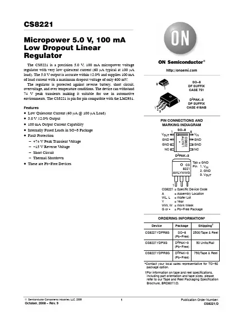
CS8221Micropower 5.0 V, 100 mA Low Dropout Linear RegulatorThe CS8221 is a precision 5.0 V, 100 mA micropower voltage regulator with very low quiescent current (60 m A typical at 100 m A load). The 5.0 V output is accurate within ±2.0% and supplies 100 mA of load current with a maximum dropout voltage of only 600 mV. The regulator is protected against reverse battery, short circuit, overvoltage, and over temperature conditions. The device can withstand 74 V peak transients making it suitable for use in automotive environments. The CS8221 is pin for pin compatible with the LM2931. Features•Low Quiescent Current (60 m A @ 100 m A Load)•5.0 V ±2.0% Output•100 mA Output Current Capability •Internally Fused Leads in SO−8 Package •Fault Protection−+74 V Peak Transient V oltage−−15 V Reverse V oltage−Short Circuit−Thermal Shutdown•These are Pb−Free DevicesPIN CONNECTIONS ANDMARKING INDIAGRAMDevice Package Shipping†ORDERING INFORMATION*D2PAK−3(Pb−Free)CS8221YDP3G50 Units/RailCS8221= Specific Device CodeA= Assembly LocationWL, L= Wafer LotY= YearWW, W= Work WeekG or G= Pb−Free PackageSO−8DF SUFFIXCASE 751INVCS8221AWLYWWG1Tab = GNDPin 1. V IN2. GND3. V OUTD2PAK−3CS8221YDPR3G D2PAK−3(Pb−Free)750/T ape & Reel*Contact your local sales representative for TO−92 package option.†For information on tape and reel specifications, including part orientation and tape sizes, please refer to our Tape and Reel Packaging Specification Brochure, BRD8011/D.D2PAK−3DP SUFFIXCASE 418ABCS8221YDFR8G2500/T ape & ReelSO−8(Pb−Free)Figure 1. Block DiagramGNDV OUTV INABSOLUTE MAXIMUM RATINGS*RatingValue Unit Junction Temperature Range, T J−40 to +150°C Storage Temperature Range, T STORAGE −55 to +150°C Power DissipationInternally Limited−Peak Transient Voltage (60 V Load Dump @ V IN = 14 V)−15, 74V Input Operating Range −0.5 to 26V Output CurrentInternally Limited−Electrostatic Discharge (Human Body Model) 2.0kV Lead Temperature Soldering:Reflow (Note 1)230 peak°CStresses exceeding Maximum Ratings may damage the device. Maximum Ratings are stress ratings only. Functional operation above the Recommended Operating Conditions is not implied. Extended exposure to stresses above the Recommended Operating Conditions may affect device reliability.1.60 seconds maximum above 183°.*The maximum package power dissipation must be observed.ELECTRICAL CHARACTERISTICS (6.0 ≤ V IN ≤26 V , I OUT = 1.0 mA, −40°C ≤ T J ≤125°C unless otherwise noted.)CharacteristicTest ConditionsMinTypMaxUnitOutput Stage Output Voltage, V OUT9.0 V < V IN < 26 V, 100 m A ≤I OUT ≤ 100 mA 6.0 V ≤ V IN ≤ 26 V, 100 m A ≤I OUT ≤ 100 mA 4.94.85 5.05.0 5.15.15V V Dropout Voltage (V IN − V OUT )I OUT = 100 mA I OUT = 100 m A−−400100600150mV mV Load Regulation V IN = 14 V , 100 m A ≤I OUT ≤100 mA,− 5.050mV Line Regulation 6.0 V < V < 26 V, I OUT = 1.0 mA − 5.050mV Quiescent Current, (I Q )I OUT = 100 m A, V IN = 6.0 V I OUT = 50 mA I OUT = 100 mA−−−604.0121206.020m A mA mA Ripple Rejection 7.0 ≤ V IN ≤ 17 V , I OUT = 100 mA, f = 120 Hz6075−dB Current Limit−125200−mAShort Circuit Output Current V OUT = 0 V40125−m A Thermal Shutdown (Note 2)−150180−°C Overvoltage ShutdownV OUT ≤ 1.0 V303438V2.This parameter is guaranteed by design, but not parametrically tested in production.PACKAGE LEAD DESCRIPTIONPACKAGE LEAD #LEAD SYMBOLFUNCTIONSO −8D 2PAK −313V OUT 5.0 V, ±2.0%, 100 mA Output.2, 3, 6, 72GND Ground.4−NC No Connection.5−NC No Connection.81V INInput Voltage.TYPICAL PERFORMANCE CHARACTERISTICSFigure 2. CS8221 Output StabilityE S R (W )I OUT OUTPUT CURRENTCIRCUIT DESCRIPTIONVOLTAGE REFERENCE AND OUTPUT CIRCUITRY Output Stage ProtectionThe output stage is protected against overvoltage, short circuit and thermal runaway conditions (Figure 3).Figure 3. Typical Circuit Waveforms for OutputStage ProtectionILoad DumpV VThermal ShutdownShort CircuitIf the input voltage rises above 30 V , the output shuts down. This response protects the internal circuitry and enables the IC to survive unexpected voltage transients.Should the junction temperature of the power device exceed 180°C (typ) the power transistor is turned off.Thermal shutdown is an effective means to prevent die overheating since the power transistor is the principle heat source in the IC.Figure 4. Application and Test Diagram*C 1 is required if regulator is far from the power source filter .**C 2 is required for stability.APPLICATION NOTESSTABILITY CONSIDERATIONSThe output or compensation capacitor helps determine three main characteristics of a linear regulator: start −up delay, load transient response and loop stability.The capacitor value and type should be based on cost,availability, size and temperature constraints. A tantalum or aluminum electrolytic capacitor is best, since a film or ceramic capacitor with almost zero ESR can cause instability. The aluminum electrolytic capacitor is the least expensive solution, but, if the circuit operates at low temperatures (−25°C to −40°C), both the value and ESR of the capacitor will vary considerably. The capacitor manufacturers data sheet usually provides this information.The value for the output capacitor C OUT shown in Figure 4 should work for most applications, however it is not necessarily the optimized solution.To determine an acceptable value for C OUT for a particular application, start with a tantalum capacitor of the recommended value and work towards a less expensive alternative part.Step 1: Place the completed circuit with a tantalum capacitor of the recommended value in an environmental chamber at the lowest specified operating temperature and monitor the outputs with an oscilloscope. A decade box connected in series with the capacitor will simulate the higher ESR of an aluminum capacitor. Leave the decade box outside the chamber, the small resistance added by the longer leads is negligible.Step 2: With the input voltage at its maximum value,increase the load current slowly from zero to full load while observing the output for any oscillations. If no oscillations are observed, the capacitor is large enough to ensure a stable design under steady state conditions.Step 3: Increase the ESR of the capacitor from zero using the decade box and vary the load current until oscillations appear. Record the values of load current and ESR that cause the greatest oscillation. This represents the worst case load conditions for the regulator at low temperature.Step 4: Maintain the worst case load conditions set in step 3 and vary the input voltage until the oscillations increase. This point represents the worst case input voltage conditions.Step 5: If the capacitor is adequate, repeat steps 3 and 4with the next smaller valued capacitor. A smaller capacitor will usually cost less and occupy less board space. If the output oscillates within the range of expected operating conditions, repeat steps 3 and 4 with the next larger standard capacitor value.Step 6: Test the load transient response by switching in various loads at several frequencies to simulate its real working environment. Vary the ESR to reduce ringing.Step 7: Increase the temperature to your highest operating temperature. V ary the load current as instructed in step 5 to test for any oscillations.Once the minimum capacitor value with the maximum ESR is found, a safety factor should be added to allow for the tolerance of the capacitor and any variations in regulator performance. Most good quality aluminum electrolytic capacitors have a tolerance of ± 20% so the minimum value found should be increased by at least 50% to allow for this tolerance plus the variation which will occur at low temperatures. The ESR of the capacitor should be less than 50% of the maximum allowable ESR found in step 3 above.CALCULATING POWER DISSIPATION IN A SINGLEOUTPUT LINEAR REGULATORThe maximum power dissipation for a single output regulator (Figure 5) is:P D(max)+NJV IN(max)*V OUT(min)NjI OUT(max))V IN(max)I Q(1)where:V IN(max) is the maximum input voltage,V OUT(min) is the minimum output voltage,I OUT(max) is the maximum output current for the application, andI Q is the quiescent current the regulator consumes at I OUT(max).Once the value of P D(max) is known, the maximum permissible value of R ΘJA can be calculated:R Q JA +(2)The value of R ΘJA can then be compared with those in the package section of the data sheet. Those packages with R ΘJA ’s less than the calculated value in equation 2 will keep the die temperature below 150°C.In some cases, none of the packages will be sufficient to dissipate the heat generated by the IC, and an external heatsink will be required.Figure 5. Single Output Regulator With KeyPerformance Parameters LabeledV INV OUTHEAT SINKSA heat sink effectively increases the surface area of the package to improve the flow of heat away from the IC and into the surrounding air.Each material in the heat flow path between the IC and the outside environment will have a thermal resistance. Like series electrical resistances, these resistances are summed to determine the value of R ΘJA .R Q JA +R Q JC )R Q CS )R Q SA(3)where:R ΘJC = the junction −to −case thermal resistance,R ΘCS = the case −to −heatsink thermal resistance, and R ΘSA = the heatsink −to −ambient thermal resistance.R ΘJC appears in the package section of the data sheet. Like R ΘJA , it too is a function of package type. R ΘCS and R ΘSA are functions of the package type, heatsink and the interface between them. These values appear in heat sink data sheets of heat sink manufacturers.SMART REGULATOR is a registered trademark of Semiconductor Components Industries, LLC (SCILLC).MECHANICAL CASE OUTLINE PACKAGE DIMENSIONSON Semiconductor and are registered trademarks of Semiconductor Components Industries, LLC (SCILLC). SCILLC reserves the right to make changes without further notice to any products herein. SCILLC makes no warranty, representation or guarantee regarding the suitability of its products for any particular purpose, nor does SCILLC assume any liability arising out of the application or use of any product or circuit, and specifically disclaims any and all liability, including without limitation special, consequential or incidental damages.“Typical” parameters which may be provided in SCILLC data sheets and/or specifications can and do vary in different applications and actual performance may vary over time. All operating parameters, including “Typicals” must be validated for each customer application by customer’s technical experts. SCILLC does not convey any license under its patent rights nor the rights of others. SCILLC products are not designed, intended, or authorized for use as components in systems intended for surgical implant into the body, or other applications intended to support or sustain life, or for any other application in which the failure of the SCILLC product could create a situation where personal injury or death may occur. Should Buyer purchase or use SCILLC products for any such unintended or unauthorized application, Buyer shall indemnify and hold SCILLC and its officers, employees, subsidiaries, affiliates,and distributors harmless against all claims, costs, damages, and expenses, and reasonable attorney fees arising out of, directly or indirectly, any claim of personal injury or deathSOIC −8 NB CASE 751−07ISSUE AKDATE 16 FEB 2011NOTES:1.DIMENSIONING AND TOLERANCING PER ANSI Y14.5M, 1982.2.CONTROLLING DIMENSION: MILLIMETER.3.DIMENSION A AND B DO NOT INCLUDE MOLD PROTRUSION.4.MAXIMUM MOLD PROTRUSION 0.15 (0.006)PER SIDE.5.DIMENSION D DOES NOT INCLUDE DAMBAR PROTRUSION. ALLOWABLE DAMBARPROTRUSION SHALL BE 0.127 (0.005) TOTAL IN EXCESS OF THE D DIMENSION AT MAXIMUM MATERIAL CONDITION.6.751−01 THRU 751−06 ARE OBSOLETE. NEW STANDARD IS 751−07.SCALE 1:1STYLES ON PAGE 2DIM A MIN MAX MIN MAX INCHES4.805.000.1890.197MILLIMETERSB 3.80 4.000.1500.157C 1.35 1.750.0530.069D 0.330.510.0130.020G 1.27 BSC 0.050 BSC H 0.100.250.0040.010J 0.190.250.0070.010K 0.40 1.270.0160.050M 0 8 0 8 N 0.250.500.0100.020S5.806.200.2280.244MYM0.25 (0.010)YM0.25 (0.010)Z SXS____XXXXX = Specific Device Code A = Assembly Location L = Wafer Lot Y = YearW = Work WeekG = Pb −Free PackageGENERICMARKING DIAGRAM*8ICDiscrete 0.60.024ǒmm inchesǓSCALE 6:1*For additional information on our Pb −Free strategy and soldering details, please download the ON Semiconductor Soldering and Mounting Techniques Reference Manual, SOLDERRM/D.SOLDERING FOOTPRINT*Discrete(Pb −Free)IC (Pb −Free)XXXXXX = Specific Device Code A = Assembly Location Y = Year WW = Work Week G = Pb −Free Package*This information is generic. Please refer todevice data sheet for actual part marking.Pb −Free indicator, “G” or microdot “G ”, may or may not be present. Some products may not follow the Generic Marking.MECHANICAL CASE OUTLINEPACKAGE DIMENSIONSSOIC −8 NB CASE 751−07ISSUE AKDATE 16 FEB 2011STYLE 4:PIN 1.ANODE2.ANODE3.ANODE4.ANODE5.ANODE6.ANODE7.ANODEMON CATHODE STYLE 1:PIN 1.EMITTER2.COLLECTOR3.COLLECTOR4.EMITTER5.EMITTER6.BASE7.BASE8.EMITTER STYLE 2:PIN 1.COLLECTOR, DIE, #12.COLLECTOR, #13.COLLECTOR, #24.COLLECTOR, #25.BASE, #26.EMITTER, #27.BASE, #18.EMITTER, #1STYLE 3:PIN 1.DRAIN, DIE #12.DRAIN, #13.DRAIN, #24.DRAIN, #25.GATE, #26.SOURCE, #27.GATE, #18.SOURCE, #1STYLE 6:PIN 1.SOURCE2.DRAIN3.DRAIN4.SOURCE5.SOURCE6.GATE7.GATE8.SOURCE STYLE 5:PIN 1.DRAIN2.DRAIN3.DRAIN4.DRAIN5.GATE6.GATE7.SOURCE8.SOURCESTYLE 7:PIN 1.INPUT2.EXTERNAL BYPASS3.THIRD STAGE SOURCE4.GROUND5.DRAIN6.GATE 37.SECOND STAGE Vd 8.FIRST STAGE Vd STYLE 8:PIN 1.COLLECTOR, DIE #12.BASE, #13.BASE, #24.COLLECTOR, #25.COLLECTOR, #26.EMITTER, #27.EMITTER, #18.COLLECTOR, #1STYLE 9:PIN 1.EMITTER, COMMON2.COLLECTOR, DIE #13.COLLECTOR, DIE #24.EMITTER, COMMON5.EMITTER, COMMON6.BASE, DIE #27.BASE, DIE #18.EMITTER, COMMON STYLE 10:PIN 1.GROUND2.BIAS 13.OUTPUT4.GROUND5.GROUND6.BIAS 27.INPUT8.GROUND STYLE 11:PIN 1.SOURCE 12.GATE 13.SOURCE 24.GATE 25.DRAIN 26.DRAIN 27.DRAIN 18.DRAIN 1STYLE 12:PIN 1.SOURCE2.SOURCE3.SOURCE4.GATE5.DRAIN6.DRAIN7.DRAIN8.DRAINSTYLE 14:PIN 1.N −SOURCE2.N −GATE3.P −SOURCE4.P −GATE5.P −DRAIN6.P −DRAIN7.N −DRAIN8.N −DRAIN STYLE 13:PIN 1.N.C.2.SOURCE3.SOURCE4.GATE5.DRAIN6.DRAIN7.DRAIN8.DRAIN STYLE 15:PIN 1.ANODE 12.ANODE 13.ANODE 14.ANODE 15.CATHODE, COMMON6.CATHODE, COMMON7.CATHODE, COMMON8.CATHODE, COMMON STYLE 16:PIN 1.EMITTER, DIE #12.BASE, DIE #13.EMITTER, DIE #24.BASE, DIE #25.COLLECTOR, DIE #26.COLLECTOR, DIE #27.COLLECTOR, DIE #18.COLLECTOR, DIE #1STYLE 17:PIN 1.VCC2.V2OUT3.V1OUT4.TXE5.RXE6.VEE7.GND8.ACCSTYLE 18:PIN 1.ANODE2.ANODE3.SOURCE4.GATE5.DRAIN6.DRAIN7.CATHODE8.CATHODESTYLE 19:PIN 1.SOURCE 12.GATE 13.SOURCE 24.GATE 25.DRAIN 26.MIRROR 27.DRAIN 18.MIRROR 1STYLE 20:PIN 1.SOURCE (N)2.GATE (N)3.SOURCE (P)4.GATE (P)5.DRAIN6.DRAIN7.DRAIN8.DRAIN STYLE 21:PIN 1.CATHODE 12.CATHODE 23.CATHODE 34.CATHODE 45.CATHODE 5MON ANODEMON ANODE8.CATHODE 6STYLE 22:PIN 1.I/O LINE 1MON CATHODE/VCCMON CATHODE/VCC4.I/O LINE 3MON ANODE/GND6.I/O LINE 47.I/O LINE 5MON ANODE/GND STYLE 23:PIN 1.LINE 1 INMON ANODE/GNDMON ANODE/GND4.LINE 2 IN5.LINE 2 OUTMON ANODE/GNDMON ANODE/GND8.LINE 1 OUT STYLE 24:PIN 1.BASE2.EMITTER3.COLLECTOR/ANODE4.COLLECTOR/ANODE5.CATHODE6.CATHODE7.COLLECTOR/ANODE 8.COLLECTOR/ANODE STYLE 25:PIN 1.VIN2.N/C3.REXT4.GND5.IOUT6.IOUT7.IOUT8.IOUTSTYLE 26:PIN 1.GND2.dv/dt3.ENABLE4.ILIMIT5.SOURCE6.SOURCE7.SOURCE8.VCCSTYLE 27:PIN 1.ILIMIT2.OVLO3.UVLO4.INPUT+5.SOURCE6.SOURCE7.SOURCE8.DRAINSTYLE 28:PIN 1.SW_TO_GND2.DASIC_OFF3.DASIC_SW_DET4.GND5.V_MON6.VBULK7.VBULK8.VINSTYLE 29:PIN 1.BASE, DIE #12.EMITTER, #13.BASE, #24.EMITTER, #25.COLLECTOR, #26.COLLECTOR, #27.COLLECTOR, #18.COLLECTOR, #1STYLE 30:PIN 1.DRAIN 12.DRAIN 13.GATE 24.SOURCE 25.SOURCE 1/DRAIN 26.SOURCE 1/DRAIN 27.SOURCE 1/DRAIN 28.GATE 1PUBLICATION ORDERING INFORMATIONTECHNICAL SUPPORTLITERATURE FULFILLMENT:。
PowerSI高效的电磁场分析技术为IC封装和PCB设计提供了全波分析的精度。
其优秀的效率和精度是因为PowerSI采用了Sigrity公司独特的专利分析技术,在对平面的分割、开槽,多层电源地平面的叠层,大量的过孔和走线等复杂结构进行精确模型时使用了自适应的数值网格剖分技术。
PowerSI还提供了智能的多CPU仿真技术,可以把一个大型的复杂任务分配给多个CPU同步完成,从而大大提高了仿真效率。
使用PowerSI:提取PCB和IC封装的散射S参数和阻抗Z参数分析电源&信号网络的谐振特性,提出改进的方案评估去耦电容的不同放置方案对PI的影响分析不同电路结构(平面、走线、过孔)间的电磁耦合分析信号回流路径的不连续性分析PDS随频域变化的空间噪声分布和谐振点分布分析近场和远场的EMI& EMC辐射与Broadband SPICE配合,生成宽带的SPICE电路模型owerSI可以为IC封装和PCB设计提供快速准确的全波电磁场分析,从而P 解决高速电路设计中日益突出的各种PI和SI问题:如同步切换噪声(SSN)问题,信号耦合问题,去耦电容放置不当问题以及电压超标问题等。
PowerSI可以在布局布线前用于创建PI和SI的布线规范,也可以在布局布线后用于发现或改善潜在的设计风险。
与传统的SI分析工具不同的是:PowerSI不是将电源地平面当作理想平面来处理,而是充分考虑了电源地平面上实际物理结构的影响。
同时PowerSI可以直接做整板仿真,而无需像一些传统的纯3D仿真工具那样,仿真前把板子切成很多小块分别做模型提取,这样既提高了仿真精度也减少了模型操作的时间。
快速准确特色优势先进的分析技术Fig1. 系统级电源网络的参数提取shgzhou@ 周曙光 QQ:772421277当前设计人员常常要求以尽可能低的成本设计出合格的产品,而PowerSI可以帮助他们尽早的发现设计风险并找到解决方案。
及时的解决EMI问题对改善PI和SI的性能是至关重要的,PowerSI的近场和远场分析功能除了精度上经过充分的验证之外,其直观的3D结果显示还直接与PCB的结构相对应。

D a t a S h e e t -2020.03SHS800 Series Handheld Digital OscilloscopeWWW.SIGLENT .COMApplication Domain• Outdoor measure • Circuit measure• Wind power, PV power and other new energy equipment test• Automotive electron, electric automobile test • Electric power system,strong electricity test• Industry scenes electric debug testing and measuring • Education and science research • Quality controlFeatures & BenefitsDual-input,combine oscilloscope, Multimeter and recorder (including TrendPlot and waveform Recorder) in one unitInput voltage: input voltage through BNC is up to CAT Ⅱ 300V and CAT Ⅲ 150VStandard probe: 10X CATII 300V and 1X CATII 150V Optional probe: 10X CAT Ⅱ 1000V and 10X CAT Ⅲ 600V Oscilloscope and multimeter safety grade is up to CAT Ⅱ 600V and CAT Ⅲ 300V 5.7 inch TFT color LCD displayMax. 200MHz Bandwidth, 1GSa/s real-time sampling rate single channel, up to 50GSa/s equivalent sampling rate With 6000 dots display resolution Multimeter and provides measurements of DCV , ACV , DCI, ACI, Resistance, Diode, Capacitance and ContinuitySupport Scope TrendPlot, Meter TrendPlot and Scope RecorderTrigger modes :Automatic , Normal and SingleTrigger types: Edge, Pulse, Video,Slope and Alternative 32 automatic measurements,3 cursor measure modes 4 digital filter mode: Low pass,High pass, Band pass, Band limitMath functions: +, - , ×, ÷, FFT operations Multiple Language User InterfaceStandard configuration interface: USB Device,USB Host Support USB storage and updateRechargeable Li battery pack,compact,portable,fit for outdoor operationWWW.SIGLENT .COMSHS800 Series Handheld Digital Oscilloscope• Scope TrendPlot records scope measurement data, 800K points capacity, more than 18 hours recording time • Meter TrendPlot records multimeter measurement data, 1.2M points recording length, recording time as long as 6000 hours at 0.05Sa/s• Real-time saving measuring data,which can be outputted to U memery,used for second research and analying • Two display modes, ‘ALL’ and ‘NORMAL’; support zoom and cursor • Support recording real time• Recording scope waveform continually in scan mode • Support recording, replay and zoom function • 7M points memory depth,18 hours recording time• Maximum 4GB in USB storage mode, 3000hours recording time• 6000 counts high percison Multimeter• Providing measurements of DCV , ACV , DCI, ACI, Resistance, Diode, Capacitance, ContinuityTrendPlotScope RecorderMultimeterScope TrendPlot DCV measurement Meter TrendPlotACI measurementSHS800 Series Handheld Digital OscilloscopeWWW.SIGLENT .COMSHS800 Series Handheld Digital OscilloscopeTechnical SpecificationsNote: [1], [2] For rank A range, the measurement time should be less than 10s, the interval time should be more than 15 minutes.• OscilloscopeSHS800 Series Handheld Digital OscilloscopeWWW.SIGLENT.COMSHS800 Series Handheld Digital Oscilloscope• Multimeter• RecorderSHS800 Series Handheld Digital OscilloscopeWWW.SIGLENT.COMGeneric SpecificationWWW.SIGLENT .COMSHS800 Series Handheld Digital OscilloscopeOrdering InformationFacebook: SiglentTech。
Rev. 1.2 12/15Copyright © 2015 by Silicon LaboratoriesSi4356RXModule-UGU SERS ’ G UIDE1. OverviewThis document describes the basic use of the 4356-RX-434 small standalone receiver module. The schematic of the module is shown in Figure 1.Figure 1.4356-RX-434 Standalone Receiver Module SchematicThe module contains the Si4356 Standalone Sub-GHz Receiver RF IC, a Zener diode or LDO, a low-cost SMD crystal, and the 4-element discrete matching balun transformer. Because the Si4356 RF IC is pin configurable, the module can operate in RX mode with different configurations. Different carrier frequencies, data rates, modulation types, frequency deviations, and receiver bandwidths can be set by the configuration selector pins (SEL0–SEL3).These pins are connected to GND, VDD_RF, OUT0 (pin 12), or OUT1 (pin 14). The Si4356 provides the received RAW data on pin 14.The receiver performance can be significantly improved by adding a low-pass filter to the RX data output. These optional RC components are represented by R3 and C5 in Figure 1. Component values have to be calculated based on the expected data rate, where DR=1/(2*pi*R*C). For 2.4kbps, a good combination could be 1k with 47nF. For 1kbps, use 100nF.The element values of the 4-element discrete matching balun transformer depend on the operating frequency. TheN o r t Re co m m e nd edf or Ne w De si g n sSi4356RXModule-UGelement values can be found in the Si4356 data sheet and are detailed in “AN643: Si446x/Si4362 RX LNA Matching”.The module is +5V compatible; therefore, supply voltages up to +5V can be connected to the VDD. Meanwhile,the Si4356 RF IC does not tolerate voltages above +3.6V (VDD_RF). This voltage conversion between the VDD and VDD_RF (see Figure 1) is ensured by a Zener diode or an LDO; one of them should be mounted simultaneously. Do not directly connect +5V to the pins of the Si4356 RF IC! The default and typical supply voltage for the VDD is +5V while using an LDO to drive 3.3V for the Si4356 RF IC (VDD_RF). If using a Zener diode, the R1 resistor value must be determined according to the Zener diode and the supply voltages.The RST pin of the Si4356 RF IC on the small RX module is directly connected to the GND, which means that it is not possible to reset the radio chip externally. For this reason, it is strongly recommended to ensure the exact VDD requirements for the radio chip for a proper power-on-reset (POR), as documented in the Si4356 data sheet.If the documented radio VDD requirements are not carefully followed for a proper POR, and if the VDD_RF is not stable, then it is recommended to place some very large valued capacitors (100 of µF range) on the VDD and VDD_RF lines in order to avoid any unintentional "reset" due to the unstable VDD_RF (and the lack of the proper POR) that could get the radio chip into an undefined state.N o r t Re co m m e nd edf or Ne w De si g n sSi4356RXModule-UG2. Module LayoutThe layout of the module is shown in Figure 2. The PCB is approximately 11x45mm.Figure 2.Top and Bottom Layout of 4356-RX-434 Standalone Receiver ModuleThe module has two 4-pin connectors (see J1 and J2 in Figure 2), and the pin assignments are listed in Table 1.Table 1. Standalone Receiver Module Pin AssignmentsJ1J2150 point, antenna can be con-nected through this pin1Supply voltage2Ground 2Not connected (default) or CLK3Ground 3Received Data4Supply voltage4GroundN o r t Re co m m e nd edf or Ne w De si g n sSi4356RXModule-UGAs the VDD is pulled up to +5V, the module starts to work in RX mode, and all detectable signals at the selected frequency are demodulated and passed to the system MCU via the RX Data (pin 3 of J2).The module has a 50Ω input point (pin 1 of J1) where a monopole type antenna can be connected through pin 1 of the J1 connector.Notes:1. A 15MHz microcontroller clock output is available on pin 10 of the Si4356. This clock signal can be used to drive anexternal MCU and avoid the need for additional oscillators in the application. If this clock signal is not used, it can be turned off by connecting pin 10 to pin 12. By default, this clock signal is turned off; to make it available on pin 2 of J2, the SJ17 solderable jumper should be cut.2. Each of the configuration selector pins (SEL0–SEL3) are connected to four solderable jumpers connected to GND,VDD_RF, OUT0, and OUT1. With these solderable jumpers (zoomed in Figure 3), the desired configuration can be set.Figure 3 shows the solderable jumper connections.Figure 3.Top- and Bottom-Layer Configuration Selector Pin Solderable Jumper ConnectionsPlease refer to the data sheet of the Si4356 RF IC for information on how these solderable jumpers should be connected for all available configurations. The default configuration of the module is as follows:1.Frequency: 433.92MHz2.Modulation Type: OOK3.Data rate: 0.5–5kbps4.RX Bandwidth: 206kHzThe manufacturing pack, including the CAD, CAM, BOM, and PDF files of the module, can be found on the Silicon Labs home page: . More detailed information about the Si4356 RF IC can be found in the data sheet.*Note: These pins of the solderable jumpers are connected to GND through the R2 resistor (10k Ω) to avoid excess currentN o r t Re co m m e nd edf or Ne w De si g n sSi4356RXModule-UGN OTES :N o r t Re co m m e nd edf or Ne w De si g n sDisclaimerSilicon Laboratories intends to provide customers with the latest, accurate, and in-depth documentation of all peripherals and modules available for system and software implementers using or intending to use the Silicon Laboratories products. Characterization data, available modules and peripherals, memory sizes and memory addresses refer to each specific device, and "Typical" parameters provided can and do vary in different applications. Application examples described herein are for illustrative purposes only. Silicon Laboratories reserves the right to make changes without further notice and limitation to product information, specifications, and descriptions herein, and does not give warranties as to the accuracy or completeness of the included information. Silicon Laboratories shall have no liability for the consequences of use of the information supplied herein. This document does not imply or express copyright licenses granted hereunder to design or fabricate any integrated circuits. The products must not be used within any Life Support System without the specific written consent of Silicon Laboratories. A "Life Support System" is any product or system intended to support or sustain life and/or health, which, if it fails, can be reasonably expected to result in significant personal injury or death. Silicon Laboratories products are generally not intended for military applications. Silicon Laboratories products shall under no circumstances be used in weapons of mass destruction including (but not limited to) nuclear, biological or chemical weapons, or missiles capable of delivering such weapons.Trademark InformationSilicon Laboratories Inc., Silicon Laboratories, Silicon Labs, SiLabs and the Silicon Labs logo, CMEMS®, EFM, EFM32, EFR, Energy Micro, Energy Micro logo and combinations thereof, "the world’s most energy friendly microcontrollers", Ember®, EZLink®, EZMac®, EZRadio®, EZRadioPRO®, DSPLL®, ISOmodem ®, Precision32®, ProSLIC®, SiPHY®, USBXpress® and others are trademarks or registered trademarks of Silicon Laboratories Inc. ARM, CORTEX, Cortex-M3 and THUMB are trademarks or registered trademarks of ARM Holdings. Keil is a registered trademark of ARM Limited. All other products or brand names mentioned herein are trademarks of their respective holders.Silicon Laboratories Inc.400 West Cesar Chavez Austin, TX 78701USASmart.Connected.Energy-FriendlyProducts/productsQuality/qualitySupport and CommunityN o r t Re co m m e nd edf or Ne w De si g n s。
Cadence Allegro Sigrity介绍高科技企业开发复杂的芯片,封装和单板努力克服由于飞速增长的IC速度和数据传输速率联合引起的供电电压的降低,更高密度,越来越小型化的结构引起的电源完整性和信号完整性问题。
同时,更高的I/O数目,多堆叠的芯片和封装以及更高的电气性能约束都使得IC 封装物理设计更加复杂。
Cadence具有突破型进展的解决方案,基于Sigrity专利技术,解决这些设计挑战。
该解决方案致力于完整的电源供电系统分析跨越了芯片,封装和单板;系统级的信号完整性(SI)分析,包含高速信号传输同步反转噪声和单个和多个芯片封装,最先进的3D封装以及系统级封装(SiPs)的高级物理设计。
Power Integrity电源完整性Cadence 电源完整性(PI)解决方案,基于Sigrity技术,提供signoff 级别精度的PCB和IC封装的AC和DC电源分析。
每个工具都能与Cadence Allegro® PCB 和IC封装物理设计解决方案无缝集成。
Sigrity PowerSIIC封装和PCB设计快速准确的全波电磁场分析作为专业的频域分析工具,为当前高速电路设计中面临的各种信号完整性(SI)、电源完整性(PI)和电磁兼容(EMI/EMC)分析提供快速准确的全波电磁场分析,并提供宽带S参数提取以及频域仿真。
Sigrity™ PowerSI®可以为IC封装和PCB设计提供快速准确的全波电磁场分析,从而解决高速电路设计中日益突出的各种PI和SI问题:如同步切换噪声(SSN)问题,电磁耦合问题,信号回流路径不连续问题,电源谐振问题,去耦电容放置不当问题以及电压超标等问题,从而帮助用户发现或改善潜在的设计风险。
PowerSI可以方便的提取封装和PCB的各种网络参数(S/Y/Z),并对复杂的空间电磁谐振问题产生可视化的输出。
PowerSI能与当前主流的物理设计数据库如PCB, IC封装和系统级封装(SiP)进行无缝连接。
REV.BInformation furnished by Analog Devices is believed to be accurate and reliable. However, no responsibility is assumed by Analog Devices for its use, nor for any infringements of patents or other rights of third parties which may result from its use. No license is granted by implication oraAD826One Technology Way, P.O. Box 9106, Norwood, MA 02062-9106, U.S.A.Tel: 781/329-4700World Wide Web Site: High-Speed, Low-Power Dual Operational AmplifierCONNECTION DIAGRAM8-Lead Plastic Mini-DIP and SO Package12348765AD826V+OUT2–IN2+IN2OUT1–IN1+IN1V–The AD826 features high output current drive capability of 50mA min per amp, and is able to drive unlimited capacitive loads. With a low power supply current of 15 mA max for both amplifiers, the AD826 is a true general purpose operational amplifier.The AD826 is ideal for power sensitive applications such as video cameras and portable instrumentation. The AD826 can operate from a single +5 V supply, while still achieving 25 MHz of band-width. Furthermore the AD826 is fully specified from a single +5 V to ±15 V power supplies.The AD826 excels as an ADC/DAC buffer or active filter in data acquisition systems and achieves a settling time of 70 ns to 0.01%, with a low input offset voltage of 2 mV max. The AD826 is available in small 8-lead plastic mini-DIP and SO packages.10901000%500ns5V5VC L = 100pFC L = 1000pFFEATURES High Speed:50 MHz Unity Gain Bandwidth 350 V/s Slew Rate70 ns Settling Time to 0.01%Low Power:7.5 mA Max Power Supply Current Per Amp Easy to Use:Drives Unlimited Capacitive Loads50 mA Min Output Current Per AmplifierSpecified for +5 V, ؎5 V and ؎15 V Operation 2.0 V p-p Output Swing into a 150 ⍀ Load (V S = +5 V)Good Video PerformanceDifferential Gain & Phase Error of 0.07% & 0.11؇Excellent DC Performance:2.0 mV Max Input Offset Voltage APPLICATIONSUnity Gain ADC/DAC Buffer Cable Drivers8- and 10-Bit Data Acquisition Systems Video Line Driver Active FiltersPRODUCT DESCRIPTIONThe AD826 is a dual, high speed voltage feedback op amp. It is ideal for use in applications which require unity gain stability and high output drive capability, such as buffering and cable driving. The 50 MHz bandwidth and 350 V/µs slew rate make the AD826 useful in many high speed applications including:video, CATV, copiers, LCDs, image scanners and fax machines.TEKTRONIX P6201 FET PROBE HP PULSE GENERATOR1/2AD8261k ⍀50⍀1k ⍀C LV OUTV INTEKTRONIX 7A24 FET PREAMP؉V S0.01F3.3F0.01F–V S3.3F132Driving a Large Capacitive Load查询AD826AR-REEL供应商捷多邦,专业PCB打样工厂,24小时加急出货AD826–SPECIFICATIONS(@ T A = +25؇C, unless otherwise noted)Parameter Conditions V S Min Typ Max Unit DYNAMIC PERFORMANCEUnity Gain Bandwidth±5 V3035MHz±15 V4550MHz0, +5 V2529MHz Bandwidth for 0.1 dB Flatness Gain = +1±5 V1020MHz±15 V2555MHz0, +5 V1020MHz Full Power Bandwidth1V OUT = 5 V p-pR LOAD = 500 Ω±5 V15.9MHzV OUT = 20 V p-pR LOAD = 1 kΩ±15 V 5.6MHz Slew Rate R LOAD = 1 kΩ±5 V200250V/µsGain = –1±15 V300350V/µs0, +5 V150200V/µs Settling Time to 0.1%–2.5 V to +2.5 V±5 V45ns0 V–10 V Step, A V = –1±15 V45nsto 0.01%–2.5 V to +2.5 V±5 V70ns0 V–10 V Step, A V = –1±15 V70ns NOISE/HARMONIC PERFORMANCETotal Harmonic Distortion F C = 1 MHz±15 V–78dB Input Voltage Noise f = 10 kHz±5 V, ±15 V15nV/√Hz Input Current Noise f = 10 kHz±5 V, ±15 V 1.5pA/√Hz Differential Gain Error NTSC±15 V0.070.1% (R1 = 150 Ω)Gain = +2±5 V0.120.15%0, +5 V0.15% Differential Phase Error NTSC±15 V0.110.15Degrees (R1 = 150 Ω)Gain = +2±5 V0.120.15Degrees0, +5 V0.15Degrees DC PERFORMANCEInput Offset Voltage±5 V to ±15 V0.52mVT MIN to T MAX3mV Offset Drift10µV/°C Input Bias Current±5 V, ±15 V 3.3 6.6µAT MIN10µAT MAX 4.4µA Input Offset Current±5 V, ±15 V25300nAT MIN to T MAX500nA Offset Current Drift0.3nA/°C Open-Loop Gain V OUT = ±2.5 V±5 VR LOAD = 500 Ω24V/mVT MIN to T MAX 1.5V/mVR LOAD = 150 Ω 1.53V/mVV OUT = ±10 V±15 VR LOAD = 1 kΩ 3.56V/mVT MIN to T MAX25V/mVV OUT = ±7.5 V±15 VR LOAD = 150 Ω (50 mA Output)24V/mV INPUT CHARACTERISTICSInput Resistance300kΩInput Capacitance 1.5pF Input Common-Mode Voltage Range±5 V+3.8+4.3V–2.7–3.4V±15 V+13+14.3V–12–13.4V0, +5 V+3.8+4.3V+1.2+0.9V Common-Mode Rejection Ratio V CM = ±2.5 V, T MIN–T MAX±5 V80100dBV CM = ±12 V±15 V86120dBT MIN to T MAX±15 V80100dBAD826 ABSOLUTE MAXIMUM RATINGS1Supply Voltage . . . . . . . . . . . . . . . . . . . . . . . . . . . . . . .±18 VInternal Power Dissipation2Plastic (N) . . . . . . . . . . . . . . . . . . . . . See Derating CurvesSmall Outline (R) . . . . . . . . . . . . . . . . See Derating CurvesInput Voltage (Common Mode) . . . . . . . . . . . . . . . . . . .±V SDifferential Input Voltage . . . . . . . . . . . . . . . . . . . . . . .±6 VOutput Short Circuit Duration . . . . . . . See Derating Curves Storage Temperature Range (N, R) . . . . . . . –65°C to +125°C Operating Temperature Range . . . . . . . . . . –40°C to +85°C Lead Temperature Range (Soldering 10 seconds) . . . +300°C NOTES1Stresses above those listed under Absolute Maximum Ratings may cause perma-nent damage to the device. This is a stress rating only; functional operation of the device at these or any other conditions above those indicated in the operational section of this specification is not implied. Exposure to absolute maximum rating conditions for extended periods may affect device reliability .2Specification is for device in free air: 8-lead plastic package, θJA= 100°C/watt; 8-lead SOIC package, θJA = 155°C/watt.ORDERING GUIDETemperature Package Package Model Range Description Option AD826AN–40°C to +85°C8-Lead Plastic DIP N-8AD826AR–40°C to +85°C8-Lead Plastic SOIC SO-8 AD826AR-REEL7–40°C to +85°C7” Tape & Reel SOIC SO-8Parameter Conditions V S Min Typ Max Unit OUTPUT CHARACTERISTICSOutput Voltage Swing R LOAD = 500 Ω±5 V 3.3 3.8±VR LOAD = 150 Ω±5 V 3.2 3.6±VR LOAD = 1 kΩ±15 V13.313.7±VR LOAD = 500 Ω±15 V12.813.4±VR LOAD = 500 Ω0, +5 V+1.5,+3.5V Output Current±15 V50mA±5 V50mA0, +5 V30mA Short-Circuit Current±15 V90mA Output Resistance Open Loop8ΩMATCHING CHARACTERISTICSDynamicCrosstalk f = 5 MHz±15 V–80dB Gain Flatness Match G = +1, f = 40 MHz±15 V0.2dB Slew Rate Match G = –1±15 V10V/µs DCInput Offset Voltage Match T MIN–T MAX±5 V to ±15 V0.52mV Input Bias Current Match T MIN–T MAX±5 V to ±15 V0.060.8µA Open-Loop Gain Match V O = ±10 V, R LOAD = 1 kΩ,T MIN–T MAX±15 V0.150.01mV/V Common-Mode Rejection Ratio Match V CM = ±12 V, T MIN–T MAX±15 V80100dB Power Supply Rejection Ratio Match±5 V to ±15 V, T MIN–T MAX80100dB POWER SUPPLYOperating Range Dual Supply±2.5±18VSingle Supply+5+36V Quiescent Current/Amplifier±5 V 6.67.5mAT MIN to T MAX±5 V7.5mA±15 V7.5mAT MIN to T MAX±15 V 6.87.5mA Power Supply Rejection Ratio V S = ±5 V to ±15 V, T MIN to T MAX7586dB NOTES1Full power bandwidth = slew rate/2π VPEAK. Specifications subject to change without notice.ESD SUSCEPTIBILITYESD (electrostatic discharge) sensitive device. Electrostatic charges as high as 4000 volts, which readily accumulate on the human body and on test equipment, can discharge without detection. Although the AD826 features proprietary ESD protection cir-cuitry, permanent damage may still occur on these devicesif they are subjected to high energy electrostatic discharges. Therefore, proper ESD precautions are recommended to avoid any performance degradation or loss of functionality.2.0–50901.50.5–301.050703010–1080–40406020–20AMBIENT TEMPERATURE –؇CMAXIMUMPOWERDISSIPATION–WattsMaximum Power Dissipation vs. Temperature for Different Package TypesAD8262000201555101015I N P U T C O M M O N -M O D E R A N G E – ؎V o l t sSUPPLY VOLTAGE – ؎Volts–V CM+V CMFigure mon-Mode Voltage Range vs. Supply2000201555101015SUPPLY VOLTAGE – ؎VoltsO U T P U T V O L T A G E S W I N G – ؎V o l tsFigure 2.Output Voltage Swing vs. Supply 30010k1551001010201k25LOAD RESISTANCE – ⍀O U T P U T V O L T A G E S W I N G – V o l t s p -pFigure 3.Output Voltage Swing vs. Load Resistance7.75.70207.26.256.71015SUPPLY VOLTAGE – ؎VoltsQ U I E S C E N T S U P P L Y C U R R E N T P E R A M P – m AFigure 4.Quiescent Supply Current per Amp vs. Supply Voltage for Various TemperaturesS L E W R A T E – V /s20501510SUPPLY VOLTAGE– ؎Volts200300350400250Figure 5.Slew Rate vs. Supply Voltage10010.011k10k100M10M1M100k0.110FREQUENCY – HzC L O S ED -L O O P O U T P U T I M PE D A N C E – ⍀Figure 6.Closed-Loop Output Impedance vs. Frequency– Typical CharacteristicsAD8267114042–403–6065120806040100200–20TEMPERATURE – ؇CI N P U T B I A S C U R R E N T – AFigure 7.Input Bias Current vs. Temperature130301409050–4070–60110120100806040200–20TEMPERATURE – ؇CS H O R T C I R C U I T C U R R E N T – m AFigure 8.Short Circuit Current vs. Temperature 10020–601408040–4060100120806040200–20TEMPERATURE – ؇CP H A S E M A R G I N – D e g r e e s20804060U N I T Y G A I N B A N D W I D T H – M HzFigure 9.Unity Gain Bandwidth and Phase Margin vs. Temperature100–201G4010k201k 8060100M 10M1M 100k FREQUENCY – Hz+100+40+20+80+60P H A S E M A R G I N – D e g r e e sO P E N -L O O P G A I N – d BFigure 10.Open-Loop Gain and Phase Margin vs. Frequency411001k10k2356LOAD RESISTANCE – ⍀O P E N -L OO P G A I N – V /m V7Figure 11.Open-Loop Gain vs. Load Resistance10010100M30201k 10040506070809010M 1M 100k10k FREQUENCY – HzP S R – d BFigure 12.Power Supply Rejection vs. FrequencyAD826140601k 10M1208010k 100100k 1M FREQUENCY – HzC M R – dBFigure mon-Mode Rejection vs. Frequency 30100100k1M 100M10M 20FREQUENCY – HzO U T P U T V O L T A G E – V o l t s p -pFigure rge Signal Frequency Response 10–10160–4–820–602–20468140120100806040SETTLING TIME – ns O U T P U T S W I N G F R O M 0 T O ؎V0.01%0.1%1%1%0.01%0.1%Figure 15.Output Swing and Error vs. Settling Time –40–10010M–70–901k –80100–50–601M 100k 10k FREQUENCY – HzH A R M O N I C D I S T O R T I O N – dBFigure 16. Harmonic Distortion vs. Frequency50010M301010203401M100k 10k 1k 100FREQUENCY – HzI N P U T V O L T A G E N O I S E – nV / H zFigure 17. Input Voltage Noise Spectral Density380300–60140360320–40340100120806040200–20TEMPERATURE – ؇CS L E WR A T E – V /sFigure 18. Slew Rate vs. TemperatureAD826FREQUENCY – HzG A I N – d B50–5100k1M100M10M–1–2–3–41234Figure 19. Closed-Loop Gain vs. Frequency SUPPLY VOLTAGE – Volts0.130.070.10D I F FE R E N T IA L P H A S E – D e g r e e sD I F FE R E N T I A L G A I N – P e r c e n t0.10؎150.130.110.12؎5؎10Figure 20. Differential Gain and Phase vs. Supply Voltage –30–70–110100k100M10M1M10k–90–50–60–80–100–40FREQUENCY – HzC R O S S T A L K – d BFigure 21. Crosstalk vs. Frequency FREQUENCY – HZ50–5100k1M 100M10M –1–2–3–41234G A I N – dBFigure 22. Closed-Loop Gain vs. Frequency, Gain = –1FREQUENCY – HzG A I N – d B1.00–1.0100k1M 100M10M –0.2–0.4–0.6–0.80.20.40.60.8Figure 23. Gain Flatness Matching vs. Supply, G = +1USE GROUND PLANEPINOUT SHOWN IS FOR MINIDIP PACKAGEV R L = 150⍀ FOR ؎V S = 5V, 1k ⍀ FOR ؎V S = 15VFigure 24. Crosstalk Test CircuitAD826Figure 25. Noninverting Amplifier ConfigurationFigure 26. Noninverting Large Signal Pulse Response, R L = 1 k ΩFigure 27. Noninverting Large Signal Pulse Response,R L = 150ΩFigure 28. Noninverting Small Signal Pulse Response, R L = 1 k ΩFigure 29.Noninverting Small Signal Pulse Response, R L = 150 ΩAD826Figure 30.Inverting Amplifier ConfigurationFigure 31.Inverting Large Signal Pulse Response,R L = 1 kΩFigure 32.Inverting Large Signal Pulse Response,R L = 150ΩFigure 33.Inverting Small Signal Pulse Response,R L = 1 kΩFigure 34.Inverting Small Signal Pulse Response,R L = 150 ΩAD826THEORY OF OPERATIONThe AD826 is a low cost, wide band, high performance dual operational amplifier which can drive heavy capacitive and resistive loads. It also achieves a constant slew rate, bandwidth and settling time over its entire specified temperature range. The AD826 (Figure 35) consists of a degenerated NPN differen-tial pair driving matched PNPs in a folded-cascode gain stage. The output buffer stage employs emitter followers in a class AB amplifier which delivers the necessary current to the load while maintaining low levels of distortion.–INNULL 1NULL 8S–VSFigure 35. Simplified SchematicThe capacitor, C F, in the output stage mitigates the effect of capacitive loads. With low capacitive loads, the gain from the compensation node to the output is very close to unity. In this case, C F is bootstrapped and does not contribute to the overall compensation capacitance of the device. As the capacitive load is increased, a pole is formed with the output impedance of the output stage. This reduces the gain, and therefore, C F is incompletely bootstrapped. Effectively, some fraction of C F contributes to the overall compensation capacitance, reducing the unity gain bandwidth. As the load capacitance is further increased, the bandwidth continues to fall, maintaining the stability of the amplifier.INPUT CONSIDERATIONSAn input protection resistor (R IN in Figure 25) is required in circuits where the input to the AD826 will be subjected to transient or continuous overload voltages exceeding the ±6 V maximum differential limit. This resistor provides protection for the input transistors by limiting their maximum base current. For high performance circuits, it is recommended that a “bal-ancing” resistor be used to reduce the offset errors caused by bias current flowing through the input and feedback resistors. The balancing resistor equals the parallel combination of R IN and R F and thus provides a matched impedance at each input terminal. The offset voltage error will then be reduced by more than an order of magnitude.APPLYING THE AD826The AD826 is a breakthrough dual amp that delivers precision and speed at low cost with low power consumption. The AD826 offers excellent static and dynamic matching characteristics, combined with the ability to drive heavy resistive and capacitive loads.As with all high frequency circuits, care should be taken to main-tain overall device performance as well as their matching. The following items are presented as general design considerations. Circuit Board LayoutInput and output runs should be laid out so as to physically isolate them from remaining runs. In addition, the feedback resistor of each amplifier should be placed away from the feedback resistor of the other amplifier, since this greatly reduces inter-amp coupling.Choosing Feedback and Gain ResistorsIn order to prevent the stray capacitance present at each amplifier’s summing junction from limiting its performance, the feedback resistors should be ≤ 1 kΩ. Since the summing junction capaci-tance may cause peaking, a small capacitor (1 pF–5pF) may be paralleled with R F to neutralize this effect. Finally, sockets should be avoided, because of their tendency to increase interlead capacitance.Power Supply BypassingProper power supply decoupling is critical to preserve the integrity of high frequency signals. In carefully laid out designs, decoupling capacitors should be placed in close proximity to the supply pins, while their lead lengths should be kept to a mini-mum. These measures greatly reduce undesired inductive effects on the amplifier’s response.Though two 0.1µF capacitors will typically be effective in decoupling the supplies, several capacitors of different values can be paralleled to cover a wider frequency range.AD826؎SINGLE SUPPLY OPERATIONAn exciting feature of the AD826 is its ability to perform well in a single supply configuration (see Figure 37). The AD826 is ideally suited for applications that require low power dissipation and high output current and those which need to drive large capacitive loads, such as high speed buffering and instrumentation. Referring to Figure 36, careful consideration should be given to the proper selection of component values. The choices for this particular circuit are: (R1 + R3)ʈR2 combine with C1 to form a low frequency corner of approximately 30 Hz.OUT0.1VFigure 36. Single Supply Amplifier Configuration R3 and C2 reduce the effect of the power supply changes on the output by low-pass filtering with a corner at12πR3C2.The values for R L and C L were chosen to demonstrate the AD826’s exceptional output drive capability. In this configura-tion, the output is centered around 2.5 V. In order to eliminate the static dc current associated with this level, C3 was inserted in series with R L.Figure 37.Single Supply Pulse Response, G = +1,R L = 150Ω, C L = 200 pFPARALLEL AMPS PROVIDE 100 mA TO LOADBy taking advantage of the superior matching characteristics ofthe AD826, enhanced performance can easily be achieved byemploying the circuit in Figure 38. Here, two identical cells areparalleled to obtain even higher load driving capability than thatof a single amplifier (100 mA min guaranteed). R1 and R2 areincluded to limit current flow between amplifier outputs thatwould arise in the presence of any residual mismatch.LFigure 38.Parallel Amp ConfigurationAD826SINGLE-ENDED TO DIFFERENTIAL LINE DRIVEROutstanding CMRR (> 80 dB @ 5 MHz), high bandwidth, wide supply voltage range, and the ability to drive heavy loads, make the AD826 an ideal choice for many line driving applications.In this application, the AD830 high speed video difference amp serves as the differential line receiver on the end of a back terminated, 50 ft., twisted-pair transmission line (see Figure 40).The overall system is configured in a gain of +1 and has a –3 dB bandwidth of 14 MHz. Figure 39 is the pulse response with a 2 V p-p, 1 MHz signal input.Figure 39.Pulse ResponseFigure 40.Differential Line DriverLOW DISTORTION LINE DRIVERThe AD826 can quickly be turned into a powerful, low distor-tion line driver (see Figure 41). In this arrangement the AD826can comfortably drive a 75Ω back-terminated cable, with a 5MHz, 2 V p-p input; all of this while achieving the harmonic distortion performance outlined in the following table.Configuration 2nd Harmonic 1.No Load –78.5 dBm 2.150 Ω R L Only –63.8 dBm 3.150Ω R L 7.5Ω R C–70.4 dBmIn this application one half of the AD826 operates at a gain of 2.1 and supplies the current to the load, while the other pro-vides the overall system gain of 2. This is important for two reasons: the first is to keep the bandwidth of both amplifiers the same, and the second is to preserve the AD826’s ability to oper-ate from low supply voltages. R C varies with the load and must be chosen to satisfy the following equation:R C = MR Lwhere M is defined by [(M+ 1) G S = G D ] and G D = Driver ’s Gain,Figure 41.Low Distortion AmplifierAD826HIGH PERFORMANCE ADC BUFFERFigure 42 is a schematic of a 12-bit high speed analog-to-digital converter. The AD826 dual op amp takes a single ended input and drives the AD872 A/D converter differentially, thus reduc-ing 2nd harmonic distortion. Figure 43 is a FFT of a 1MHz input, sampled at 10 MHz with a THD of –78 dB. The AD826can be used to amplify low level signals so that the entire range of the converter is used. The ability of the AD826 to perform on a ±5 volt supply or even with a single 5 volts combined with its rapid settling time and ability to deliver high current to compli-cated loads make it a very good flash A/D converter buffer as well as a very useful general purpose building block.V Figure 42.A Differential Input Buffer for High Bandwidth ADCsFigure 43.FFT, Buffered A/D ConverterAD826OUTLINE DIMENSIONSDimensions shown in inches and (mm).8-Lead Plastic Mini-DIP (N) Package8-Lead SO (R) Package45؇All brand or product names mentioned are trademarks or registered trademarks of their respective holders.C 1807a –0–6/00 (r e v . B ) 00877P R I N T ED I N U .S .A .。
Rev. 0.4 1/21Copyright © 2021 by Silicon LaboratoriesCP2110-EK1. Kit ContentsThe CP2110 Evaluation Kit contains the following items:⏹ CP2110 Evaluation Board ⏹ RS232 Serial Cable ⏹ USB Cable ⏹ Quick Start Guide2. Relevant DocumentationApplication notes can be found on the Interface Application Notes page for all fixed-function devices:/interface-appnotes .⏹ AN721: USBXpress™ Device Configuration and Programming Guide — Customize the VID, PID,serial number, and other parameters stored in the CP2110 one-time programmable ROM.⏹ AN433: CP2110/4 HID-to-UART API Specification — Provides function descriptions and examples for all of the PC software functions that control the CP2110.⏹ AN434: CP2110/4 Interface Specification — Describes the HID report format for CP2110 devices.3. Software SetupThe Software Development Kit (SDK) packages and documentation for the CP2110 kit can be found on the device page: (https:///interface/usb-bridges/classic/device.cp2110-f02-gm1) and contains the following:⏹ CP2110/4 Software packages (Software & Tools Tab)⏹ USBXpress Host SDK (Software & Tools Tab)⏹ Documentation: (Tech Docs tab)● CP2110 Data Sheets● CP2110 User's Guide (this document)Note:Follow the instruction to install the SDK to the system. The CP2110 is an HID device, so a driver does not need to beinstalled on most operating systems.CP2110-EK4. CP2110 Hardware InterfaceConnect the CP2110 evaluation board to a PC as shown in Figure1.1.Connect one end of the USB cable to a USB Port on the PC.2.Connect the other end of the USB cable to the USB connector on the CP2110 evaluation board.3.Connect one end of the RS-232 serial cable to the DB-9 connector on the CP2110 evaluation board.4.Connect the other end of the RS-232 serial cable to the target serial device.Figure1.Hardware SetupCP2110-EK5. CP2110 Software InterfaceThe CP2110 is an HID device that uses the standard HID functions available in the operating system. To facilitate this process in Windows, Silicon Labs packaged the standard HID functions into the SLABHIDDevice DLL in the CP2110 software package. The HID report structure for the CP2110 is customizedfor the device and is not compatible with other HID report structures, like a mouse or keyboard. AN434, “CP2110/4 Interface Specification”describes the custom HID report structure for the CP2110, and AN433, “CP2110/4 HID-to-UART API Specification”describes the API software functions that can be used to read or write data and control the CP2110 from the PC.The software application described in “6. CP2110 Windows Application” provides an example of how to use these functions.The CP2110 appears as an HID device in Device Manager as shown in Figure 2.Figure 2.CP2110 in Device ManagerCP2110-EK6. CP2110 Windows ApplicationThe HIDUart application is an example application that uses the Windows CP2110 HID-to-UART DLL to transmit and receive data with the CP2110. The application also has access to the CP2110’s GPIO pins. The HIDUart application is installed as part of the SDK installation process (Section3). The following steps describe how to start the application and use some of the features.1.Ensure that the hardware is connected to a Windows PC as shown in Section4. If the device is properly connected,the red SUSPEND LED on the CP2110 evaluation board will turn on.unch the HIDUart application, which is found by clicking Start→All Programs→Silicon Laboratories→HIDUartExample.3.In the application, configure the baud rate, data bits, parity, stop bits, and type of flow control using the drop-downmenus. This configuration should match the communication settings used by the serial device.4.Click Connect to start communication between the application and the CP2110 evaluation board. Once connected, theUSB descriptors retrieved from the device are shown under Device Information.4567Figure3.HIDUart Example Application after Connection5.Type data in the Transmit text box and click Transmit to send data from the PC to the serial device.6.Send data from serial device to the PC. Any data sent by the serial device to the PC is automatically updated in theReceive text box.7.The HIDUart example automatically recognizes how the GPIO pins are configured and enables/disables the ability tochange and read the pin. The default configuration is shown in Figure3. Use the Get and Set buttons to read and write the GPIO pins’ latch values. For GPIO pins that are configured as outputs, setting the pin to logic low 0 will turn on the corresponding LED on the CP2110 evaluation board.CP2110-EK 7. Evaluation Board OverviewThe CP2110 Evaluation Kit includes an evaluation board with a CP2110 device pre-installed for evaluation and preliminary software development. Numerous input/output (I/O) connections are provided to facilitate prototyping using the evaluation board. Refer to Figure4 for the locations of the various I/O connectors.P1 DB9 connector for RS-232 interfaceP2 USB connector for USB interfaceJ1 UART signal access connectorJ2 VDD and VIO power connectorsJ3 GPIO0 and GPIO1 LED connectorsJ4 GPIO2 and GPIO3 LED connectorsJ5 GPIO4 and GPIO5 LED connectorsJ6 GPIO6 and GPIO7 LED connectorsJ7 GPIO8 and GPIO9 LED connectorsJ8 REGIN pin power connectorJ9 SUSPEND RED LED connectorJ12 Self-Power mode VDD and GND access connectorsU2Figure4.CP2110 Evaluation Board with Default Shorting Blocks Installed7.1. LED Headers (J3, J4, J5, J6, J7)Connectors J3, J4, J5, J6, and J7 are provided to allow access to the 10 GPIO pins on the CP2110. Place shorting blocks on these headers to connect the GPIO pins to the 10 green LEDs D0 - D9. These LEDs can be used to indicate active communications through the CP2110. Table1 shows the LED corresponding to each header position.Table 1. J2 and J3 LED LocationsLED Pins LED PinsGPIO0-D0J3[3:4]GPIO5-D6J5[1:2]GPIO1-D1J3[1:2]GPIO6-D4J6[3:4]GPIO2-D2J4[3:4]GPIO7-D5J6[1:2]GPIO3-D3J4[1:2]GPIO8-D8J7[3:4]GPIO4-D7J5[3:4]GPIO9-D9J7[1:2]CP2110-EK7.2. Universal Serial Bus (USB) Interface (P2)A Universal Serial Bus (USB) connector (P2) is provided to facilitate connections to the USB interface on the CP2110. See Table 2 for the USB pin definitions.7.3. UART Signals (P1, J1)An RS-232 transceiver circuit and DB9 connector (P1) are provided on the evaluation board to connect the CP2110virtual serial port to external serial devices. See Table 3 for the RS-232 (P1) pin descriptions. The J1 connector is provided to facilitate direct access to the CP2110’s UART signals. Shorting blocks on J1 are required to connect the UART signals to the USB connector (P2). See Table 4 for J1 pin descriptions.Table 2. USB Connector Pin DescriptionsPin #Description1VBUS 2D–3D+4GND (Ground)Table 3. RS-232 Pin DescriptionsPinSignalCP2110DirectionDescription2RXD Input Receive Data 3TXD Output Transmit Data 5GND Ground7RTS Output Request to Send 8CTSInputClear to SendTable 4. J1 Pin DescriptionsPinsSignalCP2110DirectionDescription1-2TXD Output Transmit Data 3-4RXD Input Receive Data 5-6RTS Output Request to Send 7-8CTSInputClear to SendCP2110-EK7.4. VDD and VIO Power Connector (J2)This header (J2) is included on the evaluation board to provide several power options. The following describes the function of each pin:⏹ Pins 1,3: Connects CP2110 VIO input (pin 5) to CP2110 VDD (pin 6). Remove the shorting block to powerVIO from an external source.⏹ Pins 2,4: Connects the main +VDD_A net to the CP2110 VDD (pin 6). The main +VDD_A net powers the RS-232 transceiver on the evaluation board.7.5. REGIN Power Connector and Self-Powered Mode Connector (J8, J12)The J8 header is used to connect the CP2110 REGIN pin (pin 7) to the VBUS source from the USB connector (default) or to the CP2110 VDD pin (pin 6). When connected to the VBUS source, the device is intended for bus-powered operation. When connected to the CP2110 VDD pin, the device is intended for self-powered operation.When in self-powered operation, an external power source can be connected to the J12 header to power the VDD pin directly.7.6. .SUSPEND LED Connector (J9)The J9 header is used to connect the CP2110 SUSPEND pin (pin 17) to the D10 red LED. When the LED is on, the device has enumerated with the PC operating normally. When the LED is off, the device has not yet enumerated or is in the USB Suspend state.CP2110-EK 8. SchematicCP2110-EKD OCUMENT C HANGE L ISTRevision 0.3 to Revision 0.4⏹ Updated "Kit Contents" on page 1 to remove DVD.⏹ Updated "Relevant Documentation" on page 1.⏹ Updated "Software Setup" on page 1.⏹ Updated "Table 1" to remove duplicate GPIO4-7,correct one of them to GPIO5-6.⏹ Updated section "7.3 UART signals" to correctRS232 P2 pin -> RS232 (P1) pin.⏹ Updated section "7.4 VDD and VIO powerconnector" to correct the header (J4) -> the header (J2).Revision 0.2 to Revision 0.3⏹Updated “1. Kit Contents” to change CD-ROM to DVD.⏹Added “2. Relevant Documentation” and “5. CP2110 Software Interface”.⏹Updated “3. Software Setup” to point to the drivers on the website.⏹Updated Figure 1.⏹Updated Figure 3 with numbered steps matching the instructions in “6. CP2110 Windows Application”.。