Generation Control Circuit for Photovoltaic Modules
- 格式:pdf
- 大小:182.24 KB
- 文档页数:8
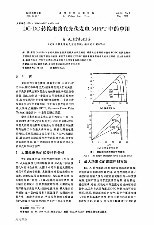
第30卷第3期2008年05月武汉工程大学学报J.WuhanInst.Tech.VoI.30No.3May2008文章编号:1674—2869(2008)03—0104—03DC—DC转换电路在光伏发电MPPT中的应用杨帆,彭宏伟,胡为兵(武汉工程大学电气信息学院,湖北武汉430074)摘要:采用C8051F020单片机控制系统实现最大功率点跟踪,对最大功率跟踪控制中DC-DC转换电路的原理和控制方法进行了研究和实验,采用了升降压式IX;一IX;转换电路来实现最大功率点跟踪,该方法电路简单、软硬件结合、控制方法灵活,明显提高了光伏发电系统的整机效率.关键词:DC—DC转换电路;最大功率点跟踪;光伏发电系统中国分类号:TM464文献标识码;AO引言太阳能作为绿色能源,具有无污染、无噪音、取之不尽、用之不竭等优点,越来越受到人们的关注.由于光伏系统主要问题是电池的转换效率低且价格昂贵,因此,如何进一步提高太阳能电池的转换效率,如何充分利用光伏阵列转换的能量,一直是光伏发电系统研究的主要方向。
太阳链光伏发电系统的最大功率点跟踪(MPPT,MaximumPowerPointTracker)就是其中一个重要的研究课题.最大功率点跟踪是太阳能并网发电中的一项重要的关键技术,它是指为充分利用太阳能,控制改变太阳能电池阵列的输出电压或电流的方法使阵列始终工作在最大功率点上,根据太阳能电池的特性,实现的跟踪方法主要有以下三种:太阳追踪、最大功率点跟踪或两种方法综合使用.出于经济方面的考虑,在小规模的系统中经常使用最大功率点跟踪的方法[1].1太阳能电池的伏安特性分析太阳能电池的输出特性曲线如图1所示,其中(a)为温度变化时的特性曲线,(b)是日照强度变化时的特性曲线.从图l中可以看出太阳能电池具有明显的非线性.太阳能电池的输出受日照强度、电池结温等因素的影响.当结温增加时,太阳能电池的开路电压下降,短路电流稍有增加,最大输出功率减小;当日照强度增加时,太阳能电池的开路电压变化不大,短路电流增加,最大输出功率增加.在一定的温度和日照强度下,太阳能电池具有唯一的最大功率点,当太阳能电池工作在该点时,能输出当前温度和日照条件下的最大功率.UN(a)温度变化时“,V(b)日照强度变化时围1太阳能电池的输出特性曲线Fig.1T.heoutputcharacterofsolararray2最大功率点的跟踪控制方法DC—DC转换电路(也称为斩波电路或斩波器)是接在直流电源和负载之间,通过控制电压将不可控的直流输入变为可控的直流输出的一种变换电路.它被广泛应用于直流开关电源,逆变系统、通信领域、地铁、无轨电车等直流电动机的驱动设备中.从工作方式的角度,DCIDC转换电路可分为升压、降压、升降压和丘克四种,其中升压式和降压式电路是基本的类型,后面二者可以从前面二者派生出来,而降压、升压和升降压式DC.DC转收稿日期:2007一05—25作者简介:杨帆(1966一),女,湖北公安人,教授,硕士.研究方向:智能控制与测试技术.第3期杨帆,等:DC-DC转换电路在光伏发电MPPT中的应用105换电路是比较常用的类型.在实际使用中用DC—DC变换器实现最大功率点跟踪有不同的方法,如,一控制谐振频率的谐振法、控制DC—DC变换器中开关管输入脉冲的占空比等方法.谐振法是利用开.关型电压逆变器的输出电压,通过电感L、电容C产生谐振,L上的电压再通过变压器和桥式整流向蓄电池充电.该方法可以通过改变工作频率来调节输出电压和电流,实现最大功率点跟踪,但线路较复杂,需用中间变压器[2].将DC-DC变换器接入太阳能电池的输入回路,并对DC-DC变换器的输入、输出电压和电流测量结果通过单片机的分析运算,由单片机输出PWM脉冲调节DC-DC转换器内部开关管的占空比来控制太阳能电池的输出电流,从而使蓄电池电压保持恒定。


一、英翻中1、At the end of 2011,cumulative global photovoltaic (PV) installation surpassed 69 GW,an increase of almost 70%,and PV power stations are commonplace in Germany,Italy,and Spain.2011年底全球的光电装机容量已超过690亿W,增长近70%,光电站在德国、意大利、西班牙十分普遍。
2、It can act as a transformer with inherent current limitation due to its lower coupling between the primary and the secondary winding,which is unwanted in most other cases.由于在一次绕组和二次绕组之间有降低的耦合,这种变压器可做限流变压器用,这种功能在大多数其他情况下很少使用。
3、Extra voltage tappings are sometimes included,but to earn the name ‘isolating transformer it is expected that theywill usually be used at 1:1 ratio.有时也包括额外的电压抽头,但人们期望这种变压器的常用变比识1:1,故将其命名为“隔离变压器”。
4、The voltage used is appropriate for the shorter distance and varies from 2300V to about 35000V depending on utility standard practice,distance,and load to be served.他使用的电压适用于较短的距离,其变化为2300~35000V,电压值的大小取决于电力公司操作标准、传输的距离和负荷的大小。

| GIGAFUSE: HIGH VOLTAGE BATTERY FAST DISCONNECTA FAST AND PRECISE CIRCUIT PROTECTION SOLUTION FOR ADVANCED BATTERY SYSTEMS DURING SHORT CIRCUIT AND OVERCURRENT SITUATIONSSPECIFICATIONSUnitsV A MW ms Device Resistance, beginning of life mΩThe high current levels and power densities in advanced battery systems demand equally high-performance safety components. Available in both passive and passive/active (active version production phase available at 3Q2023) combinations, the GigaFuse from GIGAVAC, a brand of Sensata Technologies, is a fast-acting electromechanical device with low heat generation that allows for circuit trips at exact currents and features a design that easily pairs with contactors and eliminates thermal aging fatigue associated with typical DC fuses.FeaturesSensata’s Value• F unctional Safety: Passive technology with electro-mechanical release mechanism • F ast disconnect: <3ms clear time independent from current level • S ystem protection coordination: tunable trip current to easily pair with HV contactors • O ptional active control: to provide designers flexibility of active/passive protection methods (production phase available at 2Q2023)• U p to 10MW interrupt capability • 400A continuous current carry (4/0 busbars); Consult engineering for higher current• W orld-class automotive component supplier • A pplication expertise, significant automotive knowledge base including quality and supply chain • G lobal/Local approach, engineering, and commercial support • S urety of supply: global manufacturing capabilityDIMENSIONSDimensions are in [inches] millimetersTolerance is +/- 0.5mm for all dimensions, unless stated otherwise.MountingM5 or No. 10 ScrewsTorque 1.7 - 4 Nm [15-35in-lb]Case MaterialThermoplastic Polyamide ResinPower ConnectionM8 x 1.25 FemaleTorque 12-18 Nm [106-159 in-lb]Pyro ConnectionTE 411-78033Qualified Acc. to LV 16 and USCARInitiator Resistance: ≥1.7Ω and ≤2.5ΩTriggering Pulse Current: ≥1.75A / 0.5ms≥1.2A / 2.0msDiagnostic Current: ≤100mANo Trigger Current: ≤0.4A or ≤5.0A / 4μsColor of connector retainer may vary due to supplyavailabilitySIDEMOUNTUPRIGHTORDERING OPTIONSMOMENTARY CURRENT CURVE80°C terminal temperature rise at specified curveExample: GFPA415BPassive/Active, 1500A Trip Current, Horizontal Mount OrientationPage 4Sensata Technologies, Inc. (“Sensata”) data sheets are solely intended to assist designers (“Buyers”) who are developing systems that incorporate Sensata products (also referred to herein as “components”). Buyer understands and agrees that Buyer remains responsible for using its independent analysis, valuation, and judgment in designing Buyer’s systems and products. Sensata data sheets have been created using standard laboratory conditions and engineering practices. Sensata has not conducted any testing other than that specifically described in the published documentation for a particular data sheet. Sensata may make corrections, enhancements, improvements, and other changes to its data sheets or components without notice.Buyers are authorized to use Sensata data sheets with the Sensata component(s) identified in each particular data sheet. HOWEVER, NO OTHER LICENSE, EXPRESS OR IMPLIED, BY ESTOPPEL OTHERWISE TO ANY OTHER SENSATA INTELLECTUAL PROPERTY RIGHT, AND NO LICENSE TO ANY THIRD PARTY TECHNOLOGY OR INTELLECTUAL PROPERTY RIGHT, IS GRANTED HEREIN. SENSATA DATA SHEETS ARE PROVIDED “AS IS”. SENSATA MAKES NO WARRANTIES OR REPRESENTATIONS WITH REGARD TO THE DATA SHEETS OR USE OF THE DATA SHEETS, EXPRESS, IMPLIED, OR STATUTORY, INCLUDING ACCURACY OR COMPLETENESS. SENSATA DISCLAIMS ANY WARRANTY OF TITLE AND ANY IMPLIED WARRANTIES OF MERCHANTABILITY, FITNESS FOR A PARTICULAR PURPOSE, QUIET ENJOYMENT, QUIET POSSESSION, AND NON-INFRINGEMENT OF ANY THIRD PARTY INTELLECTUAL PROPERTY RIGHTS WITH REGARD TO SENSATA DATA SHEETS OR USE THEREOF.All products are sold subject to Sensata’s terms and conditions of sale supplied at SENSATA ASSUMES NO LIABILITY FOR APPLICATIONS ASSISTANCE OR THE DESIGN OF BUYERS’ PRODUCTS. BUYER ACKNOWLEDGES AND AGREES THAT IT IS SOLELY RESPONSIBLE FOR COMPLIANCE WITH ALL LEGAL, REGULATORY, AND SAFETY-ELATED REQUIREMENTS CONCERNING ITS PRODUCTS, CONTACT USAmericas+1 (805) 684-8401 *******************GENERAL NOTES1.For customers who can accommodate a vented device, contact Sensata Technologies for more information.2. Current rating (both continuous and momentary) is dependent on bus bar size and customer specific application conditions. Consult with Sensata Technologies for specific details.3. Performance in application will vary based on customer environment and system isolation requirements. Validated at following conditions: 650 V, 15.5kA, 12 µH system inductance. Up to 850 V, 12kA, with 4 µH system inductance. For 1000V application above 3kA, contact Sensata engineering4. Clear time below 5kA can reach up to 4 ms max. IR after 8MW interrupt >1MΩ5. Insulation resistance is dependent on power level of max interrupt load and IR increases with reduced power levels or lower system inductance. IR after standalone short circuit may be below 0.5M at system inductance over 4uH. Performance when tested at system level will show improved IR post interrupt.6. Device can operate in higher ambient temperatures with derated current carry while below maximum terminal temperature.7. Measured on top of the bus bar at the bolted joint. Customer is responsible for ensuring this condition is met otherwise damage to device can occur.8. Sensata Technologies recommends orienting Z axis orthogonal to any mechanical shock pulses to ensure robust performance under load. Sensitivity is dependent on trip setting, consult with Sensata Technologies for more details. See photo for axis orientation.9. Performance depends on specific vibration profile and trip level, consult with Sensata Technologies for your specific requirements. 10. For Automotive Applications please request technical workshop with Sensata Technologies Application Engineering.WARNINGSRISK OF MATERIAL DAMAGE AND HOT ENCLOSURE• The product’s side panels may be hot, allow the product to cool before touching • Follow proper mounting instructions including torque values • Do not allow liquids or foreign objects to enter this productFailure to follow these instructions can result in serious injury, or equipment damage.HAZARD OF ELECTRIC SHOCK, EXPLOSION OR ARC FLASH• Disconnect all power before installing or working with this equipment • Verify all connections and replace all covers before turning on powerFailure to follow these instructions can result in death or serious injury.STRONG MAGNETS PRESENT• This device may present a risk to people with pacemakers if brought within 5 inches (125mm) of device• This device may present a risk to computer drives or other magnetic sensitive electronics or attract small metal tools within 4 inches (100mm) of the device.Failure to follow these instructions can result in death or serious injury.。
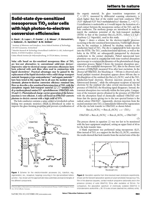
Nature © Macmillan Publishers Ltd 19988Solid-state dye-sensitized mesoporous TiO 2solar cells with high photon-to-electron conversion efficienciesU.Bach *,D.Lupo †‡,P .Comte *,J.E.Moser *,F .Weissortel §,J.Salbeck §,H.Spreitzer †&M.Gratzel **Institute of Photonics and Interfaces,Swiss Federal Institute of Technology,CH-1015Lausanne,Switzerland†Hoechst Research &Technology Deutschland GmbH &Co.KG,Industriepark Ho¨chst,D-65926Frankfurt,Germany §Max-Planck-Institut fu¨r Polymerforschung,D-55128Mainz,Germany .........................................................................................................................Solar cells based on dye-sensitized mesoporous films of TiO 2are low-cost alternatives to conventional solid-state devices 1.Impressive solar-to-electrical energy conversion efficiencies have been achieved with such films when used in conjunction with liquid electrolytes 2.Practical advantages may be gained by the replacement of the liquid electrolyte with a solid charge-transport material.Inorganic p-type semiconductors 3,4and organic materials 5–9have been tested in this regard,but in all cases the incident mono-chromatic photon-to-electron conversion efficiency remained low.Here we describe a dye-sensitized heterojunction of TiO 2with the amorphous organic hole-transport material 2,2Ј,7,7Ј-tetrakis(N ,N -di-p -methoxyphenyl-amine)9,9Ј-spirobifluorene (OMeTAD;refs.10and 11).Photoinduced charge-carrier generation at the hetero-junction is very efficient.A solar cell based on OMeTAD converts photons to electric current with a high yield of 33%.The hole conductor contains a spiro-centre (a tetrahedral carbon linking two aromatic moieties)which is introduced in order to improve the glass-forming properties and prevent crystallization ofthe organic material.Its glass transition temperature of T g ¼120ЊC,measured by differential scanning calorimetry,is much higher then that of the widely used hole conductor TPD (N ,N Ј-diphenyl-N ,N Ј-bis(3-methylphenyl)4,4Ј-diamine;T g ¼62ЊC).Crystallization is undesirable as it would impair the formation of a good contact between the mesoporous surface of the TiO 2and the hole conductor.The methoxy groups are introduced in order to match the oxidation potential of the hole-transport medium (HTM)to that of the sensitizer Ru(II )L 2(SCN)2(where L is 4,4Ј-dicarboxy-2,2Ј-bipyridyl),used in this study.Figure 1shows a scheme for the electron-transfer processes occurring at the dye-sensitized heterojunction.Visible-light absorp-tion by the sensitizer is followed by electron transfer to the conduction band of TiO 2.The dye is regenerated by hole injection into the HTM.The TiO 2conduction-band electrons,as well as the holes in the HTM,are subsequently transported by electronic conduction to the contact electrodes.Pulsed nanosecond laser photolysis was used in conjunction with time-resolved absorption spectroscopy to scrutinize the dynamics of the photoinduced charge separation process.Figure 2shows the transient absorption spec-trum of a dye-sensitized mesoporous TiO 2film in the absence and presence of OMeTAD,measured 50ns after laser excitation.In the absence of OMeTAD,dye bleaching at ϳ500nm is observed and a broad positive transient absorption appears above 600nm due to the absorption of the oxidized dye Ru(III )L 2(SCN)+2and of the TiO 2conduction-band electrons.Electron injection proceeds in the femtosecond domain 12,while the subsequent recapture of injected electrons by the oxidized dye takes several microseconds.In the presence of OMeTAD,the bleaching signal disappears.Instead,the transient absorption rises vertically within the laser par-ison of the transient spectra obtained in the presence of OMeTAD with the absorption band of chemically oxidized OMeTAD con-firms that the species giving rise to the new spectral feature is the radical cation OMeTAD +.Apparently,electron injection from the excited sensitizer into TiO 2is immediately followed by regeneration of the dye via hole transfer to OMeTAD,as shown below:Ru ðII ÞL 2ðSCN Þء2→Ru ðIII ÞL 2ðSCN Þþ2þe ϪðTiO 2Þð1ÞOMeTAD þRu ðIII ÞL 2ðSCN Þþ2→Ru ðII ÞL 2ðSCN Þ2þOMeTADþð2ÞThe process shown in equation (2)was too fast to be monitored with the laser equipment employed,setting an upper limit of 40ns for the hole-transfer time.A blank experiment was performed using mesoporous Al 2O 3films instead of TiO 2as a support for the Ru(II )L 2(SCN)2sensitizer;the results showed that hole transfer from the excited state of the dyeletters to natureNATURE |VOL 395|8OCTOBER 1998|5833OCH 3φ(V)0OMeTAD Figure 1Scheme for the electron-transfer processes (inj.,injection;reg.,regeneration;rec.,recapture;hopping)occurring in the dye-sensitized hetero-junction.Also shown are the approximate redox potentials and band energies of the different components.‡Present address:Materials Science Laboratories,Sony International (Europe)GmbH,Stuttgarter Strasse 106,70736Fellbach,Germany.Wavelength (nm)1050-5-10∆A b s . (10-3)Figure 2Absorption spectra from time-resolved laser photolysis experiments.Shown are the transient absorption spectra of a dye-sensitized mesoporous TiO 2film in the absence (squares,contact medium propylene carbonate)and in the presence (circles)of solid OMeTAD,50ns after excitation at 532nm.Forcomparison,the absorption spectrum of chemically oxidized OMeTAD in chlorobenzene :acetonitrile ¼90:10is also shown (dashed line,arbitrary units).Nature © Macmillan Publishers Ltd 19988to the OMeTAD does not contribute significantly to the photo-induced charge-separation phenomena observed.The photovoltaic performance of the dye-sensitized heterojunc-tion was studied by means of sandwich-type cells,shown schema-tically in Fig.3a.The working electrode consisted of conducting glass (F-doped SnO 2,sheet resistance 10Q per square)onto which a compact TiO 2layer was deposited by spray pyrolysis 13.This avoids direct contact between the HTM layer and the SnO 2which would short-circuit the cell.A 4.2-m-thick mesoporous film of TiO 2was deposited by screen printing onto the compact layer 14,and deriva-tized with Ru(II )L 2(SCN)2by adsorption from acetonitrile.The HTM was introduced into the mesopores by spin-coating a solution of OMeTAD in chlorobenzene onto the TiO 2film,and subsequent evaporation of the solvent.A semi-transparent gold back contact was evaporated on top of the hole conductor under vacuum.Figure 3b shows the photocurrent action spectrum of a typical cell under short-circuit conditions.The given values are not corrected for reflection and absorption losses of the conducting glass,which are estimated to be at least 15%in the visible region of the spectrum.The spectrum closely matches the absorption spectrum of the dye,confirming that the observed photocurrent arises from electron injection by the sensitizer.The maximum value of the incident photo-to-electron conversion efficiency (IPCE)is 33%,which is more than two orders of magnitude larger than the previously reported value for a similar dye-sensitized solid heterojunction 9and only a factor of ϳ2lower than with liquid electrolytes 2.The coating solution used for the device in Fig.3b contained 0.33mM N(PhBr)3SbCl 6and 15mM Li[(CF 3SO 2)2N]in addition to 0.17M OMeTAD.In the absence of these additives,the maximum IPCE was only 5%.N(PhBr)3SbCl 6acts as a dopant,introducing free charge carriers in the HTM by oxidation,as confirmed by spectro-electrochemical measurements.Partial oxidation of OMeTAD by N(PhBr)3SbCl 6is a convenient way to control the dopant level 15.On adding N(PhBr)3SbCl 6to a solution of OMeTAD in chlorobenzene,the radical cation OMeTAD +is instantly formed.The spectral features of OMeTAD +remained unchanged during solvent eva-poration and glass formation,except for a small hypochromic shift.No subsequent absorption changes were detectable over several weeks,confirming the temporal stability of OMeTAD +in the HTM.The second additive,Li[(CF 3SO 2)2N],is a source of Li +ions,which are known to be potential-determining for TiO 2(ref.16).Along with the protons from the carboxylic acid groups of Ru(II )L 2(SCN)2,they confer a positive charge on the surface of the oxide.As the sensitizer is negatively charged a local electrostatic field is produced,assisting electron injection into the TiO 2while retard-ing recapture of the electron by the oxidized dye.The lithium salt may also compensate for space-charge effects.Under light illumina-tion of the heterojunction,a net positive space charge is expected to be formed in the HTM,inducing a local field that impairs current flow.The lithium salt could screen this field,thereby eliminating the space-charge control of the photocurrent.Improvement of the photovoltaic performance of dye-sensitized heterojunctions by immersion in LiClO 4solutions was also reported by Murakoshi et al.5.Figure 4shows current-density/voltage curves employing the device structure shown in Fig.3a.Curves I and II were obtained with hole conductor containing both the N(PhBr)3SbCl 6dopant and the Li[(CF 3SO 3)2N]salt,whereas these additives were absent for curve III.Curve I was measured in the dark,whereas II and III were obtained under light illumination.The device that contains the hole conductor without additives performs poorly,the conversion yield being only 0.04%at a white-light illumination of 9.4mW cm −2.Addition of the dopant and Li +salt increases the overall conversion efficiency to 0.74%.Under full sunlight (100mW cm −2,air mass 1.5),the short-circuit photocurrent density reached 3.18mA cm −2,a value which is unprecedented for solar cells based on organic solids.Further improvement of the photovoltaic performance is expected,as many parameters of the cell assembly have not yet been opti-mized.Preliminary stability tests performed over 80h using the visible output of a 400W Xe lamp showed that the photocurrent was stable within Ϯ20%,while the open-circuit voltage and the fill factor (see Methods)increased.The total charge passed through the cell during illumination was 300C cm −2;corresponding to turnover numbers of about 8,400and 60,000for the OMeTAD and the dye,respectively.This shows that the hole conductor can sustain photo-voltaic operation without significance degradation.From the present findings,the concept of dye-sensitized hetero-junctions emerges as a very interesting and viable option for futureletters to nature584NATURE |VOL 395|8OCTOBER 1998|Wavelength (nm)abI P C E (%)Figure 3Structure and spectral response of the photovoltaic devices.a ,Structure 1,conducting F-doped SnO 2-coated glass;2,compact TiO 2layer;3,dye-sensitized heterojunction;4,gold electrode.b ,Photocurrent action spectrum for a dye-sensitized heterojunction,the structure of which is shown above.The IPCE value corresponds to the number of electrons generated by monochromatic light in the external circuit,divided by the number of incident photons.The 4.2-m-thick mesoporous TiO 2film was sensitized with Ru(II )L 2(SCN)2,spin-coated with a solution of 0.17M OMeTAD,0.33mM N(PhBr)3SbCl 6and 15mM Li[(CF 3SO 2)2N in chlorobenzene with 5%acetonitrile added.0Voltage (V)C u r r e n t d e n s i t y (m A c m –2)Figure 4Current-density/voltage characteristics.Shown are characteristics of the same device as in Fig.3,obtained in the dark (I)and under white-light illumination at 9.4mW cm −2(II).The spectral distribution corresponded to global air mass 1.5corrected for spectral mismatch.The short-circuit current density was 0.32mA cm −2,the open-circuit voltage 342mV and the fill factor 62%corresponding to an overall conversion efficiency of 0.74%.For comparison,the photocurrent-density/voltage characteristic of a cell containing no N(PhBr)3SbCl 6or Li[(CF 3SO 2)2N is also shown (III).Nature © Macmillan Publishers Ltd 19988low-cost solid-state solar cells.Photodiodes based on interpenetrat-ing polymer networks of poly(phenylenevinylene)derivatives 17,18present a related approach.The main difference to our system is that at least one component of the polymer network needs to function simultaneously as an efficient light absorber and a good charge-transport material.The dye-sensitized heterojunction cell offers a greater flexibility,as the light absorber and charge-transport material can be selected independently to obtain optimum solar-energy harvesting and high photovoltaic output.Ⅺ.........................................................................................................................MethodsCompounds.OMeTAD was pure according to 1H-NMR and HPLC analysis.The synthesis will be reported elsewhere.Ru(II )L 2(SCN)2was prepared as previously described 2.Transient absorption spectroscopy.This was carried out with a Nd-YAG laser as excitation light source,producing a 6-ns pulse at 532nm of typically 1mJ cm −2,with a repetition frequency of 30Hz.The probe light was provided by a Xe lamp,which was spectrally narrowed by cut-off and interference filters before passing the device.A monochromator combined with a photomultiplier was used as detection system.A T ektronix 524TDS oscilloscope was used to record and store the data.For the laser experiments,dye-sensitized mesoporous semiconductor films were deposited on ordinary glass.Photocurrent-voltage characteristics.These were measured with a Keithley 2400Source Meter and a 400W Xe lamp.A Schott KG3filter was used in order to approach the spectral distribution of the lamp to air mass 1.5G.The light intensity was regulated to the desired energy output by using a silicon solar cell,calibrated at the ISE-Fraunhofer Institut in Freiburg Germany.Efficiencies were corrected for the spectral mismatch.The fill factor (FF)is defined as FF ¼V opt I opt =I sc V oc ,where V opt and I opt are respectively current and voltage for maximum power output,and I sc and U oc are the short-circuit current and open-circuit voltage,respectively.Received 8May;accepted 13July 1998.1.O’Regan,B.&Gra¨tzel,M.A low-cost,high-efficiency solar cell based on dye-sensitized colloidal TiO 2films.Nature 353,737–739(1991).2.Nazeeruddin,M.K.et al .Conversion of light to electricity by cis-X 2bis(2,2Ј-bipyridyl-4,4Ј-dicarbox-ylate)ruthenium(II)charge-transfer sensitizers (X ¼Cl −,Br −,I −,CN −and SCN −)on nanocrystalline TiO 2electrodes.J.Am.Chem.Soc.115,6382–6390(1993).3.O’Regan,B.&Schwarz,rge enhancement in photocurrent efficiency caused by UVillumination of the dye-sensitized heterojunction TiO 2/RuLL ЈNCS/CuSCN:initiation and potential mechanism.Chem.Mater.10,1501–1509(1998).4.T ennakone,K.,Kumara,G.R.R.A.,Kumarasinghe,A.R.,Wijayantha,K.G.U.&Sirimanne,P .M.Dye-sensitized nano-porous solid-state photovoltaic cell.Semicond.Sci.Technol.10,1689–1693(1995).5.Murakoshi,K.,Kogure,R.&Yanagida,S.Solid state dye-sensitized TiO 2solar cell with polypyrrole ashole transport layer.Chem.Lett.5,471–472(1997).6.Bach,U.et al .Ultrafast hole injection from dye molecules into an organic hole conductor for dyesensitized solid state solar cells.Abstract Book,Bayreuth Polymer &Materials Research Symposium ,P28(Bayreuth,1997).7.Weisso¨rtel, F.Amorphous niedermolekulare Ladungstransportmaterialien fu ¨r nanokristalline Solarzellen.Thesis,Univ.Regensburg (1996).8.Gra¨tzel,M.in Future Generation Photovoltaic Technologies Vol.404(ed.McConnell,R.)119–126(Am.Inst.Phys.,Denver,1997).9.Hagen,J.et al .Novel hybrid solar cells consisting of inorganic nanoparticles and an organic holetransport material.Synth.Met.89,215–220(1997).10.Salbeck,J.,Weisso¨rtel,F.&Bauer,J.Spiro linked compounds for use as active materials in organic light emitting diodes.Macromol.Symp.125,121–132(1997).11.Salbeck,J.,Yu,N.,Bauer,J.,Weisso¨rtel,F.&Bestgen,H.Low molecular organic glasses for blue electroluminescence.Synth.Met.91,209–215(1997).12.Tachibana,Y.,Moser,J.E.,Gra¨tzel,M.,Klug,D.R.&Durrant,J.R.Subpicosecond interfacial charge separation in dye-sensitized nanocrystalline titanium dioxide films.J.Phys.Chem.100,20056–20062(1996).13.Kavan,L.&Gra¨tzel,M.Highly efficient semiconducting TiO 2photoelectrodes prepared by aerosol pyrolysis.Electrochim.Acta 40,643–652(1995).14.Barbe´,C.J.et al .Nanocrystalline titanium oxide electrodes for photovoltaic applications.J.Am.Ceram.Soc.80,3157–3171(1997).15.Abkowitz,M.&Pai,parison of the drift mobility measured under transient and steady-state conditions in a prototypical hopping system.Phil.Mag.B 53,192–216(1986).16.Enright,B.,Redmond,G.&Fitzmaurice,D.Spectroscopic determination of flat-band potentials forpolycrystalline TiO 2electrodes in mixed-solvent systems.J.Phys.Chem.97,1426–1430(1994).17.Halls,J.J.M.et al .Efficient photodiodes from interpenetrating polymer networks.Nature 376,498–500(1995).18.Yu,G.,Gao,J.,Hummelen,J.C.,Wudl,F.&Heeger,A.J.Polymer photovoltaic cells:enhancedefficiencies via a network of internal donor acceptor heterojunctions.Science 270,1789–1791(1995).Acknowledgement.This work was supported by the Swiss National Science Foundation and the European Joule III programme (OFES).Correspondence and requests for materials should be addressed to M.G.(e-mail:michael.graetzel@epfl.ch).letters to natureNATURE |VOL 395|8OCTOBER 1998|585Accumulation of persistent organochlorine compounds in mountains of western CanadaJules M.Blais *†,David W.Schindler *,Derek C.G.Muir †‡,Lynda E.Kimpe §,David B.Donald k &Bruno Rosenberg ¶*Department of Biological Sciences,University of Alberta,Edmonton,Alberta,Canada T6G 2E9‡Department of Fisheries and Oceans,Freshwater Institute,501University Crescent,Winnipeg,Manitoba,Canada R3T 2N6§Public Health Sciences,University of Alberta,Edmonton,Alberta,Canada T6G 2G3k Environment Canada,Room 300Park Plaza,2365Albert Street,Regina,Saskatchewan,Canada S4P 4K1¶Freshwater Institute,Winnipeg,Manitoba,Canada R3T 2N6.........................................................................................................................Persistent,semi-volatile organochlorine compounds,including toxic industrial pollutants and agricultural pesticides,are found everywhere on Earth,including in pristine polar and near-polar locations 1–4.Higher than expected occurrences of these com-pounds in remote regions are the result of long-range transport in the atmosphere,precipitation and ‘cold condensation’—the progressive volatilization in relatively warm locations and sub-sequent condensation in cooler environments 3,4which leads to enhanced concentrations at high latitudes.The upper reaches of high mountains are similar to high-latitude regions in that they too are characterized by relatively low average temperatures,but the accumulation of organochlorine compounds as a function of altitude has not yet been documented.Here we report organo-chlorine deposition in snow from mountain ranges in western Canada that show a 10-to 100-fold increase between 770and 3,100m altitude.In the case of less-volatile compounds,the observed increase by a factor of 10is simply due to a 10-fold increase in snowfall over the altitude range of the sampling sites.In the case of the more-volatile organochlorines,cold-condensa-tion effects further enhance the concentration of these com-pounds with increasing altitude.These findings demonstrate that temperate-zone mountain regions,which tend to receiveT able 1Correlation between organochlorine concentrations in snow and site elevationsCompound Correlation coefficientVapour pressure(Pa).............................................................................................................................................................................␣-HCH0.85*0.1Heptachlorepoxide 0.75*0.1␥-HCH 0.73*0.03Dieldrin0.42*0.016Endosulphan-I 0.76*0.008c-Chlordane 0.42*0.003t-Chlordane 0.340.003p p ЈDDT 0.000.0001.............................................................................................................................................................................PCBs.............................................................................................................................................................................S Dichloro-0.54*0.2(0.008–0.60)S Trichloro-0.53*0.04(0.003–0.022)S Tetrachloro-0.000.006(0.003–0.10)S Pentachloro-0.000.001(0.0003–0.009)S Hexachloro-0.110.0002(7ϫ10Ϫ4Ϫ0:012)S Heptachloro-0.173ϫ10Ϫ4(2:7ϫ10Ϫ5Ϫ0:0015).............................................................................................................................................................................Correlation coefficients (r )are shown for organochlorine concentrations (ng l −1)in snow and site elevation (m.a.s.l.)for the equation conc :¼a e b Elev :,where a and b are fitted constants.Asterisks show significance at P р0:05,for 19degrees of freedom.Sub-cooled liquid vapour pressures are included for pesticides at 20ЊC (ref.21)and PCBs at 25ЊC (ref.22).Published vapour pressures vary considerably,so these values represent mean reported values for all PCBs in that class.Ranges of published vapour pressures for each PCB category are shown in brackets.Only compounds with mean sample concentrations that were ten times higher than blanks were considered.†Present addresses:Department of Biology,University of Ottawa,30Marie Curie Street,PO Box 450Stn.A,Ottawa,Ontario,Canada K1N 6N5(J.M.B.);Environment Canada,867Lakeshore Road,Burlington,Ontario,Canada L7R 4A6(D.C.G.M).。

中国光刻机英语作文范文Lithography, also known as photolithography, is a crucial process in the manufacturing of semiconductors and microchips. It involves the use of a device called a photolithography machine, commonly known as a wafer stepper or a lithography tool, to transfer a pattern onto a substrate, typically a silicon wafer. This pattern is crucial as it determines the layout of the integrated circuits on the wafer, and therefore it plays a critical role in the overall functionality of the microchip.The lithography process begins with the design of the circuit pattern using specialized software. This pattern is then transferred onto a photomask, which is a high-precision quartz plate that contains the circuit pattern in the form of opaque and transparent regions. The photomask is then loadedinto the lithography machine, along with the silicon wafer coated with a light-sensitive material known as photoresist.During operation, the photomask is illuminated with ultraviolet light, and the pattern is projected onto the wafer. The light-sensitive photoresist undergoes a chemical reaction when exposed to the light, and the pattern is transferred onto the wafer. This process is repeated multiple times to create the desired circuit layout on the entire surface of the wafer.The precision and accuracy of the lithography machine are crucial, as any deviation or error in the pattern transfer can result in defective or non-functional microchips. Therefore, lithography machines are equipped with advanced optical systems, high-precision stages, and sophisticated control algorithms to ensure the highest level of accuracy and consistency in the pattern transfer process.In recent years, the semiconductor industry has witnessed a rapid evolution in lithography technology, driven by the demand for smaller and more complex microchips. This has led to the development of new generation lithography machines, such as extreme ultraviolet (EUV) lithography, which use shorter wavelength light sources to achieve even finercircuit patterns.In conclusion, the role of lithography machines in semiconductor manufacturing cannot be overstated. These high-precision, state-of-the-art devices are instrumental in shaping the future of microelectronics, enabling the production of smaller, faster, and more powerful microchips that drive innovation in various industries.。
电⽓英语翻译专业词汇电⽓⼯程词汇voltage 电压current 电流resistance 电阻reactance 电抗impedance 阻抗conductance 电导inductance 电感inductor 电感器capacitance 电容capacitive 电容性的,电容的shunt capacitor 并联电容器shunt 并联series 串联series circuit 串联电路parallel circuit 并联电路conductor 导线voltmeter 电压表ammeter 电流表arc 电弧charge n 电荷v充电,带电,起电discharge v 放电bridge 电桥valve 电⼦管deenergize 断路dielectric 不导电的/绝缘的generator 发电机motor 电动机audion 三极管diode ⼆极管potentiometer 电位器step-up transformer 升压变压器power system 电⼒系统,电⽹transmission line 输电线breaker 断路器relay 继电器demodulator 解调器radiator 散热器ventilation 通风,换⽓,通风装置alternating relay 交流继电器integrated circuit amplifier 集成电路放⼤器transistor amplifier 晶体管放⼤器terminal 端⼦amplifier/magnifier 放⼤器cable n 电缆v架设电缆fuse 保险丝熔断器interface 接⼝amplitude 振幅幅度波幅digital signal 数字信号coupling 耦合intermittent 周期的dislocation 错位malfunction 故障medium 介质screen 屏蔽dampen 阻尼socket 插孔ground plane 接地层three-phasen 三相potential difference 电位差active element 有源元件ideal independent source 理想独⽴电源watt hour meter 感应线圈frequency changer 变频器control switch 控制开关selector switch 选择开关current transformer 电流互感器power transformer 电⼒变压器phase voltage 相电压constant voltage source 恒定电压源alternating current 交流电流inverting 反相out of phase 异相self-inductor ⾃感mutual-inductor 互感ampere 安培coulomb 库仑joule 焦⽿resistor 电阻器charger 充电器semiconductor 半导体absolute value 绝对值operating supply voltage 电源⼯作电压专业词汇Isolator ⼑闸(隔离开关) Susceptance 电纳regulator 稳压器admittance 导纳rectifier 整流器busbar 母线analog signal 模拟信号asynchronism 异步synchronization 同步armature 电枢attenuate 衰减steam-turbine-driven generator ⽓轮发电机turbine generator 涡轮发电机magnetic flux 磁通量oscilloscope ⽰波器oscillator 震荡器multimeter 万⽤表overlay 叠加效果rated power 额定功率power amplifier 功率放⼤器active voltage 有效电压voltage to current converter 电压电流变换器transformer substation变电站regulation 调节degree of compensation补偿度high voltage shunt reactor⾼抗reactive power compensation⽆功补偿three-column transformer三绕组变压器double-column transformer双绕组变压器power-factor 功率因数voltage grade 电压等级no-load current 空载电流impedance 阻抗positive sequence impedance正序阻抗negative sequence impedance 负序阻抗zero sequence impedance零序阻抗susceptance 电纳stator 定⼦high voltage ⾼压fixed series capacitor compensation固定串联电容补偿voltage stability 电压稳定angle stability 功⾓稳定installed capacity 装机容量transformer substation 变电站degree of compensation 补偿度line drop compensation(LDC)线路补偿器circuit theorems 电路定理superposition theorem 叠加定理substitution theorem 替代定理thevenin-Norton Theorem 戴维宁定理electromagnetism 电磁; 电磁学low-frequency amplifier 低频放⼤器low-frequency bypass 低频旁路voltage distortion 交流电压校准器Single Chip Microprocessor(SCM)单⽚机alternating current(AC) 交流/交流电adjustable pressure conveyor 调压输送机allowable load impedance 允许的负载阻抗closed loop control 闭环控制closed loop voltage gain 闭环电压增益closed-loop gain 死循环增益clutch 离合器/联轴器commutator/rectifier 整流器cut off voltage 临界电压cut-in voltage 闭合电压dielectric adj. 不导电的/绝缘的dielectric puncture 击穿electrical durability 电寿命(万次)electromagnetic resonance 电磁感应electromotive force 电动⼒/电动势positive charge 正电荷negative charge 负电荷Automatic Generation Control(AGC) ⾃动发电控制Power System Stabilizator(PSS) 电⼒系统稳定器polyphase 多相(的)iron-loss 铁损armature circuit 电枢电路dynamic response 动态响应time invariant adj.时不变的self-inductor ⾃感mutual-inductor 互感polarity 极性ventilation 通风,换⽓,通风装置interface 接⼝demodulator 解调器balance indicator 交流平衡指⽰器current calibrator 交流电流校准器resistance box 交流电阻箱voltage distortion 交流电压校准器standard resistor 交流标准电阻器low-frequency bypass 低频旁路power pool 联合电⼒系统;联合电⽹electromagnetism 电磁; 电磁学core/shell forme 铁⼼式/壳式potential difference 电位差dual in-line packages 双列直插式组件automatic control system ⾃动控制系统torque motor ⼒矩电动机amplifier using discrete 分离元件放⼤器potentiometer 电位器voltage-current characteristic 伏安特性topology 拓扑termocouple 热电偶exitation 激发;激励;⼲扰air-gap ⽓隙polyphase n.多相adj. 多相的breakdown torque 失步转矩locked-rotor torque ⽌转转矩nominal frequency 额定频率subtransmission ⼆次输电hydro-generation ⽔⼒发电feeder 馈线;馈电电路thermal unit 热⼒机组active power balance 有功功率平衡load-frequency control(LFC)负荷频率控制sychronous condenser 同步调相机tap-changing transformer 可调分接头变压器tap coil 跳闸线圈magnetic air circuit breaker 磁吹断路器automatic generation control (AGC)⾃动发电控制circuit board 电路板direct current(DC)直流电eddy current 涡流corridor 通路induced current 感⽣电流laminated core 叠⽚铁芯left-hand rule 左⼿定则volt-ampere characteristics 伏安特性simulation analysis 仿真分析one machine - infinity bus system 单机⽆穷⼤系统Electrical Machinery电机学Automatic Control Theory⾃动控制理论Electrotechnics Principle of Circuits 电⼯学Electrical Drive and Control电⼒传动与控制brownout 节约⽤电cathode 阴板、负极cation exchanger 阳离⼦交换器circuit breaker 电路断路器circuit diagram 电路图coaxial cable 同轴电缆cooling tower 冷却塔intermediate relay 中间继电器jumper 跳线、跨接lightning arrestor 避雷器installed capacity 装机容量instrument panel 仪表盘instantaneous power 瞬时功率loss of excitation 励磁损失manual reject ⼿动切换overhead line 架空线plant load factor 电⼚负荷因数potential transformer电压互感器overspeed trip 超速跳闸pyod 热电偶safe potential 安全电压shield 屏蔽层single blade switch单⼑开关star connected system星形连接制"Y" static storage 静态存储器station capacity 发电⼚容量step-down transformer降压变压器substation 变电站、⼦站subtransmission ⼆次输电thermal power plant 热⼒发电⼚thumb rule 安培右⼿定则trip 跳闸、断开star connected system星形连接制"Y"A/C adaptor 电源适配器analog to digital 模拟/数字转换ac induced polarization instrument 交流激电仪adjustable pressure conveyor 调压输送机allowable load impedance 允许的负载阻抗charge neutrality 电中性区Charge Termination Voltage 允电端电压/允电端接电压circuit diagram 电路板circuit switching 电路交换closed-loop voltage gain 死循环电压增益connectors 插接器constant voltage modulation 稳压调节current attenuation 电流减衰装置Current by Phase (AMP) 每相电流current limitative range 电流限制范围cut off voltage 临界电压cut-in voltage 闭合电压Discharge Termination Voltage 放电端电压dropout voltage 跌落电压eddy current 涡电流electormagnetic braking sytem 电磁制动系统electric dipole 电偶极⼦electric shielding 电屏蔽Frequency Hopping 跳频input-output control system (IOCS) 输⼊输出控制系统offset voltage 失调电压。
Product DataSeries 9100Computerized Ambient Monitoring Calibration SystemDESCRIPTIONThe Environics® Series 9100 ComputerizedAmbient Monitoring Calibration System is anadvanced microprocessor controlled instrument fordynamic calibration of ambient air analyzers. TheSeries 9100 automatically performs zero, precision,span and multi-point calibrations using NO, NO2,SO2, CO, 03, hydrocarbons and other gases ofinterest. The 9100 exceeds all U.S. EnvironmentalProtection Agency requirements.The Series 9100 consists of a single chassissupporting 2 thermal mass flow controllers, anozone generation module, a mixing zone, a reactionchamber for gas phase titration, and controlelectronics.Commands are entered from the front panel anddisplayed on a backlit 25 line by 80 character liquidcrystal display. The instrument may also beremotely operated using contact closures or anRS-232 serial data interface.The mass flow controllers are calibrated to a NIST(National Institute of Standards and Technology)traceable primary standard. The calibration dataconsists of a comparison of desired versus actualflow over the full dynamic range of the instrumentwith linear interpolation between points. Calibrationdata is stored in non-volatile memory and may beupdated by the user with a suitable standard.The Series 9100 ozone generator is factorycalibrated using a NIST traceable ozone standard.This temperature controlled, ultra-violet (UV) basedozone generator includes a precision photo-opticalfeedback circuit to compensate for lamp agingeffects as well as built-in pressure compensation.The Series 9100 is available in either a standard19” rack mount or bench top configuration.PRODUCT FEATURES AND BENEFITS•25 line by 80 character display permits editingand viewing of an entire 7 day schedule ofcalibration events in worksheet format.•Automatic calculation of dilution and span gasflows based on commanded concentrationeliminates the need for manual computationand allows rapid transition from point to point.•Internally-stored mass flow controller calibrationdata improves accuracy by as much as a factorof ten and simplifies field recalibration.•Internally-stored ozone generator calibrationdata insures linear, repeatable ozonegeneration without photometer control. Ozonegenerator performance exceeds U.S. EPAcriteria for ozone transfer standards.• Ozone generator pressure compensationensures repeatable ozone generation at a flowrate and back pressure other than that at whichit was originally calibrated.SOFTWAREThe Series 9100 has six primary routinesaccessible through "soft" keys, located immediatelybelow their on-screen labels.•Concentration Mode: User enters targetoutput gas concentration (ppm or %) for thespan gas. The actual concentration isdisplayed during mixing.•Flow Mode: User enters target flow rate (cc'sor liters per minute) for the span gas anddilution gas. Actual flow rates are displayedafter mixing is initiated.•Volts Mode: User enters a command voltageto the mass flow controller and the ozonegenerator. The actual voltage is displayedduring operation.•Program Mode: Permits multi-eventprogramming and unattended automaticoperation of the instrument over a seven-dayschedule.•Calibrate Mode: User enters new calibrationdata for each of the 9100's mass flowcontrollers and ozone generator (can bepassword protected).•Maintain Ports: User enters the name of thespan gas in the source cylinder, itsconcentration (ppm) and the port to which thecylinder is connected.69 Industrial Park Road East, Tolland, CT 06084(860) 872-1111 Fax: (860) 870-9333 World Wide Web: E-mail:*******************Copyright 1996 Environics Inc. Printed in USA 4/98。
英文写出光伏工作原理的作文Photovoltaic Effect and the Functionality of Solar Cells.Photovoltaic cells, also known as solar cells, are an integral part of renewable energy systems, converting sunlight into electrical energy. The underlying principle behind their operation is the photovoltaic effect, a phenomenon where certain materials generate an electric current when exposed to light.Understanding the Photovoltaic Effect.The photovoltaic effect originates from the interaction of light with semiconductor materials, such as silicon. When photons of light strike a semiconductor, they can transfer their energy to electrons within the material. This energy boost allows the electrons to overcome the potential barrier of the semiconductor's atomic structure and become free to move.The movement of these free electrons creates anelectric current. This current can be harnessed by connecting the semiconductor to an external circuit, forming a photovoltaic cell.Semiconductor Properties and Band Gap.The band gap of a semiconductor refers to the energy difference between its valence band and conduction band. In the case of silicon, which is commonly used in solar cells, the band gap is 1.1 electron volts (eV).When photons with energy levels equal to or greater than the band gap strike silicon, they excite electrons from the valence band to the conduction band. The energy provided by the photons corresponds to the movement of electrons across this band gap, resulting in the generation of free electrons and the photovoltaic effect.Structure of a Solar Cell.A solar cell typically consists of multiple layers of semiconductor material sandwiched between conductive electrodes. The top layer, exposed to sunlight, has a positive charge, while the bottom layer has a negative charge.When photons interact with the top layer, they generate free electrons and holes (the absence of electrons). These electrons are drawn towards the positive electrode, while the holes migrate to the negative electrode.Circuit and Energy Conversion.The movement of electrons and holes creates an electric current within the solar cell, which flows through an external circuit connected to the electrodes. This current can be used to power devices or feed into an energy grid.The energy conversion efficiency of a solar cell is the percentage of incident sunlight that is converted into electrical energy. The theoretical maximum efficiency of a single-junction silicon solar cell is around 33.1%, knownas the Shockley-Queisser limit.Factors Affecting Solar Cell Efficiency.Multiple factors influence the efficiency of solar cells, including:Spectral response: The absorption of photons by the semiconductor material, which is determined by its optical properties.Charge carrier recombination: The recombination of free electrons with holes, which decreases the efficiency of current generation.Optical losses: Reflections and absorption losses at the solar cell's surface and within the layers.Temperature: Solar cell efficiency decreases with increasing temperature, particularly for silicon-based cells.Applications of Solar Cells.Solar cells are widely used in various applications, including:Grid-connected photovoltaic systems: Large-scale solar farms and rooftop installations that generate electricityfor the grid.Off-grid systems: Powering remote areas, such ascabins and villages, where access to electricity is limited.Portable and consumer electronics: Solar chargers and power banks for mobile devices, laptops, and portable appliances.Advancements and Future Prospects.Research and development efforts continue to enhancethe efficiency and affordability of solar cells. New materials, cell designs, and manufacturing techniques are being explored to improve their performance and reducecosts.In conclusion, the photovoltaic effect forms the basis of solar cell operation, enabling the conversion of sunlight into electricity. Understanding this principle is crucial for harnessing the potential of renewable energy and transitioning towards a more sustainable future. With ongoing advancements in solar cell technology, the role of these devices in the energy landscape is expected to continue to grow.。
TOSHIBA Photocoupler Infrared LED + Photo ICTLP550Degital Logic IsolationLine Receiver Feedback Control Power Supply Control Switching Power Supply Transistor InvertorTLP550 constructs a high emitting diode and a one chip photo diode − transistor.TLP550 has no base connection, and is suitable for application at noisy environmental condition.This unit is 8−lead DIP package.l Isolation voltage: 2500 Vrms (min.)l Switching speed: t pHL, t pLH = 0.5µs (typ.)(R L =1.9 k Ω) l TTL compatiblel UL recognized: UL 1577, file No. E67349Pin Configuration (top view)1 : N.C.2 : Anode3 : Cathode4 : N.C.5 : Emitter6 : Collector7 : N.C.8 : Cathode126354SchematicGND23V CCV O 5 VTOSHIBA 11−10C4 Weight: 0.54 gUnit in mmMaximum Ratings (Ta = 25°C)Characteristic Symbol Rating UnitForward current (Note 1)I F 25 mA Pulse forward current (Note 2)I FP50 mAPeak transient forwardcurrent (Note 3)I FPT 1 AReverse voltageV R5 VL E DDiode power dissipation(Note 4)P D 45 mWOutput current I O 8 mA Peak output current I OP 16 mA Supply voltage V CC -0.5~15 V Output voltageV O-0.5~15 VD e t e c t o rOutput power dissipation(Note 5)P O 100 mWOperating temperature range T opr -55~100 °C Storage temperature range T stg -55~125 °C Lead solder temperature (10s) T sol 260 °C Isolation voltage(AC, 1min., R.H. = 40~60%)(Note 6)BV S2500 Vrms(Note 1) Derate 0.8mA above 70°C.(Note 2) 50% duty cycle, 1ms pulse width. Derate 1.6mA / °C above 70°C. (Note 3) Pulse width 1µs, 300pps.(Note 4) Derate 0.9mW / °C above 70°C. (Note 5) Derate 2mW / °C above 70°C.Electrical Characteristics (Ta = 25°C)Characteristic Symbol Test condition Min. Typ. Max.UnitForward voltage V FI F = 16 mA1.45 1.65 1.85V Forward voltagetemperature coefficient ∆V F /∆Ta I F = 16 mA― -2―mV / °CReverse current I R V R = 5 V ―― 10 µAL E DCapacitance between terminalC T V F = 0, f = 1MHz― 60 ― pF I OH (1)I F = 0 mA, V CC = V O = 5.5 V ― 3 500 nA I OH (2) I F = 0 mA, V CC = V O = 15 V ― ― 5 µA High level outputcurrentI OHI F = 0 mA, V CC = V O = 15 V Ta = 70°C―― 50 µAD e t e c t o rHigh level supply voltageI CCHI F = 0 mA, V CC = 15 V― 0.01 1 µA Ta = 25°C10 30 ― Rank : 019 30 ― Ta = 0~70°C 5 ― ― Current transfer ratioI O / I FI F = 16 mA V CC = 4.5 V V O = 0.4 VRank : 015 ――%Low level output voltageV OL I F = 16 mA, V CC = 4.5 V I O = 1.1 mA(rank 0: I O = 2.4mA)―― 0.4 VIsolation resistance R S R.H. = 40~60%, V = 1kV DC(Note 6)― 1012 ―ΩC o u p l e dCapacitance between input to outputC SV = 0, f = 1MHz ― 0.8 ― pFSwitching Characteristics (Ta = 25°C)Characteristic Symbol Test Condition Min. Typ. Max.UnitI F = 0→ 16 mA, V CC = 5V, R L = 4.1 k Ω― 0.3 0.8Propagation delay time(H → L)t pHL(Note 7)Rank 0: R L = 1.9 k Ω― 0.5 0.8 µsI F = 16→ 0 mA, V CC = 5V, R L = 4.1 k Ω― 1.0 2.0Propagation delay time (L → H)t pLH(Note 7)Rank 0: R L = 1.9 k Ω― 0.6 1.2 µsCommon mode transient immunity at high output levelC MHI F = 0 mA, V CM = 200 V p -pR L = 4.1 k Ω (rank 0: R L = 1.9 k Ω)(Note 8)― 1500 ― V /µs Common mode transient immunity at low output level C MLI F = 16 mA, V CM = 200 V p -pR L = 4.1 k Ω (rank 0: R L = 1.9 k Ω)(Note 8)― -1500 ― V /µs(Note 6) Device considered two -terminal device: Pins 1, 2, 3 and 4 shorted together and pin 5, 6, 7 and 8 shorted together. (Note 7) Switching time test circuit.(Note 8) Common mode transient immunity test circuit.(Note 9) Maximum electrostatic discharge voltage for any pins: 100V (C = 200pF, R = 0)Pulse inputI F monitorI F V O5V 1.5V V OL(I F (I FI FZ O =50Ω CM H =CM L =160 (V) 160 (V) , t f (µs)t f (µs)F o r w a r d c u r r e n t I F (m A )Forward voltage V F (V)I F – V F1.01.2 1.8 F o r w a r d v o l t a g e t e m p e r a t u r e c o e f f i c i e n t ∆V F / ∆T a (m V/ ℃) 0.1-2.2-2.4-2.6-1.40.5 0.3 -2.0-1.8-1.61 3 10 5 ∆V F / ∆Ta – I FForward current I F (mA)30O u t p u t c u r r e n t I O (m A )l O – I FForward current I F (mA)0.10.50.3130 10050 30010 3 5 Ambient temperature Ta (℃)N o r m a l i z e d I O / I FI O / I F – Ta0.60.40.81.21.0H i g h l e v e l o u t p u t c u r r e n t I O H (µA )Ambient temperature Ta (℃)I OH (1) – Ta3001100503105300.61601208040Forward current I F (mA)I O / I F – I FC u r r e n t t r a n s f e r r a t i oI O / I F (%)0.3 1 3 5O u t p u t v o l t a g e V O (V )Forward current I F (mA)V O – I F2016424Load resistance R L (k Ω)t pHL , t pLH – R LP r o p a g a t i o n d e l a y t i m e t p L H , t p H L (µs )3013 1050 1005 Output voltage V O (V) O u tp u t c u r r e n t I O (m A )I O – V O542 3 167· TOSHIBA is continually working to improve the quality and reliability of its products. Nevertheless, semiconductor devices in general can malfunction or fail due to their inherent electrical sensitivity and vulnerability to physical stress. It is the responsibility of the buyer, when utilizing TOSHIBA products, to comply with the standards of safety in making a safe design for the entire system, and to avoid situations in which a malfunction or failure of such TOSHIBA products could cause loss of human life, bodily injury or damage to property.In developing your designs, please ensure that TOSHIBA products are used within specified operating ranges as set forth in the most recent TOSHIBA products specifications. Also, please keep in mind the precautions and conditions set forth in the “Handling Guide for Semiconductor Devices,” or “TOSHIBA Semiconductor Reliability Handbook” etc..· The TOSHIBA products listed in this document are intended for usage in general electronics applications (computer, personal equipment, office equipment, measuring equipment, industrial robotics, domestic appliances, etc.). These TOSHIBA products are neither intended nor warranted for usage in equipment that requires extraordinarily high quality and/or reliability or a malfunction or failure of which may cause loss of human life or bodily injury (“Unintended Usage”). Unintended Usage include atomic energy control instruments, airplane or spaceship instruments, transportation instruments, traffic signal instruments, combustion control instruments, medical instruments, all types of safety devices, etc.. Unintended Usage of TOSHIBA products listed in this document shall be made at the customer’s own risk.· The information contained herein is presented only as a guide for the applications of our products. No responsibility is assumed by TOSHIBA CORPORATION for any infringements of intellectual property or other rights of the third parties which may result from its use. No license is granted by implication or otherwise under any intellectual property or other rights of TOSHIBA CORPORATION or others. · The information contained herein is subject to change without notice000707EAARESTRICTIONS ON PRODUCT USE。