OB2532A Datasheet_CN_佛山照明_111209
- 格式:pdf
- 大小:833.59 KB
- 文档页数:10

No. 89, Xiyuan Rd., Zhongli City, Taoyuan County 320, ProLight PB2D-3JLA-Gx 3W UV Power LED Technical Datasheet Version: 1.02018/11Main Applications‧UV gluing, UV curing, UV marking‧UV drying of printing inks and lacquers ‧Currency inspection‧Forensic analysis -urine, protein stains ‧Leak detection using fluorescent dyes ‧Detects fluorescing minerals and gems ‧Indoor Lighting ‧Outdoor LightingIntroduction‧ProLight PB2D-3JLA-viewing angle 35°Quartz Package, is one of the smallest high power LED footprint available by ProLight Opto, has offered extended solid-state lighting design possibilities. ProLight PB2D-3JLA-viewing angle 35°is designed with ProLight own Patents and using copper leadframe, the best thermal material of the world.‧PB2D-3JLA-viewing angle 35°qualifies as the JEDEC Level 1 MSL sensitivitylevel and suitable for SMD process, Pb_free reflow soldering capability, and full compliance with EU Reduction of Hazardous Substances (RoHS) legislation.Features‧100% foot print compatible with Cree XP-C / XP-E / XP-G‧Best thermal material solution of the world ‧Best Moisture Sensitivity:JEDEC Level 1‧RoHS compliant ‧Quartz Glass Lens ‧View angle 35°Emitter Mechanical DimensionsNotes:1. The cathode side of the device is denoted by the chamfer on the part body.2. Electrical insulation between the case and the board is required. Do not electrically connecteither the anode or cathode to the slug.3. Drawing not to scale.4. All dimensions are in millimeters.5. Unless otherwise indicated, tolerances are ±0.10mm.6. Please do not solder the emitter by manual hand soldering, otherwise it will damage the emitter.7. Please do not use a force of over 0.3kgf impact or pressure on the lens of the LED, otherwiseit will cause a catastrophic failure.*The appearance and specifications of the product may be modified for improvement without notice.2No. 89, Xiyuan Rd., Zhongli City, Taoyuan County 320,Flux Characteristics, T J= 25°CRadiation Pattern ColorPart NumberEmitterRadiometric Power (mW)@700mA Refer @500mAMinimum Typical TypicalLambertian UV-S PB2D-3JLA-GS755930670 UV-M PB2D-3JLA-GM8301030740 UV PB2D-3JLA-G8301030740●ProLight maintains a tolerance of ±10% on flux and power measurements.●Please do not drive at rated current more than 1 second without proper heat sink.ThermalForward Voltage VF(V)Resistance@700mA Refer @500mA Junction to Color Min.Typ.Max.Typ.Slug (°C/ W) UV-S 3.4 3.7 4.0 3.68UV-M 3.2 3.5 4.0 3.48UV 3.2 3.5 4.0 3.48●ProLight maintains a tolerance of ±0.1V for Voltage measurements.Electrical Characteristics, T J= 25°COptical Characteristics at 700mA, T J= 25°CTotalincluded ViewingAngle AngleRadiationColor Peak Wavelength λP(degrees)(degrees)Pattern Min.Typ.Max.θ0.90V 2 θ1/2Lambertian UV-S365 nm367.5 nm370 nm6035 UV-M385 nm387.5 nm390 nm6035 UV390 nm395 nm400 nm6035●ProLight maintains a tolerance of ±3nm for dominant wavelength measurements.No. 89, Xiyuan Rd., Zhongli City, Taoyuan County 320,3Color Bin CodeMinimum Maximum Available Radiometric Power (mW)Radiometric Power (mW)Color BinsUV-S T2755830All U1830910【1】U29101000【1】V110001100【1】UV-M U1830910All U29101000【1】V110001100【1】V211001210【1】W112101330【1】UV U1830910All U29101000【1】V110001100【1】V211001210【1】W112101330【1】●ProLight maintains a tolerance of ±10% on flux and power measurements.●The flux bin of the product may be modified for improvement without notice.●【1】The rest of color bins are not 100% ready for order currently. Please ask for quote and order possibility.Parameter UV-S/UV-M/UVDC Forward Current (mA)1000Peak Pulsed Forward Current (mA)1100 (less than 1/10 duty cycle@1KHz)ESD Sensitivity±4000V(HBM per MIL-STD-883E Method 3015.7)LED Junction Temperature125°COperating Board Temperature-40°C -85°Cat Maximum DC Forward CurrentStorage Temperature-40°C -100°CSoldering Temperature JEDEC 020c 260°CAllowable Reflow Cycles3Reverse Voltage Not designed to be driven in reverse bias Radiometric Power Bin Structure at 700mAAbsolute Maximum Ratings4No. 89, Xiyuan Rd., Zhongli City, Taoyuan County 320,Color Bin CodeMinimum Peak Maximum Peak Wavelength (nm)Wavelength (nm)UV-S2365370 UV-M A385390UV 1390395 2395400●ProLight maintains a tolerance of ±3nm for peak wavelength measurements.Peak Wavelength Bin StructureForward Voltage Bin StructureColor Bin Code Minimum Voltage (V)Maximum Voltage (V)UV-S E 3.4 3.6F 3.6 3.8G 3.8 4.0UV-M D 3.2 3.4E 3.4 3.6F 3.6 3.8G 3.8 4.0UV D 3.2 3.4E 3.4 3.6F 3.6 3.8G 3.8 4.0●ProLight maintains a tolerance of ±0.1V for Voltage measurements.Note: Although several bins are outlined, product availability in a particular bin varies by production run and by product performance. Not all bins are available in all colors.No. 89, Xiyuan Rd., Zhongli City, Taoyuan County 320,5No. 89, Xiyuan Rd., Zhongli City, Taoyuan County 320, 1. UV-S, UV-M, UV020406080100120140160020406080100120R e l a t i v e L i g h t O u t p u t (%)Junction Temperature, T J (℃)UV-S, UV-M, UV6Color Spectrum, T J = 25°CLight Output CharacteristicsRelative Light Output vs. Junction Temperature at 700mA0.00.20.40.60.81.0250300350400450500550600R e l a t i v e S p e c t r a l P o w e r D i s t r i b u t i o nWavelength (nm)UV-S UV-M UVNo. 89, Xiyuan Rd., Zhongli City, Taoyuan County 320, 0200400600800100012002535455565758595105115125135F o r w a r d C u r r e n t (m A )Solder Temperature (Slug)0.00.20.40.60.81.01.20100200300400500600700800R e l a t i v e R a d i o m e t r i c P o w e rForward Current (mA)10020030040050060070080000.51 1.52 2.53 3.54 4.5A v e r a g e F o r w a r d C u r r e n t (m A )Forward Voltage (V)UV-S, UV-M, UVUV-S, UV-M, UVSolder Temperature (Slug) vs. Maximum Forward CurrentForward Current Characteristics, T J = 25°CFig 1. Forward Current vs. ForwardVoltage for UV-S, UV-M, UV.Fig 2. Relative Radiometric Power vs.Forward Current for UV-S, UV-M, UV at T J =25 maintained.71. UV-S, UV-M, UV (T JMAX = 125°C)No. 89, Xiyuan Rd., Zhongli City, Taoyuan County 320, 0102030405060708090100-100-80-60-40-20020406080100R e l a t i v e I n t e n s i t y (%)Angular Displacement (Degrees)8Typical Representative Spatial Radiation PatternRadiation PatternSoak RequirementsLevel Floor Life Standard Accelerated Environment Time Conditions Time (hours)Conditions Time (hours)Conditions1Unlimited≤30°C /168 +5/-085°C /NA NA 85% RH85% RH●The standard soak time includes a default value of 24 hours for semiconductor manufature'sexposure time (MET) between bake and bag and includes the maximum time allowed out ofthe bag at the distributor's facility.●Table below presents the moisture sensitivity level definitions per IPC/JEDEC's J-STD-020C.Soak Requirements Level Floor Life Standard Accelerated Environment Time Conditions Time (hours)Conditions Time (hours)Conditions1Unlimited≤30°C /168 +5/-085°C /NA NA 85% RH85% RH2 1 year≤30°C /168 +5/-085°C /NA NA 60% RH60% RH2a 4 weeks≤30°C /696 +5/-030°C /120 +1/-060°C / 60% RH60% RH60% RH3168 hours≤30°C /192 +5/-030°C /40 +1/-060°C / 60% RH60% RH60% RH472 hours≤30°C /96 +2/-030°C /20 +0.5/-060°C / 60% RH60% RH60% RH548 hours≤30°C /72 +2/-030°C /15 +0.5/-060°C / 60% RH60% RH60% RH5a24 hours≤30°C /48 +2/-030°C /10 +0.5/-060°C / 60% RH60% RH60% RH6Time on Label≤30°C / Time on Label30°C /NA NA (TOL)60% RH(TOL)60% RHMoisture Sensitivity Level -JEDEC Level 1No. 89, Xiyuan Rd., Zhongli City, Taoyuan County 320,9No. 89, Xiyuan Rd., Zhongli City, Taoyuan County 320, Stress TestStress Conditions Stress Duration Failure CriteriaRoom Temperature 25°C, I F = max DC (Note 1)1000 hours Note 2Operating Life (RTOL)High Temperature 100°C, non-operating 1000 hours Note 2Storage Life (HTSL)Low Temperature -40°C, non-operating 1000 hours Note 2Storage Life (LTSL)Non-operating-40°C to 100°C, 30 min. dwell,200 cyclesNote 2Temperature Cycle (TMCL)<5 min. transferMechanical Shock 1500 G, 0.5 msec. pulse, Note 35 shocks each 6 axis Natural Drop On concrete from 1.2 m, 3X Note 3Variable Vibration10-2000-10 Hz, log or linear sweep rate,Note 3Frequency20 G about 1 min., 1.5 mm, 3X/axisSolder Heat Resistance260°C ±5°C, 10 sec.Note 3(SHR)SolderabilitySteam age for 16 hrs., then solder dipSolder coverageat 260°C for 5 sec.on leadNotes:1. Depending on the maximum derating curve.2. Criteria for judging failureItemTest Condition Criteria for Judgement Min.Max.Forward Voltage (V F )I F = max DC --Initial Level x 1.1Luminous Flux or I F = max DCInitial Level x 0.7--Radiometric Power (ΦV )* The test is performed after the LED is cooled down to the room temperature.3. A failure is an LED that is open or shorted.10Qualification Reliability TestingNo. 89, Xiyuan Rd., Zhongli City, Taoyuan County 320, TYPE A.11Recommended Solder Pad DesignStandard Emitter ●All dimensions are in millimeters.●Electrical isolation is required between Slug and Solder Pad.TYPE B.No. 89, Xiyuan Rd., Zhongli City, Taoyuan County 320, 12Reflow Soldering ConditionProfile FeatureSn-Pb Eutectic Assembly Pb-Free Assembly Average Ramp-Up Rate 3°C / second max.3°C / second max.(T Smax to T P )Preheat–Temperature Min (T Smin )100°C 150°C –Temperature Max (T Smax )150°C 200°C –Time (t Smin to t Smax )60-120 seconds 60-180 seconds Time maintained above:–Temperature (T L )183°C 217°C –Time (t L )60-150 seconds60-150 secondsPeak/Classification Temperature (T P )240°C 260°C Time Within 5°C of Actual Peak 10-30 seconds 20-40 seconds Temperature (t P )Ramp-Down Rate6°C/second max.6°C/second max.Time 25°C to Peak Temperature6 minutes max.8 minutes max.●We recommend using the M705-S101-S4 solder paste from SMIC (Senju Metal Industry Co., Ltd.) for lead-free soldering.●Do not use solder pastes with post reflow flux residue>47%. (58Bi-42Sn eutectic alloy, etc) This kind of solder pastes may cause a reliability problem to LED.●All temperatures refer to topside of the package, measured on the package body surface.●Repairing should not be done after the LEDs have been soldered. When repairing is unavoidable, a double-head soldering iron should be used. It should be confirmed beforehand whether the characteristics of the LEDs will or will not be damaged by repairing.●Reflow soldering should not be done more than three times.●When soldering, do not put stress on the LEDs during heating.●After soldering, do not warp the circuit board.t 25°C to Peakt S PreheatTimeT e m p e r a t u r eCritical Zone T L to T PRamp-upRamp-downT SmaxT Smint Pt LT PT L25IPC-020cNotes:1. Drawing not to scale.2. All dimensions are in millimeters.3. Unless otherwise indicated, tolerances are ±0.10mm.13 No. 89, Xiyuan Rd., Zhongli City, Taoyuan County 320,No. 89, Xiyuan Rd., Zhongli City, Taoyuan County 320, 14Notes:1. Empty component pockets sealed with top cover tape.2. 250, 500 pieces per reel.3. Drawing not to scale.4. All dimensions are in millimeters.178 ± 13 ± 0.54 ± 0.5 5 ± 0.560 ± 0.513.2 ± 0.516.2 ± 0.5Φ 13.1 ± 0.5Φ 21 ± 0.5No. 89, Xiyuan Rd., Zhongli City, Taoyuan County 320, Use Handling of Quartz Lens LEDsNotes for handling of quartz lens LEDs●Please do not use a force of over 3.0kgf impact or pressure on the quartz lens,otherwise it will cause a catastrophic failure.●The LEDs should only be picked up by making contact with the sides of the LED body.●Avoid touching the quartz lens especially by sharp tools such as Tweezers.●Avoid leaving fingerprints on the quartz lens.●Please store the LEDs away from dusty areas or seal the product against dust.●When populating boards in SMT production, there are basically no restrictions regarding the form of the pick and place nozzle, except that mechanical pressure on the quartz lens must be prevented.●Please do not mold over the quartz lens with another resin. (epoxy, urethane, etc)15Precaution for Use●StoragePlease do not open the moisture barrier bag (MBB) more than one week. This may cause the leads of LED discoloration. We recommend storing ProLight’s LEDs in a dry box after opening the MBB. The recommended storage conditions are temperature 5 to 30°C and humidity less than 40% RH. It is also recommended to return the LEDs to the MBB and to reseal the MBB.●The slug is is not electrically neutral. Therefore, we recommend to isolate the heat sink.●We recommend using the M705-S101-S4 solder paste from SMIC (Senju Metal Industry Co., Ltd.) for lead-free soldering.●Do not use solder pastes with post reflow flux residue>47%. (58Bi-42Sn eutectic alloy, etc) This kind of solder pastes may cause a reliability problem to LED.●Any mechanical force or any excess vibration shall not be accepted to apply during cooling process to normal temperature after soldering.●Please avoid rapid cooling after soldering.●Components should not be mounted on warped direction of PCB.●Repairing should not be done after the LEDs have been soldered. When repairing is unavoidable,a heat plate should be used. It should be confirmed beforehand whether the characteristics of the LEDs will or will not be damaged by repairing.●This device should not be used in any type of fluid such as water, oil, organic solvent and etc.When cleaning is required, isopropyl alcohol should be used.●When the LEDs are illuminating, operating current should be decide after considering the package maximum temperature.●The appearance, specifications and flux bin of the product may be modified for improvement without notice. Please refer to the below website for the latest datasheets./。
DATA SHEET General PurposeTransistorsNPN Silicon2N3903, 2N3904Features•Pb−Free Packages are Available*MAXIMUM RATINGSRating Symbol Value UnitCollector−Emitter Voltage V CEO40VdcCollector−Base Voltage V CBO60VdcEmitter−Base Voltage V EBO 6.0VdcCollector Current − Continuous I C200mAdcTotal Device Dissipation @ T A = 25°CDerate above 25°C P D6255.0mWmW/°CTotal Device Dissipation@ T C = 25°C Derate above 25°C P D1.512WmW/°COperating and Storage Junction Temperature Range T J, T stg−55 to +150°CTHERMAL CHARACTERISTICS (Note 1)Characteristic Symbol Max Unit Thermal Resistance, Junction−to−Ambient R q JA200°C/W Thermal Resistance, Junction−to−Case R q JC83.3°C/W Stresses exceeding those listed in the Maximum Ratings table may damage the device. If any of these limits are exceeded, device functionality should not be assumed, damage may occur and reliability may be affected.1.Indicates Data in addition to JEDEC Requirements.*For additional information on our Pb−Free strategy and soldering details, please download the onsemi Soldering and Mounting T echniques Reference Manual, SOLDERRM/D.MARKING DIAGRAMSSee detailed ordering and shipping information in the package dimensions section on page 3 of this data sheet.ORDERING INFORMATIONCOLLECTOR21EMITTER2N390xYWW GGx= 3 or 4Y= YearWW= Work WeekG= Pb−Free Package(Note: Microdot may be in either location)BENT LEADTAPE & REELAMMO PACKSTRAIGHT LEADBULK PACKTO−92CASE 29STYLE 1ELECTRICAL CHARACTERISTICS (T A = 25°C unless otherwise noted)Characteristic Symbol Min Max Unit OFF CHARACTERISTICSCollector−Emitter Breakdown Voltage (Note 2)(I C = 1.0 mAdc, I B = 0)V(BR)CEO40−Vdc Collector−Base Breakdown Voltage (I C = 10 m Adc, I E = 0)V(BR)CBO60−Vdc Emitter−Base Breakdown Voltage (I E = 10 m Adc, I C = 0)V(BR)EBO 6.0−Vdc Base Cutoff Current (V CE = 30 Vdc, V EB = 3.0 Vdc)I BL−50nAdc Collector Cutoff Current (V CE = 30 Vdc, V EB = 3.0 Vdc)I CEX−50nAdc ON CHARACTERISTICSDC Current Gain (Note 2)(I C = 0.1 mAdc, V CE = 1.0 Vdc)2N39032N3904 (I C = 1.0 mAdc, V CE = 1.0 Vdc)2N39032N3904 (I C = 10 mAdc, V CE = 1.0 Vdc)2N39032N3904 (I C = 50 mAdc, V CE = 1.0 Vdc)2N39032N3904 (I C = 100 mAdc, V CE = 1.0 Vdc)2N39032N3904h FE204035705010030601530−−−−150300−−−−−Collector−Emitter Saturation Voltage (Note 2) (I C = 10 mAdc, I B = 1.0 mAdc)(I C = 50 mAdc, I B = 5.0 mAdc V CE(sat)−−0.20.3VdcBase−Emitter Saturation Voltage (Note 2) (I C = 10 mAdc, I B = 1.0 mAdc)(I C = 50 mAdc, I B = 5.0 mAdc)V BE(sat)0.65−0.850.95VdcSMALL−SIGNAL CHARACTERISTICSCurrent−Gain − Bandwidth Product(I C = 10 mAdc, V CE = 20 Vdc, f = 100 MHz)2N39032N3904f T250300−−MHzOutput Capacitance (V CB = 5.0 Vdc, I E = 0, f = 1.0 MHz)C obo− 4.0pF Input Capacitance (V EB = 0.5 Vdc, I C = 0, f = 1.0 MHz)C ibo−8.0pFInput Impedance(I C = 1.0 mAdc, V CE = 10 Vdc, f = 1.0 kHz)2N39032N3904h ie1.01.08.010k WVoltage Feedback Ratio(I C = 1.0 mAdc, V CE = 10 Vdc, f = 1.0 kHz)2N39032N3904h re0.10.55.08.0X 10−4Small−Signal Current Gain(I C = 1.0 mAdc, V CE = 10 Vdc, f = 1.0 kHz)2N39032N3904h fe50100200400−Output Admittance (I C = 1.0 mAdc, V CE = 10 Vdc, f = 1.0 kHz)h oe 1.040m mhosNoise Figure(I C = 100 m Adc, V CE = 5.0 Vdc, R S = 1.0 k W, f = 1.0 kHz)2N39032N3904NF−−6.05.0dBSWITCHING CHARACTERISTICSDelay Time(VCC = 3.0 Vdc, V BE = 0.5 Vdc,I C = 10 mAdc, I B1 = 1.0 mAdc)t d−35nsRise Time t r−35nsStorage Time(V CC = 3.0 Vdc, I C = 10 mAdc,2N3903I B1 = I B2 = 1.0 mAdc)2N3904t s−−175200nsFall Time t f−50ns 2.Pulse Test: Pulse Width v 300 m s; Duty Cycle v 2%.ORDERING INFORMATIONDevicePackage Shipping †2N3903RLRM TO −922000 / Ammo Pack 2N3904TO −925000 Units / Bulk 2N3904G TO −92(Pb −Free)5000 Units / Bulk 2N3904RLRA TO −922000 / Tape & Reel 2N3904RLRAG TO −92(Pb −Free)2000 / Tape & Reel 2N3904RLRM TO −922000 / Ammo Pack 2N3904RLRMG TO −92(Pb −Free)2000 / Ammo Pack 2N3904RLRPTO −922000 / Ammo Pack 2N3904RLRPG TO −92(Pb −Free)2000 / Ammo Pack 2N3904RL1G TO −92(Pb−Free)2000 / Tape & Reel 2N3904ZL1TO −922000 / Ammo Pack 2N3904ZL1GTO −92(Pb −Free)2000 / Ammo Pack†For information on tape and reel specifications, including part orientation and tape sizes, please refer to our Tape and Reel Packaging Specifications Brochure, BRD8011/D.Figure 1. Delay and Rise Time Equivalent Test CircuitFigure 2. Storage and Fall Time Equivalent Test Circuit10 < t 1 < 500 m * T otal shunt capacitance of test jig and connectors* T otal shunt capacitance of test jig and connectorsTYPICAL TRANSIENT CHARACTERISTICSFigure 3. CapacitanceREVERSE BIAS VOLTAGE (VOLTS)2.03.05.07.0101.00.1Figure 4. Charge DataI C , COLLECTOR CURRENT (mA)50001.0Q , C H A R G E (p C )3000200010005003002007001005070 2.0 3.0 5.07.01020305070100200C A P A C I T A N C E (p F )1.02.03.0 5.07.010200.20.30.50.7T J = 25°C T J = 125°CFigure 5. Turn −On TimeI C , COLLECTOR CURRENT (mA)7010020030050050Figure 6. Rise TimeI C , COLLECTOR CURRENT (mA)T I M E (n s )5t , R I S E T I M E (n s )Figure 7. Storage Time I C , COLLECTOR CURRENT (mA)Figure 8. Fall TimeI C , COLLECTOR CURRENT (mA)1030720701002003005005051030720701002003005005051030720701002003005005051030720r t , F A L L T I M E (n s )f t , S T O R A G E T I M E (n s )s ′TYPICAL AUDIO SMALL −SIGNAL CHARACTERISTICSNOISE FIGURE VARIATIONS(V CE = 5.0 Vdc, T A = 25°C, Bandwidth = 1.0 Hz)Figure 9. f, FREQUENCY (kHz)46810122Figure 10.R S , SOURCE RESISTANCE (k OHMS)0N F , N O I S E F I G U R E (d B )04681012214N F , N O I S E F I G U R E (d B )Figure 11. Current GainI C , COLLECTOR CURRENT (mA)7010020030050Figure 12. Output AdmittanceI C , COLLECTOR CURRENT (mA)h , C U R R E N T G A I Nh , O U T P U T A D M I T T A N C E ( m h o s )Figure 13. Input Impedance I C , COLLECTOR CURRENT (mA)Figure 14. Voltage Feedback RatioI C , COLLECTOR CURRENT (mA)3010050510202.03.05.07.0101.00.10.21.02.0 5.00.5100.30.5 3.00.72.05.010201.00.20.5o e h , V O L T A G E F E E D B A C K R A T I O (X 10 )r e h , I N P U T I M P E D A N C E (k O H M S )ie 0.10.21.02.0 5.0100.30.5 3.00.10.21.02.0 5.0100.30.5 3.0210.10.21.02.0 5.0100.30.5 3.0f e m -4h PARAMETERS(V CE = 10 Vdc, f = 1.0 kHz, T A = 25°C)TYPICAL STATIC CHARACTERISTICSFigure 15. DC Current GainI C , COLLECTOR CURRENT (mA)0.30.50.71.02.00.2h , D C C U R R E N T G A I N (N O R M A L I Z E D )0.1F EFigure 16. Collector Saturation RegionI B , BASE CURRENT (mA)0.40.60.81.00.2V , C O L L E C T O R E M I T T E R V O L T A G E (V O L T S )0CE Figure 17. “ON” Voltages I C , COLLECTOR CURRENT (mA)0.40.60.81.01.20.2Figure 18. Temperature CoefficientsI C , COLLECTOR CURRENT (mA)V , V O L T A G E (V O L T S )- 0.500.51.0C O E F F I C I E N T (m V / C )- 1.0- 1.5- 2.0°TO−92 (TO−226)CASE 29−11ISSUE AMDATE 09 MAR 2007STYLES ON PAGE 2NOTES:1.DIMENSIONING AND TOLERANCING PER ANSIY14.5M, 1982.2.CONTROLLING DIMENSION: INCH.3.CONTOUR OF PACKAGE BEYOND DIMENSION RIS UNCONTROLLED.4.LEAD DIMENSION IS UNCONTROLLED IN P ANDBEYOND DIMENSION K MINIMUM.SECTION X−XPLANE DIM MIN MAX MIN MAXMILLIMETERSINCHESA0.1750.205 4.45 5.20B0.1700.210 4.32 5.33C0.1250.165 3.18 4.19D0.0160.0210.4070.533G0.0450.055 1.15 1.39H0.0950.105 2.42 2.66J0.0150.0200.390.50K0.500---12.70---L0.250--- 6.35---N0.0800.105 2.04 2.66P---0.100--- 2.54R0.115--- 2.93---V0.135--- 3.43---BENT LEADTAPE & REELAMMO PACKSTRAIGHT LEADBULK PACKNOTES:1.DIMENSIONING AND TOLERANCING PERASME Y14.5M, 1994.2.CONTROLLING DIMENSION: MILLIMETERS.3.CONTOUR OF PACKAGE BEYONDDIMENSION R IS UNCONTROLLED.4.LEAD DIMENSION IS UNCONTROLLED IN PAND BEYOND DIMENSION K MINIMUM.SECTION X−XDIM MIN MAXMILLIMETERSA 4.45 5.20B 4.32 5.33C 3.18 4.19D0.400.54G 2.40 2.80J0.390.50K12.70---N 2.04 2.66P 1.50 4.00R 2.93---V 3.43---STRAIGHT LEADBULK PACKBENT LEADTAPE & REELAMMO PACKMECHANICAL CASE OUTLINEPACKAGE DIMENSIONSTO−92 (TO−226)CASE 29−11ISSUE AMDATE 09 MAR 2007STYLE 1:PIN 1.EMITTER2.BASE3.COLLECTORSTYLE 6:PIN 1.GATE2.SOURCE & SUBSTRATE3.DRAINSTYLE 11:PIN 1.ANODE2.CATHODE & ANODE3.CATHODESTYLE 16:PIN 1.ANODE2.GATE3.CATHODESTYLE 21:PIN 1.COLLECTOR2.EMITTER3.BASESTYLE 26:PIN 1.V CC2.GROUND 23.OUTPUTSTYLE 31:PIN 1.GATE2.DRAIN3.SOURCE STYLE 2:PIN 1.BASE2.EMITTER3.COLLECTORSTYLE 7:PIN 1.SOURCE2.DRAIN3.GATESTYLE 12:PIN 1.MAIN TERMINAL 12.GATE3.MAIN TERMINAL 2STYLE 17:PIN 1.COLLECTOR2.BASE3.EMITTERSTYLE 22:PIN 1.SOURCE2.GATE3.DRAINSTYLE 27:PIN 1.MT2.SUBSTRATE3.MTSTYLE 32:PIN 1.BASE2.COLLECTOR3.EMITTERSTYLE 3:PIN 1.ANODE2.ANODE3.CATHODESTYLE 8:PIN 1.DRAIN2.GATE3.SOURCE & SUBSTRATESTYLE 13:PIN 1.ANODE 12.GATE3.CATHODE 2STYLE 18:PIN 1.ANODE2.CATHODE3.NOT CONNECTEDSTYLE 23:PIN 1.GATE2.SOURCE3.DRAINSTYLE 28:PIN 1.CATHODE2.ANODE3.GATESTYLE 33:PIN 1.RETURN2.INPUT3.OUTPUTSTYLE 4:PIN 1.CATHODE2.CATHODE3.ANODESTYLE 9:PIN 1.BASE 12.EMITTER3.BASE 2STYLE 14:PIN 1.EMITTER2.COLLECTOR3.BASESTYLE 19:PIN 1.GATE2.ANODE3.CATHODESTYLE 24:PIN 1.EMITTER2.COLLECTOR/ANODE3.CATHODESTYLE 29:PIN 1.NOT CONNECTED2.ANODE3.CATHODESTYLE 34:PIN 1.INPUT2.GROUND3.LOGICSTYLE 5:PIN 1.DRAIN2.SOURCE3.GATESTYLE 10:PIN 1.CATHODE2.GATE3.ANODESTYLE 15:PIN 1.ANODE 12.CATHODE3.ANODE 2STYLE 20:PIN 1.NOT CONNECTED2.CATHODE3.ANODESTYLE 25:PIN 1.MT 12.GATE3.MT 2STYLE 30:PIN 1.DRAIN2.GATE3.SOURCESTYLE 35:PIN 1.GATE2.COLLECTOR3.EMITTERON Semiconductor and are registered trademarks of Semiconductor Components Industries, LLC (SCILLC). SCILLC reserves the right to make changes without further notice to any products herein. SCILLC makes no warranty, representation or guarantee regarding the suitability of its products for any particular purpose, nor does SCILLC assume any liability arising out of the application or use of any product or circuit, and specifically disclaims any and all liability, including without limitation special, consequential or incidental damages.“Typical” parameters which may be provided in SCILLC data sheets and/or specifications can and do vary in different applications and actual performance may vary over time. All operating parameters, including “Typicals” must be validated for each customer application by customer’s technical experts. SCILLC does not convey any license under its patent rights nor the rights of others. SCILLC products are not designed, intended, or authorized for use as components in systems intended for surgical implant into the body, or other applications intended to support or sustain life, or for any other application in which the failure of the SCILLC product could create a situation where personal injury or death may occur. Should Buyer purchase or use SCILLC products for any such unintended or unauthorized application, Buyer shall indemnify and hold SCILLC and its officers, employees, subsidiaries, affiliates, and distributors harmless against all claims, costs, damages, and expenses, and reasonable attorney fees arising out of, directly or indirectly, any claim of personal injury or deathassociated with such unintended or unauthorized use, even if such claim alleges that SCILLC was negligent regarding the design or manufacture of the part. SCILLC is an EqualPUBLICATION ORDERING INFORMATIONTECHNICAL SUPPORTNorth American Technical Support:LITERATURE FULFILLMENT :Email Requests to:*******************Europe, Middle East and Africa Technical Support:。
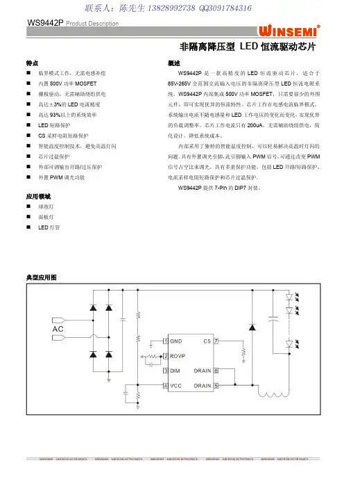
特点⏹临界模式工作,无需电感补偿⏹内置500V 功率MOSFET ⏹栅极驱动,无需辅助绕组供电⏹高达±3%的LED 电流精度⏹高达93%以上的系统效率⏹LED 短路保护⏹CS 采样电阻短路保护⏹智能温度控制技术,避免高温灯闪⏹芯片过温保护⏹外部可调输出开路/过压保护⏹外置PWM 调光功能应用领域⏹球泡灯⏹面板灯⏹LED 灯管概述WS9442P 是一款高精度的LED 恒流驱动芯片,适合于85V-265V 全范围交流输入电压的非隔离降压型LED 恒流电源系统。
WS9442P 内部集成500V 功率MOSFET ,只需要很少的外围元件,即可实现优异的恒流特性。
芯片工作在电感电流临界模式,系统输出电流不随电感量和LED 工作电压的变化而变化,实现优异的负载调整率。
芯片工作电流只有200uA ,无需辅助绕组供电,简化设计,降低系统成本。
内部采用了独特的智能温度控制,可以轻易解决高温时灯闪的问题。
具有外置调光引脚,此引脚输入PWM 信号,可通过改变PWM 信号占空比来调光。
具有多重保护功能,包括LED 开路/短路保护、电流采样电阻短路保护和芯片过温保护。
WS9442P 提供7-Pin 的DIP7封装。
典型应用图非隔离降压型LED 恒流驱动芯片引脚定义与器件标识WS9442P 提供了7-Pin 的DIP-7封装,顶层如下图所示:引脚功能说明电路内部结构框图引脚名引脚号功能说明1GND 芯片地2ROVP 输出开路保护电压调节端,必须接电阻到地,不可以悬空3DIM 调光端,不用时悬空。
4VCC 芯片电源端5,6DRAIN内部功率管漏端7CS电流采样端,接电流检测电阻到地WS9442PD7P :Product Code A :产品编码X :内部代码BCY :内部品质管控代码YMX :D/C订购信息封装形式芯片表面标识采购器件名称7-Pin DIP-7,Pb-free WS9442PD7P WS9442PD7P输出功率范围型号封装形式输入电压最大输出功率WS9442PD7P DIP7单电压(175VAC-264VAC)120V/280mA160V/220mA 全电压(90VAC-264VAC)80V/300mA极限参数符号(symbol)参数(parameter)极限值单位(unit)V DS内部高压MOSFET漏极到源极峰值电压-0.3~500VI CC_MAX最大电源电流10mAV ROVP LED开路保护电压调节端-0.3~7VV CS CS电流采样端电压-0.3~7VP DMAX功耗0.9WT J最大工作结温150℃T STG最小/最大储藏温度-55~150℃注意:超过上表中规定的极限参数会导致器件永久损坏。
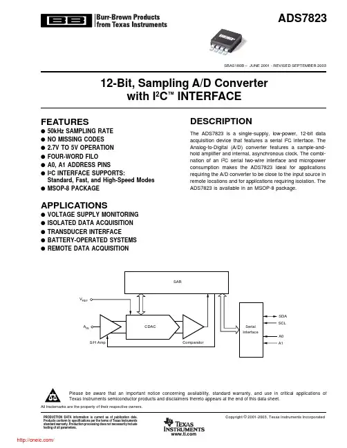
12-Bit, Sampling A/D Converterwith I2C™ INTERFACEFEATURESq50kHz SAMPLING RATEq NO MISSING CODESq2.7V TO 5V OPERATIONq FOUR-WORD FILOq A0, A1 ADDRESS PINSq I2C INTERFACE SUPPORTS:Standard, Fast, and High-Speed Modesq MSOP-8 PACKAGEAPPLICATIONSq VOLTAGE SUPPLY MONITORINGq ISOLATED DATA ACQUISITIONq TRANSDUCER INTERFACEq BATTERY-OPERATED SYSTEMSq REMOTE DATA ACQUISITIONDESCRIPTIONThe ADS7823 is a single-supply, low-power, 12-bit dataacquisition device that features a serial I2C interface. TheAnalog-to-Digital (A/D) converter features a sample-and-hold amplifier and internal, asynchronous clock. The combi-nation of an I2C serial two-wire interface and micropowerconsumption makes the ADS7823 ideal for applicationsrequiring the A/D converter to be close to the input source inremote locations and for applications requiring isolation. TheADS7823 is available in an MSOP-8 package.SDASCLA0A1AV REFADS7823SBAS180B – JUNE 2001 - REVISED SEPTEMBER 2003Copyright © 2001-2003, Texas Instruments Incorporated Please be aware that an important notice concerning availability, standard warranty, and use in critical applications ofTexas Instruments semiconductor products and disclaimers thereto appears at the end of this data sheet.PRODUCTION DATA information is current as of publication date.Products conform to specifications per the terms of Texas Instrumentsstandard warranty. Production processing does not necessarily includetesting of all parameters.All trademarks are the property of their respective owners.ADS78232MAXIMUM INTEGRAL SPECIFIED LINEARITY TEMPERATUREPACKAGE PACKAGE ORDERING TRANSPORT PRODUCT ERROR (LSB)RANGE PACKAGE-LEADDESIGNATOR (1)MARKINGNUMBER MEDIA, QUANTITY ADS7823E±2–40°C to +85°CMSOP-8DGKB23ADS7823E/250Tape and Reel, 250""""""ADS7823E/2K5Tape and Reel, 2500ADS7823EB±1–40°C to +85°CMSOP-8DGKB23ADS7823EB/250Tape and Reel, 250""""""ADS7823EB/2K5Tape and Reel, 2500NOTE: (1) For the most current specifications and package information, refer to our web site at .PACKAGE/ORDERING INFORMATIONABSOLUTE MAXIMUM RATINGS (1)+V DD to GND ........................................................................–0.3V to +6V Digital Input Voltage to GND .................................–0.3V to +V DD + 0.3V Analog Input Voltage to GND ...........................................–0.3V to +6.0V Operating Temperature Range ........................................–40°C to +85°C Storage Temperature Range .........................................–65°C to +150°C Junction Temperature (T J max)....................................................+150°C TSSOP PackagePower Dissipation....................................................(T J max – T A )/θJA θJA Thermal Impedance ......................................................+240°C/W Lead Temperature, SolderingVapor Phase (60s)............................................................+215°C Infrared (15s).....................................................................+220°C NOTE: (1) Stresses above those listed under “Absolute Maximum Ratings”may cause permanent damage to the device. Exposure to absolute maximum conditions for extended periods may affect device reliability.This integrated circuit can be damaged by ESD. Texas Instru-ments recommends that all integrated circuits be handled with appropriate precautions. Failure to observe proper handling and installation procedures can cause damage.ESD damage can range from subtle performance degradation to complete device failure. Precision integrated circuits may be more susceptible to damage because very small parametric changes could cause the device not to meet its published specifications.ELECTRICAL CHARACTERISTICS: +2.7VAt T A = –40°C to +85°C, +V DD = +2.7V, V REF = +2.5V, SCL Clock Frequency = 3.4MHz (High Speed Mode) unless otherwise noted.ADS7823EADS7823EBPARAMETER CONDITIONSMINTYPMAX MINTYPMAX UNITS RESOLUTION 12✻Bits ANALOG INPUTFull-Scale Input Range 0V REF✻✻V Input Capacitance 25✻pF Input Leakage Current ±1✻µA SYSTEM PERFORMANCE No Missing Codes 12✻Bits Integral Linearity Error ±1.0 ±2±0.5 ±1LSB (1)Differential Linearity Error –0.5, +1.0 –1.0, +3.0±0.5✻LSB Offset Error ±1.0 ±4±0.75±3LSB Gain Error ±1.0±4±0.75±3LSB Noise33✻µVrms Power Supply Rejection 82✻dB SAMPLING DYNAMICS Throughput FrequencyHigh Speed Mode: SCL = 3.4MHz50✻kHz Fast Mode: SCL = 400kHz 8✻kHz Standard Mode, SCL = 100kHz2✻kHz Conversion Time8✻µs AC ACCURACYTotal Harmonic Distortion V IN = 2.5V PP at 10kHz –82✻dB (2)Signal-to-RatioV IN = 2.5V PP at 10kHz 72✻dB Signal-to-(Noise+Distortion) Ratio V IN = 2.5V PP at 10kHz 71✻dB Spurious Free Dynamic Range V IN = 2.5V PP at 10kHz86✻dBVOLTAGE REFERENCE INPUT Range 0.05V DD✻✻V Resistance All Modes1.0✻G ΩCurrent DrainAt Code 800H, HS Mode: SCL = 3.4MHz9.0✻µAELECTRICAL CHARACTERISTICS: +2.7V (Cont.)At T A = –40°C to +85°C, +V DD = +2.7V, V REF = +2.5V, SCL Clock Frequency = 3.4MHz (High Speed Mode) unless otherwise noted.ADS7823E ADS7823EBPARAMETER CONDITIONS MIN TYP MAX MIN TYP MAX UNITS DIGITAL INPUT/OUTPUTLogic Family CMOS✻Logic Levels: V IH+V DD • 0.7+V DD + 0.5✻✻V V IL–0.3+V DD • 0.3✻✻VV OL At min 3mA Sink Current0.4✻V Input Leakage: I IH V IH = +V DD +0.510✻µAI IL V IL = -0.3-10✻µAData Format Straight✻BinaryADS7823 HARDWARE ADDRESS10010✻Binary POWER SUPPLY REQUIREMENTSPower Supply Voltage, +V DD Specified Performance 2.7 3.6✻✻V Quiescent Current High Speed Mode: SCL = 3.4MHz250370✻✻µAFast Mode: SCL = 400kHz137✻µAStandard Mode, SCL = 100kHz109✻µA Power Dissipation High Speed Mode: SCL = 3.4MHz6801000✻✻µWFast Mode: SCL = 400kHz370✻µWStandard Mode, SCL = 100kHz290✻µW Powerdown Mode High Speed Mode: SCL = 3.4MHz60✻µA w/Wrong Address Selected Fast Mode: SCL = 400kHz23✻µAStandard Mode, SCL = 100kHz 5.4✻µA Full Powerdown SCL Pulled HIGH, SDA Pulled HIGH23000✻✻nA TEMPERATURE RANGESpecified Performance–4085✻✻°C✻ Specifications same as ADS7823E.NOTES: (1) LSB means Least Significant Bit. With V REF equal to 2.5V, 1LSB is 610µV. (2) THD measured out to the 9th-harmonic.ELECTRICAL CHARACTERISTICS: +5VAt T A = –40°C to +85°C, +V DD = +5.0V, V REF = +5.0V, SCL Clock Frequency = 3.4MHz (High Speed Mode) unless otherwise noted.ADS7823E ADS7823EBPARAMETER CONDITIONS MIN TYP MAX MIN TYP MAX UNITS RESOLUTION12✻Bits ANALOG INPUTFull-Scale Input Range0V REF✻✻VInput Capacitance25✻pFInput Leakage Current±1✻µA SYSTEM PERFORMANCENo Missing Codes12✻Bits Integral Linearity Error±1.0±2±0.5±1LSB(1) Differential Linearity Error–0.5, +1.0 –1, +3±0.5✻LSB Offset Error±1.0±4±0.75±3LSB Gain Error±1.0±4±0.75±3LSB Noise33✻µVrms Power Supply Rejection82✻dB SAMPLING DYNAMICSThroughput Frequency High Speed Mode: SCL = 3.4MHz50✻kHzFast Mode: SCL = 400kHz8✻kHzStandard Mode, SCL = 100kHz2✻kHz Conversion Time8✻µsAC ACCURACYTotal Harmonic Distortion V IN = 2.5V PP at 10kHz–82✻dB(2) Signal-to-Ratio V IN = 2.5V PP at 10kHz72✻dB Signal-to-(Noise+Distortion) Ratio V IN = 2.5V PP at 10kHz71✻dB Spurious Free Dynamic Range V IN = 2.5V PP at 10kHz86✻dB VOLTAGE REFERENCE INPUTRange0.05V DD✻✻V Resistance All Modes 1.0✻GΩCurrent Drain At Code 800H, HS Mode: SCL = 3.4MHz20✻µAADS78233 SBAS180BADS78234DIGITAL INPUT/OUTPUT Logic Family CMOS ✻Logic Levels: V IH+V DD • 0.7+V DD + 0.5✻✻V V IL –0.3+V DD • 0.3✻✻V V OLAt min 3mA Sink Current0.4✻V Input Leakage: I IHV IH = +V DD +0.510✻µA I ILV IL = -0.3-10✻µAData FormatStraight ✻Binary ADS7823 HARDWARE ADDRESS 10010✻Binary POWER SUPPLY REQUIREMENTS Power Supply Voltage, +V DD Specified Performance4.755 5.25✻✻V Quiescent CurrentHigh Speed Mode: SCL= 3.4MHz0.72 1.0✻✻mA Fast Mode: SCL= 400kHz 380✻µA Standard Mode, SCL=100kHz 240✻µA Power Dissipation High Speed Mode: SCL= 3.4MHz3.6 5.0✻✻mW Fast Mode: SCL= 400kHz 1.9✻mW Standard Mode, SCL=100kHz 1.2✻mW Powerdown Mode High Speed Mode: SCL= 3.4MHz 346✻µA w/Wrong Address Selected Fast Mode: SCL= 400kHz 136✻µA Standard Mode, SCL=100kHz 34✻µA Full Powerdown SCL Pulled HIGH, SDA Pulled HIGH33000✻✻nA TEMPERATURE RANGE Specified Performance–4085✻✻°C ✻ Specifications same as ADS7823E.NOTES: (1) LSB means Least Significant Bit. With V REF equal to 2.5V, 1LSB is 610µV. (2) THD measured out to the 9th-harmonic.PIN CONFIGURATIONTop ViewMSOPPIN DESCRIPTIONSPIN NAME DESCRIPTION1V REF Reference Input, 2.5V Nominal 2A IN Analog Input.3A0Slave Address Bit 04GND Ground5A1Slave Address Bit 16SDA Serial Data 7SCL Serial Clock8+V DDPower Supply, 3.3V Nominal1234V REF A IN A0GND+V DD SCL SDA A18765ADS7823ELECTRICAL CHARACTERISTICS: +5V (Cont.)At T A = –40°C to +85°C, +V DD = +5.0V, V REF = +5.0V, SCL Clock Frequency = 3.4MHz (High Speed Mode) unless otherwise noted.ADS7823EADS7823EBPARAMETERCONDITIONSMIN TYPMAXMINTYP MAXUNITSTIMING CHARACTERISTICS(1)At T A = –40°C to +85°C, +V DD = +2.7V, unless otherwise noted.PARAMETER SYMBOL CONDITIONS MIN MAX UNITSSCL Clock Frequency f SCL Standard Mode100kHzFast Mode400kHzHigh-Speed Mode, C B = 100pF max 3.4MHzHigh-Speed Mode, C B = 400pF max 1.7MHzBus Free Time Between a STOP and t BUF Standard Mode 4.7µs START Condition Fast Mode 1.3µsHold Time (Repeated) START t HD;STA Standard Mode 4.0µs Condition Fast Mode600nsHigh-Speed Mode160nsLOW Period of the SCL Clock t LOW Standard Mode 4.7µsFast Mode 1.3µsHigh-Speed Mode, C B = 100pF max(2)160nsHigh-Speed Mode, C B = 400pF max(2)320nsHIGH Period of the SCL Clock t HIGH Standard Mode 4.0µsFast Mode600nsHigh-Speed Mode, C B = 100pF max(2)60nsHigh-Speed Mode, C B = 400pF max(2)120nsSetup Time for a Repeated START t SU;STA Standard Mode 4.7µs Condition Fast Mode600nsHigh-Speed Mode160nsData Setup Time t SU;DAT Standard Mode250nsFast Mode100nsHigh-Speed Mode10nsData Hold Time t HD;DAT Standard Mode0 3.45µsFast Mode00.9µsHigh-Speed Mode, C B = 100pF max(2)0(3)70nsHigh-Speed Mode, C B = 400pF max(2)0(3)150nsRise Time of SCL Signal t RCL Standard Mode1000nsFast Mode20 + 0.1C B300nsHigh-Speed Mode, C B = 100pF max(2)1040nsHigh-Speed Mode, C B = 400pF max(2)2080nsRise Time of SCL Signal After a t RCL1Standard Mode1000ns Repeated START Condition and Fast Mode20 + 0.1C B300nsAfter an Acknowledge Bit High-Speed Mode, C B = 100pF max(2)1080nsHigh-Speed Mode, C B = 400pF max(2)20160nsFall Time of SCL Signal t FCL Standard Mode300nsFast Mode20 + 0.1C B300nsHigh-Speed Mode, C B = 100pF max(2)1040nsHigh-Speed Mode, C B = 400pF max(2)2080nsRise Time of SDA Signal t RDA Standard Mode1000nsFast Mode20 + 0.1C B300nsHigh-Speed Mode, C B = 100pF max(2)1080nsHigh-Speed Mode, C B = 400pF max(2)20160nsFall Time of SDA Signal t FDA Standard Mode300nsFast Mode20 + 0.1C B300nsHigh-Speed Mode, C B = 100pF max(2)1080nsHigh-Speed Mode, C B = 400pF max(2)20160nsSetup Time for STOP Condition t SU;STO Standard Mode 4.0µsFast Mode600nsHigh-Speed Mode160ns Capacitive Load for SDA and SCL C B400pFLinePulse Width of Spike Suppressed t SP Fast Mode50nsHigh-Speed Mode10nsNoise Margin at the HIGH Level for Standard ModeEach Connected Device (Including V NH Fast Mode0.2V DD V Hysteresis)High-Speed ModeNoise Margin at the LOW Level for Standard ModeEach Connected Device (Including V NL Fast Mode0.1V DD V Hysteresis)High-Speed ModeNOTES: (1) All values referred to V IHMIN and V ILMAX levels. (2) For bus line loads C B between 100pF and 400pF the timing parameters must be linearly interpolated.(3) A device must internally provide a data hold time to bridge the undefined part between V IH and V IL of the falling edge of the SCLH signal. An input circuit witha threshold as low as possible for the falling edge of the SCLH signal minimizes this hold time.ADS78235 SBAS180BADS78236TYPICAL CHARACTERISTICSAt T A = +25°C, +V DD = +2.7V, V REF = External +2.5V, f SAMPLE= 50kHz, unless otherwise noted.FREQUENCY SPECTRUM (4096 Point FFT, f IN = 1kHz, 0dB)Frequency (kHz)102520A m p l i t u d e (dB )–40–80–120INTEGRAL LINEARITY ERROR vs CODE (+25°C)Hex Code000H800H FFF HI L E (L S B S )1.000.750.500.250–0.25–0.50–0.75–1.00DIFFERENTIAL LINEARITY ERROR vs CODE (+25°C)Hex Code000H800H FFF HD LE (L S B S )1.000.750.500.250–0.25–0.50–0.75–1.00CHANGE IN OFFSET vs TEMPERATURETemperature (°C)–50–250255075100D e l t a f r o m +25°C (L S B )1.51.00.50–0.5–1.0–1.5CHANGE IN GAIN vs TEMPERATURETemperature (°C)–50–25255075100D e l t a f r o m +25°C (L S B )1.51.00.50–0.5–1.0–1.5SUPPLY CURRENT vs TEMPERATURETemperature (°C)–50–25255075100S u p p l y C u r r e n t (µA )400350300250200150100ADS78237SBAS180BTYPICAL CHARACTERISTICS (Cont.)At T A = +25°C, +V DD = +2.7V, V REF = External +2.5V, f SAMPLE = 50kHz, unless otherwise noted.SUPPLY CURRENT vs I 2C BUS RATEI 2C Bus Rate (kHz)10100100010000S u p p l y C u r r e n t (µA )35030025020015010050POWER DOWN SUPPLY CURRENTvs TEMPERATURETemperature (°C)–50–25255075125100S u p p l y C u r r e n t (n A )403020100–10–20ADS78238FIGURE 1. Simplified I/O of the ADS7823.THEORY OF OPERATIONThe ADS7823 is a classic Successive Approximation Register (SAR) A/D converter. The architecture is based on capacitive redistribution which inherently includes a sample-and-hold function. The converter is fabricated on a 0.6µ CMOS process.The ADS7823 core is controlled by an internally-generated free-running clock. When the ADS7823 is not performing conversions or being addressed, it keeps the A/D converter core powered off, and the internal clock does not operate.The ADS7823 has an internal 4-word first-in last-out buffer (FILO) that stores the results of up to four conversions while they are waiting to be read out over the I 2C bus.The simplified diagram of input and output for the ADS7823is shown in Figure 1.ANALOG INPUTWhen the converter enters the hold mode, the voltage on the A IN pin is captured on the internal capacitor array. The input current on the analog inputs depends on the conversion rate of the device. During the sample period, the source must charge the internal sampling capacitor (typically 25pF). After the capacitor has been fully charged, there is no further input current. The amount of charge transfer from the analog source to the converter is a function of conversion rate.REFERENCE INPUTThe external reference sets the analog input range. The ADS7823 will operate with a reference in the range of 50mV to V DD . There are several important implications of this.As the reference voltage is reduced, the analog voltage weight of each digital output code is reduced. This is often referred to as the LSB (least significant bit) size and is equal to the reference voltage divided by 4096. This means that any offset or gain error inherent in the A/D converter will appear to increase, in terms of LSB size, as the reference voltage is reduced.The noise inherent in the converter will also appear to increase with lower LSB size. With a 2.5V reference, the internal noise of the converter typically contributes only 0.32LSB peak-to-peak of potential error to the output code. When the external reference is 50mV, the potential error contribution from the internal noise will be 50 times larger —16LSBs. The errors due to the internal noise are Gaussian in nature and can be reduced by averaging consecutive conversion results.DIGITAL INTERFACEThe ADS7823 supports the I 2C serial bus and data transmis-sion protocol, in all three defined modes: standard, fast, and high-speed. A device that sends data onto the bus is defined as a transmitter, and a device receiving data as a receiver.ADS78239SBAS180BFIGURE 2. Basic Operation of the ADS7823.The device that controls the message is called a “master.”The devices that are controlled by the master are “slaves.”The bus must be controlled by a master device that gener-ates the serial clock (SCL), controls the bus access, and generates the START and STOP conditions. The ADS7823operates as a slave on the I 2C bus. Connections to the bus are made via the open-drain I/O lines SDA and SCL.The following bus protocol has been defined (as shown in Figure 2):•Data transfer may be initiated only when the bus is not busy.•During data transfer, the data line must remain stable whenever the clock line is HIGH. Changes in the data line while the clock line is HIGH will be interpreted as control signals.Accordingly, the following bus conditions have been defined:Bus Not Busy: Both data and clock lines remain HIGH.Start Data Transfer: A change in the state of the data line,from HIGH to LOW, while the clock is HIGH, defines a START condition.Stop Data Transfer: A change in the state of the data line,from LOW to HIGH, while the clock line is HIGH, defines the STOP condition.Data Valid: The state of the data line represents valid data,when, after a START condition, the data line is stable for the duration of the HIGH period of the clock signal. There is one clock pulse per bit of data.Each data transfer is initiated with a START condition and terminated with a STOP condition. The number of data bytes transferred between START and STOP conditions is not limited and is determined by the master device. The informa-tion is transferred byte-wise and each receiver acknowl-edges with a ninth bit.Within the I 2C bus specifications a standard mode (100kHz clock rate), a fast mode (400kHz clock rate), and a high-speed mode (3.4MHz clock rate) are defined. The ADS7823works in all three modes.Acknowledge: Each receiving device, when addressed, is obliged to generate an acknowledge after the reception of each byte. The master device must generate an extra clock pulse that is associated with this acknowledge bit.A device that acknowledges must pull down the SDA line during the acknowledge clock pulse in such a way that the SDA line is stable LOW during the HIGH period of the acknowledge clock pulse. Of course, setup and hold times must be taken into account. A master must signal an end of data to the slave by not generating an acknowledge bit on the last byte that has been clocked out of the slave. In this case,the slave must leave the data line HIGH to enable the master to generate the STOP condition.Figure 2 details how data transfer is accomplished on the I 2C bus. Depending upon the state of the R/W bit, two types of data transfer are possible:1.Data transfer from a master transmitter to a slave receiver. The first byte transmitted by the master is the slave address. Next follows a number of data bytes. The slave returns an acknowledge bit after the slave address and each received byte.2.Data transfer from a slave transmitter to a master receiver. The first byte, the slave address, is transmitted by the master. The slave then returns an acknowledge bit.Next, a number of data bytes are transmitted by the slave to the master. The master returns an acknowledge bit after all received bytes other than the last byte. At the end of the last received byte, a not-acknowledge is returned.The master device generates all of the serial clock pulses and the START and STOP conditions. A transfer is ended with a STOP condition or a repeated START condition. Since a repeated START condition is also the beginning of the next serial transfer, the bus will not be released.The ADS7823 may operate in the following two modes:•Slave Receiver Mode: Serial data and clock are received through SDA and SCL. After each byte is received, an acknowledge bit is transmitted. START and STOP condi-tions are recognized as the beginning and end of a serial transfer. Address recognition is performed by hardware after reception of the slave address and direction bit.•Slave Transmitter Mode: The first byte (the slave ad-dress) is received and handled as in the slave receiver mode. However, in this mode the direction bit will indicate that the transfer direction is reversed. Serial data is trans-mitted on SDA by the ADS7823 while the serial clock is input on SCL. START and STOP conditions are recog-nized as the beginning and end of a serial transfer.ADS782310MSB 654321LSB 0XXXXXMSB 654321LSB 11A1A0R/WADDRESS BYTEThe address byte is the first byte received following the START condition from the master device. The first five bits (MSBs) of the slave address are factory pre-set to 10010.The next two bits of the address byte are the device select bits, A1 and A0. Input pins (A1-A0) on the ADS7823 deter-mine these two bits of the device address for a particular ADS7823. A maximum of four devices with the same pre-set code can therefore be connected on the same bus at one time.The A1-A0 Address Inputs can be connected to V DD or digital ground. The device address is set by the state of these pins upon power-up of the ADS7823.The last bit of the address byte (R/W ) defines the operation to be performed. When set to a “1” a read operation is selected; when set to a “0” a write operation is selected.Following the START condition the ADS7823 monitors the SDA bus, checking the device type identifier being transmit-ted. Upon receiving the 10010 code, the appropriate device select bits, and the R/W bit, the slave device outputs an acknowledge signal on the SDA line.The ADS7823 operating mode is determined by a command byte.The ADS7823 command byte simply consists of three zeros in the most significant bits, while the remaining 5 bits are don ’t cares.INITIATING CONVERSIONProvided the master has write-addressed it, the ADS7823turns on the A/D converter section and begins conversions when it receives bit 5 of the command byte shown in the Command Byte. If the command byte is correct, the ADS7823will return an ACK condition.The converter will ignore any wrong command byte (that is,setting any of the top three MSBs to 1), remain in the A/D converter power-down mode, and reset the internal 4-word stack.The ADS7823 will ignore a second valid command byte if two valid commands are issued consecutively. The ADS7823 will respond with a not-acknowledge, and will go to the A/D con-verter power-down mode after the responded not-acknowledge.COMMAND BYTEFIGURE 3. Typical Read Sequence in F/S Mode.分销商库存信息:TIADS7823E/250ADS7823EB/250ADS7823E/2K5 ADS7823E/2K5G4ADS7823EB/2K5ADS7823EB/2K5G4 ADS7823E/250G4ADS7823EB/250G4ADS7823-28EVM。
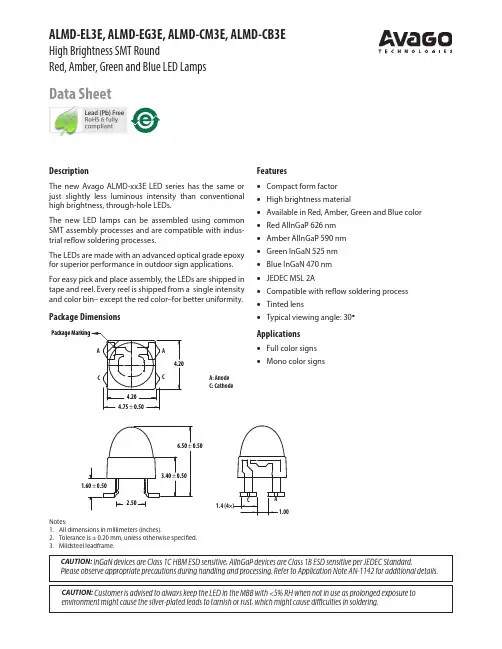
ALMD-EL3E, ALMD-EG3E, ALMD-CM3E, ALMD-CB3EHigh Brightness SMT RoundRed, Amber, Green and Blue LED LampsData SheetFeatures• Compact form factor • High brightness material• Available in Red, Amber, Green and Blue color • Red AlInGaP 626 nm • Amber AlInGaP 590 nm • Green InGaN 525 nm • Blue InGaN 470 nm • JEDEC MSL 2A• Compatible with reflow soldering process • Tinted lens• Typical viewing angle: 30°Applications• Full color signs • Mono color signsNotes:1. All dimensions in millimeters (inches).2. Tolerance is ± 0.20 mm, unless otherwise specified.3. Mildsteel leadframe.DescriptionThe new Avago ALMD-xx3E LED series has the same or just slightly less luminous intensity than conventional high brightness, through-hole LEDs.The new LED lamps can be assembled using common SMT assembly processes and are compatible with indus-trial reflow soldering processes.The LEDs are made with an advanced optical grade epoxy for superior performance in outdoor sign applications. For easy pick and place assembly, the LEDs are shipped in tape and reel. Every reel is shipped from a single intensity and color bin– except the red color–for better uniformity.Package DimensionsCAUTION: InGaN devices are Class 1C HBM ESD sensitive, AlInGaP devices are Class 1B ESD sensitive per JEDEC Standard.Please observe appropriate precautions during handling and processing. Refer to Application Note AN-1142 for additional details.CAUTION: Customer is advised to always keep the LED in the MBB with <5% RH when not in use as prolonged exposure to environment might cause the silver-plated leads to tarnish or rust, which might cause difficulties in soldering.1.4Package MarkingA: Anode C: CathodeDevice Selection GuidePart Number Color and Dominant Wavelengthλd (nm) Typ. [3]Luminous Intensity Iv (mcd) [1,2,5]Viewing AngleTyp. (°) [4] Min.Max.ALMD-EG3E-VX002Red 6264200930030°ALMD-EL3E-VX002Amber 59042009300ALMD-CM3E-Y1002Green 525930021000ALMD-CB3E-SU002Blue 47019004200Notes:1. The luminous intensity is measured on the mechanical axis of the lamp package and it is tested with pulsing condition.2. The optical axis is closely aligned with the package mechanical axis.3. Dominant wavelength, λd, is derived from the CIE Chromaticity Diagram and represents the color of the lamp.4. θ½ is the off-axis angle where the luminous intensity is half the on-axis intensity.5. Tolerance for each bin limit is ± 15%.Part Numbering SystemA L M D-x1x2x3x4-x5x6x7x8x9Code Description Optionx1Package type EC Round AlInGaP Round InGaNx2Color BGLM Blue Red Amber Greenx3Viewing angle330°x4Product specific designation Ex5Minimum intensity bin Refer to device selection guidex6Maximum intensity bin Refer to device selection guidex7Color bin selection0Full distributionx8x9Packaging option 02Tested 20mA, 13inch carrier tapeAbsolute Maximum Rating, T J = 25 °CParameter Red and Amber Green Blue Unit DC Forward Current [1]503020mA Peak Forward Current100 [2]100 [3]100 [3]mA Power Dissipation12011476mW LED Junction Temperature110°C Operating Temperature Range-40 to +85°C Storage Temperature Range-40 to +100°C Notes:1. Derate linearly as shown in Figure 4 and Figure 9.2. Duty Factor 30%, frequency 1 kHz.3. Duty Factor 10%, frequency 1 kHz.Electrical / Optical Characteristics, T J = 25 °CParameter Symbol Min.Typ.Max.Units Test ConditionsForward Voltage RedAmberGreenBlue V F1.81.82.82.82.12.13.23.22.42.43.83.8V I F = 20 mAReverse Voltage [3] Red & Amber Green & Blue V R55V I R = 100 µAI R = 10 µADominant Wavelength [1] RedAmberGreenBlue λd618.0584.5519.0460.0626.0590.0525.0470.0630.0594.5539.0480.0I F = 20 mAPeak Wavelength RedAmberGreenBlue λPEAK634594516464nm Peak of Wavelength of SpectralDistribution at I F = 20 mAThermal Resistance RedAmberGreenBlue RθJ-PIN270270270480°C/W LED Junction-to-PinLuminous Efficacy [2] RedAmberGreenBlue ηV20049053065lm/W Emitted Luminous Power/EmittedRadiant PowerThermal coefficient of λd RedAmberGreenBlue 0.0590.1030.0280.024nm/°C I F = 20 mA ; +25 °C ≤ T J ≤ +100 °CNotes:1. The dominant wavelength is derived from the chromaticity diagram and represents the color of the lamp.2. The radiant intensity, I e in watts per steradian, may be found from the equation I e = I V/ηV where I V is the luminous intensity in candelas and ηV isthe luminous efficacy in lumens/watt.3. Indicates product final testing condition. Long-term reverse bias is not recommended.Figure 1. Relative Intensity vs. Wavelength Figure 2. Forward Current vs. Forward VoltageFigure 3. Relative Intensity vs. Forward Current Figure 4. Maximum Forward Current vs. Ambient TemperatureFigure 5. Relative Dominant Wavelength Shift vs. Forward Current0.00.20.40.60.81.0500550600650AmberRed010203040506000.51 1.52 2.530.00.51.01.52.02.53.001020304050600102030405060-0.8-0.6-0.4-0.200.20.40.60.811.20102030405060WAVELENGTH - nmR E L A T I V E I N T E N S I T YFORWARD VOLTAGE - VF O R W A R D C U R R E N T - m AT A - AMBIENT TEMPERATURE - °CM A X I M U M F O R W A R D C U R R E N T - m ARedAmberFORWARD CURRENT - mAR E L A T I V E L U M I N O U S I N T E N S I T Y (N O R M A L I Z E D A T 20 m A )RedAmberFORWARD CURRENT - mAR E L A T I V E D O M I N A N T W A V E L E N G T H S H I F T - n mFigure 6. Relative Intensity vs. WavelengthFigure 7. Forward Current vs. Forward VoltageFigure 8. Relative Intensity vs. Forward Current Figure 9. Maximum Forward Current vs. Ambient TemperatureFigure 10. Dominant Wavelength Shift vs. Forward Current010*********406080100-10-50510020406080100GreenBlueFORWARD CURRENT - mAR E L A T I V E D O M I N A N T W A V E L E N G T H S H I F T (N O R M A L I Z E D A T 20 m A )T A - AMBIENT TEMPERATURE - °CM A X I M U M F O R W A R D C U R R E N T - m ABlueGreen0.00.10.20.30.40.50.60.70.80.91.0WAVELENGTH - nmR E L A T I V E I N T E N S I T YGREEN BLUE 05101520253001234FORWARD VOLTAGE - VF O R W A R D C U R R E N T - m A 0.00.20.40.60.81.01.21.451015202530DC FORWARD CURRENT - mAR E L A T I V E L U M I N O U S I N T E N S I T Y (N O R M A L I Z E D A T 20 m A )Figure 11a. Radiation Pattern for x-axis Figure 11b. Component Axis for Radiation PatternFigure 12. Relative Intensity Shift vs. Junction Temperature Figure 13. Forward Voltage Shift vs. Junction TemperatureFigure 14. Recommended Soldering Land PatternNote: Recommended stencil thickness is 0.1524mm (6 mils) minimum andabove00.20.40.60.81-90-60-300306090ANGULAR DISPLACEMENT-DEGREEN O R M A L I Z E D I N T E N S I T YN O R M A L Z I E D I N T E N S I T Y (P H O T O )TJ - JUNCTION TEMPERATURE (°C)F O R W A R D V O L T AG E SHI F T - VTJ - JUNCTION TEMPERATURE (°C)Figure 17. Unit Orientation from reel Figure 15. Carrier Tape DimensionIntensity Bin Limit Table (1.3:1 Iv bin ratio)Bin Intensity (mcd) at 20 mA Min.Max.S1******* T25003200 U32004200 V42005500 W55007200 X72009300 Y930012000 Z1200016000 11600021000 Tolerance for each bin limit is ± 15%V F Bin Table (V at 20 mA) for Red and Amber only Bin ID Min.Max. V D 1.8 2.0 V A 2.0 2.2 V B 2.2 2.4 Tolerance for each bin limit is ± 0.05 VRed Color RangeMin Dom Max Dom X min Y Min X max Y max 618.0630.00.68720.31260.68900.29430.66900.31490.70800.2920 Tolerance for each bin limit is ± 0.5nmAmber Color RangeBin MinDomMaxDom Xmin Ymin Xmax Ymax1584.5587.00.54200.45800.55300.44000.53700.45500.55700.4420 2587.0589.50.55700.44200.56700.42500.55300.44000.57200.4270 4589.5592.00.57200.42700.58200.41100.56700.42500.58700.4130 6592.0594.50.58700.41300.59500.39800.58200.41100.60000.3990 Tolerance for each bin limit is ± 0.5nm Green Color RangeBinMinDomMaxDom Xmin Ymin Xmax Ymax 1519.0523.00.06670.83230.14500.73190.12000.73750.09790.8316 2523.0527.00.09790.83160.17110.72180.14500.73190.13050.8189 3527.0531.00.13050.81890.19670.70770.17110.72180.16250.8012 4531.0535.00.16250.80120.22100.69200.19670.70770.19290.7816 5535.0539.00.19290.78160.24450.67470.22100.69200.22330.7600 Tolerance for each bin limit is ± 0.5nmBlue Color RangeBinMinDomMaxDom Xmin Ymin Xmax Ymax 1460.0464.00.14400.02970.17660.09660.18180.09040.13740.0374 2464.0468.00.13740.03740.16990.10620.17660.09660.12910.0495 3468.0472.00.12910.04950.16160.12090.16990.10620.11870.0671 4472.0476.00.11870.06710.15170.14230.16160.12090.10630.0945 5476.0480.00.10630.09450.13970.17280.15170.14230.09130.1327 Tolerance for each bin limit is ± 0.5nmNote: Acronyms and Definition:BIN:(i) Color bin only or V F bin only(Applicable for part number with color bins but with-out V F bin or part number with V F bins and no color bin) (ii) Color bin incorporated with V F binApplicable for part number that have both color bin and V F bin Example:a. Color bin only or V F bin only BIN: 4 (represent color bin 4 only) BIN: V A (represent V F bin “V A” only)b. Color bin incorporate with V F binBIN: 4 VAVA: VF bin “VA”4: Color bin 4 onlyPacking Label(i) Mother Label (Available on MBB bag) (ii) Baby Label (Available on Plastic Reel)SolderingRecommended reflow soldering condition:a. Reflow soldering must not be done more than twotimes. Do observe necessary precautions for handling a moisture-sensitive device, as stated in the following section.b. Recommended board reflow direction:(i) Leaded reflow soldering:(ii) Lead-free reflow soldering:c. Do not apply any pressure or force on the LED during reflow and after reflow when the LED is still hot.d. It is preferred that you use reflow soldering to solder the LED. Use hand soldering only for rework if unavoidable but must be strictly controlled to the following conditions:- Soldering iron tip temperature = 320 °C max.- Soldering duration = 3 sec max.- Number of cycles = 1 only- Power of soldering iron = 50 W max.e. Do not touch the LED body with a hot soldering iron except the soldering terminals as this may damage the LED.f. For de-soldering, it is recommended to use appropriate double head soldering iron. User is advised to confirm beforehand whether the functionality and performance of the LED is affected by hand soldering.TIMETIMET E M P E R A T U RE11PRECAUTIONARY NOTES1. Handling precautionsFor automated pick and place, Avago has tested nozzle size below made with urethane material to be working fine with this LED. However, due to the possibility of variations in other parameters such as pick and place machine maker/model and other settings of the ma-chine, customer is recommended to verify the nozzle selected.d. Control of assembled boards- If the PCB soldered with the LEDs is to be subjected to other high temperature processes, the PCB need to be stored in sealed MBB with desiccant or desiccator at <5%RH to ensure that all LEDs have not exceeded their floor life of 672 hours.e. Baking is required if:- The HIC indicator is not BROWN at 10% and is AZURE at 5%.- The LEDs are exposed to condition of >30°C / 60% RH at any time.- The LED floor life exceeded 672hrs.The recommended baking condition is: 60±5ºC for 20hrs. Baking should only be done once. f. Storage- The soldering terminals of these Avago LEDs are silver plated. If the LEDs are being exposed in ambient environment for too long, the silver plating might be oxidized and thus affecting its solderability performance. As such, unused LEDs must be kept in sealed MBB with desiccant or in desiccator at <5%RH.3. Application precautionsa. Drive current of the LED must not exceed the maximum allowable limit across temperature as stated in the datasheet. Constant current driving is recommended to ensure consistent performance.b. LED is not intended for reverse bias. Do use other appropriate components for such purpose. When driving the LED in matrix form, it is crucial to ensure that the reverse bias voltage is not exceeding the allowable limit of the LED.c. Avoid rapid change in ambient temperature especially in high humidity environment as this will cause condensation on the LED.d. If the LED is intended to be used in outdoor or harsh environment, the LED leads must be protected with suitable potting material against damages caused by rain water, oil, corrosive gases etc. It is recommended to have louver or shade to reduce direct sunlight on the LEDs.4. Eye safety precautionsLEDs may pose optical hazards when in operation. It is not advisable to view directly at operating LEDs as it may be harmful to the eyes. For safety reasons, use ap-propriate shielding or personal protective equipments.Note:1. Nozzle tip should touch the LED flange during pick and place.2. Outer dimensions of the nozzle should be able to fit into the carrier tape pocket.2. Handling of moisture-sensitive deviceThis product has a Moisture Sensitive Level 2a rating per JEDEC J-STD-020. Refer to Avago Application Note AN5305, Handling of Moisture Sensitive Surface Mount Devices, for additional details and a review of proper handling procedures.a. Before use- An unopened moisture barrier bag (MBB) can be stored at <40°C/90%RH for 12 months. If the actual shelf life has exceeded 12 months and the humidity Indicator Card (HIC) indicates that baking is not required, then it is safe to reflow the LEDs per the original MSL rating.- It is recommended that the MBB not be opened prior to assembly (e.g. for IQC). b. Control after opening the MBB- The humidity indicator card (HIC) shall be read immediately upon opening of MBB.- The LEDs must be kept at <30°C / 60%RH at all times and all high temperature related processes including soldering, curing or rework need to be completed within 672 hours.c. Control for unfinished reel- Unused LEDs must be stored in a sealed MBB with desiccant or desiccator at <5%RH.>3.5mmFor product information and a complete list of distributors, please go to our web site: Avago, Avago Technologies, and the A logo are trademarks of Avago Technologies in the United States and other countries.Data subject to change. Copyright © 2005-2015 Avago Technologies. All rights reserved. AV02-4540EN - April 27, 2015DISCLAIMER: Avago’s products and sof tware are not specifically designed, manuf actured or authorized f or sale as parts, components or assemblies for the planning, construction, maintenenace or direct operation of a nuclear facility or for use in medical devices or applications. Customer is solely responsible, and waives all rights to make claims against avago or its suppliers, for all loss, damage, expense or liability in connection with such use.。
No.1,XianKe Yi Road , Huadong town ,Huadu district,Guangzhou,ChinaDATE: 日期:工程技术中心鸿利智汇集广州分公司ATTENTION注意OBSERVE PRECAUTIONS FOR HANDLINGELECTROSTATICDISCHARGESENSITIVEDEVICES请勿裸手接触器件Label on ESD shielding 静电袋上标签Label on box 外箱标签V: Luminous Flux rank 光通量档次范围VF: Forward voltage rank 正向电压档次范围TC: Color temperature 色温SDCM: 相对色容差Packing figure 包装图Precaution for use (防护措施)1. Storage储存To avoid moisture, we recommend storage conditions for the unopened LED +5 ~ +30 °C, rela-tive humidity <60%. LED should be used within 168 Hrs. of opening the package. Please make sure to dehumidify and vacuum pack the remaining/ unused LED. Dehumidifying condition: +120 ° C ± 5 ° C, 04 Hrs. Effective age for the sealed led is one year.为避免受潮的影响,我司建议产品在未开包装前储存条件为 5-30°C,相对湿度小于 60%。
已开包装的 LED 光源请在 168H 内使用安装完毕,如未用完之产品,请进行除湿并抽真空后密封保存。
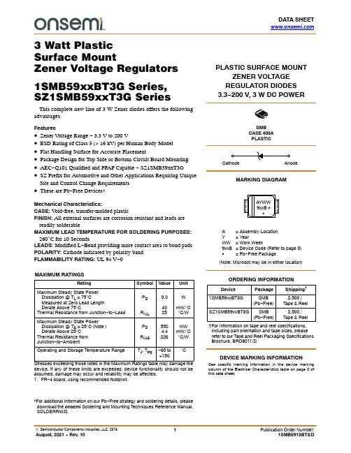
DATA SHEET 3 Watt PlasticSurface MountZener Voltage Regulators1SMB59xxBT3G Series,SZ1SMB59xxT3G SeriesThis complete new line of 3 W Zener diodes offers the followingadvantages.Features•Zener V oltage Range − 3.3 V to 200 V•ESD Rating of Class 3 (> 16 kV) per Human Body Model•Flat Handling Surface for Accurate Placement•Package Design for Top Side or Bottom Circuit Board Mounting•AEC−Q101 Qualified and PPAP Capable − SZ1SMB59xxT3G•SZ Prefix for Automotive and Other Applications Requiring UniqueSite and Control Change Requirements•These are Pb−Free Devices*Mechanical Characteristics:CASE:V oid-free, transfer-molded plasticFINISH:All external surfaces are corrosion resistant and leads arereadily solderableMAXIMUM LEAD TEMPERATURE FOR SOLDERING PURPOSES:260°C for 10 SecondsLEADS:Modified L−Bend providing more contact area to bond padsPOLARITY:Cathode indicated by polarity bandFLAMMABILITY RATING:UL 94 V−0MAXIMUM RATINGSRating Symbol Value UnitMaximum Steady State Power Dissipation @ T L = 75°CMeasured at Zero Lead LengthDerate Above 75°CThermal Resistance from Junction−to−LeadP DR qJL3.04025WmW/°C°C/WMaximum Steady State Power Dissipation @ T A = 25°C (Note ) Derate Above 25°CThermal Resistance from Junction−to−AmbientP DR q JA5504.4226mWmW/°C°C/WOperating and Storage Temperature Range T J, T stg−65 to+150°CStresses exceeding those listed in the Maximum Ratings table may damage the device. If any of these limits are exceeded, device functionality should not be assumed, damage may occur and reliability may be affected.1.FR−4 board, using recommended footprint.*For additional information on our Pb−Free strategy and soldering details, please download the onsemi Soldering and Mounting T echniques Reference Manual, SOLDERRM/D.PLASTIC SURFACE MOUNTZENER VOLTAGEREGULATOR DIODES3.3−200 V, 3 W DC POWERSMBCASE 403APLASTICMARKING DIAGRAMDevice Package Shipping†ORDERING INFORMATION1SMB59xxBT3G SMB(Pb−Free)2,500 /Tape & Reel†For information on tape and reel specifications, including part orientation and tape sizes, please refer to our T ape and Reel Packaging Specifications Brochure, BRD8011/D.A= Assembly LocationY= YearWW= Work Week9xxB= Device Code (Refer to page 3)G= Pb−Free PackageAYWW9xxB GG(Note: Microdot may be in either location)See specific marking information in the device marking column of the Electrical Characteristics table on page 3 of this data sheet.DEVICE MARKING INFORMATIONSZ1SMB59xxBT3G SMB(Pb−Free)2,500 /Tape & ReelELECTRICAL CHARACTERISTICS (T L = 30°C unless otherwise noted,V F = 1.5 V Max. @ I F = 200 mA(dc) for all types) Symbol Parameter V Z Reverse Zener Voltage @ I ZTI ZT Reverse CurrentZZT Maximum Zener Impedance @ I ZT I ZK Reverse CurrentZ ZK Maximum Zener Impedance @ I ZKI R Reverse Leakage Current @ V RV R Reverse VoltageI F Forward CurrentV F Forward Voltage @ I FI ZM Maximum DC Zener CurrentELECTRICAL CHARACTERISTICS (T L = 30°C unless otherwise noted, V F = 1.5 V Max. @ I F = 200 mA(dc) for all types) (Devices listed in bold, italic are onsemi Preferred devices.)Device* (Note 2)DeviceMarkingZener Voltage (Note 3)Zener Impedance (Note 4)Leakage CurrentI ZMV Z(Volts)@ I ZT Z ZT@ I ZT Z ZK@ I ZK I R@ V RMin Nom Max mA W W mA m A Volts mA(dc)1SMB5913BT3G913B 3.13 3.3 3.47113.61050011001454 1SMB5914BT3G914B 3.42 3.6 3.78104.295001751416 1SMB5915BT3G915B 3.70 3.9 4.1096.17.55001251384 1SMB5916BT3G916B 4.08 4.3 4.5287.26500151348 1SMB5917BT3G917B 4.46 4.7 4.9479.8550015 1.5319 1SMB5918BT3G918B 4.84 5.1 5.3673.54350152294 1SMB5919BT3G919B 5.32 5.6 5.8866.92250153267 1SMB5920BT3G920B 5.89 6.2 6.5160.52200154241 1SMB5921BT3G921B 6.46 6.87.1455.1 2.520015 5.2220 1SMB5922BT3G922B7.127.57.885034000.556200 1SMB5923BT3G923B7.798.28.6145.7 3.54000.55 6.5182 1SMB5924BT3G924B8.649.19.5641.245000.557164 1SMB5925BT3G925B9.51010.537.5 4.55000.2558150 1SMB5926BT3G926B10.451111.5534.1 5.55500.2518.4136 1SMB5927BT3G927B11.41212.631.2 6.55500.2519.1125 1SMB5928BT3G928B12.351313.6528.875500.2519.9115 1SMB5929BT3G929B14.251515.752596000.25111.4100 1SMB5930BT3G930B15.21616.823.4106000.25112.293 1SMB5931BT3G931B17.11818.920.8126500.25113.783 1SMB5932BT3G932B19202118.7146500.25115.275 1SMB5933BT3G933B20.92223.11717.56500.25116.768 1SMB5934BT3G934B22.82425.215.6197000.25118.262 1SMB5935BT3G935B25.652728.3513.9237000.25120.655 1SMB5936BT3G936B28.53031.512.5287500.25122.850 1SMB5937BT3G937B31.353334.6511.4338000.25125.145 1SMB5938BT3G938B34.23637.810.4388500.25127.441 1SMB5939BT3G939B37.053940.959.6459000.25129.738 1SMB5940BT3G940B40.854345.158.7539500.25132.734 1SMB5941BT3G941B44.654749.3586710000.25135.831 1SMB5942BT3G942B48.455153.557.37011000.25138.829 1SMB5943BT3G943B53.25658.8 6.78613000.25142.626 1SMB5944BT3G944B58.96265.1610015000.25147.124 1SMB5945BT3G945B64.66871.4 5.512017000.25151.722 1SMB5946BT3G946B71.257578.75514020000.2515620 1SMB5947BT3G947B77.98286.1 4.616025000.25162.218 1SMB5948BT3G948B86.459195.55 4.120030000.25169.216 1SMB5949BT3G949B95100105 3.725031000.2517615 1SMB5951BT3G951B114120126 3.138045000.25191.212 1SMB5952BT3G952B123.5130136.5 2.945050000.25198.811 1SMB5953BT3G953B142.5150157.5 2.560060000.25111410 1SMB5954BT3G954B152160168 2.370065000.251121.69 1SMB5955BT3G955B171180189 2.190070000.251136.88 1SMB5956BT3G956B190200210 1.9120080000.25115272.TOLERANCE AND TYPE NUMBER DESIGNATION The type numbers listed indicate a tolerance of ±5%.3.ZENER VOLTAGE (V Z) MEASUREMENTNominal Zener voltage is measured with the device junction in thermal equilibrium with ambient temperature at 25°C.4.ZENER IMPEDANCE (Z Z) DERIVATION Z ZT and Z ZK are measured by dividing the ac voltage drop across the device by the ac currentapplied. The specified limits are for I Z(ac) = 0.1 I Z(dc) with the ac frequency = 60 Hz.*Include SZ-prefix devices where applicable.Figure 1. Steady State Power Derating255075100125150654320T, TEMPERATURE (°C)P , M A X I M U M P O W E R D I S S I P A T I O N (W A T T S )D 102030501002003005001K PW, PULSE WIDTH (ms)P , P E A K S U R G E P O W E R (W A T T S )P KFigure 2. Maximum Surge PowerFigure 3. Zener Voltage − To 12 Volts1086420-2-4V Z , ZENER VOLTAGE (VOLTS), T E M P E R A T U R E C O E F F I C I E N T (m V / C )°θV Z 0123456789101005030201010.50.30.20.1V Z , ZENER VOLTAGE (VOLTS)2530102030405060708090100V Z , ZENER VOLTAGE (VOLTS)1005030201010.50.30.20.12531T LT AFigure 4. Zener Voltage − 14 To 200 Volts20010070503020101020305070100200V Z , ZENER VOLTAGE (VOLTS), T E M P E R A T U R E C O E F F I C I E N T (m V / C )°θV Z Figure 5. V Z = 3.3 thru 10 Volts Figure 6. V Z = 12 thru 82 VoltsI Z T , R E V E R S E C U R R E N T (m A )I Z T , R E V E R S E C U R R E N T (m A )Figure 7. Effect of Zener VoltageV Z , ZENER VOLTAGE (VOLTS)57102030507010020010070503020107532Z , D Y N A M I C I M P E D A N C E (O H M S )ZFigure 8. Effect of Zener CurrentI Z , ZENER TEST CURRENT (mA)1k 500200100502010521Z , D Y N A M I C I M P E D A N C E (O H M S )Z Rating and Typical Characteristic Curves (TA = 25°C)Figure 9. Capacitance Curve Figure 10. Typical Pulse Rating CurveBREAKDOWN VOLTAGE (VOLTS)Figure 11. Pulse WaveformT P , PULSE WIDTH (ms)t, TIME (ms)C , C A P A C I T A N C E (p F )P p k 0.9 I 0.1 I I p p m , P E A K P U L S E, P E A K P O W E R (k W )SMBCASE 403A−03ISSUE JDATE 19 JUL 2012SCALE 1:1cNOTES:1.DIMENSIONING AND TOLERANCING PER ANSI Y14.5M, 1982.2.CONTROLLING DIMENSION: INCH.3.DIMENSION b SHALL BE MEASURED WITHIN DIMENSION L1.XXXXX= Specific Device CodeA= Assembly LocationY= YearWW= Work WeekG= Pb−Free Package(Note: Microdot may be in either location)*This information is generic. Please refer todevice data sheet for actual part marking.Pb−Free indicator, “G” or microdot “ G”,may or may not be present.AYWWXXXXX GGGENERICMARKING DIAGRAM*ǒmminchesǓSCALE 8:1*For additional information on our Pb−Free strategy and solderingdetails, please download the ON Semiconductor Soldering andMounting Techniques Reference Manual, SOLDERRM/D.SOLDERING FOOTPRINT*DIMAMIN NOM MAX MINMILLIMETERS1.952.30 2.470.077INCHESA10.050.100.200.002b 1.96 2.03 2.200.077c0.150.230.310.006D 3.30 3.56 3.950.130E 4.06 4.32 4.600.160L0.76 1.02 1.600.0300.0910.0970.0040.0080.0800.0870.0090.0120.1400.1560.1700.1810.0400.063NOM MAX5.21 5.44 5.600.2050.2140.220H E0.51 REF0.020 REFL1SCALE 1:1AYWWXXXXX GGPolarity Band Non−Polarity Band Polarity Band Non−Polarity BandMECHANICAL CASE OUTLINEPACKAGE DIMENSIONSON Semiconductor and are trademarks of Semiconductor Components Industries, LLC dba ON Semiconductor or its subsidiaries in the United States and/or other countries.ON Semiconductor reserves the right to make changes without further notice to any products herein. ON Semiconductor makes no warranty, representation or guarantee regarding the suitability of its products for any particular purpose, nor does ON Semiconductor assume any liability arising out of the application or use of any product or circuit, and specifically disclaims any and all liability, including without limitation special, consequential or incidental damages. ON Semiconductor does not convey any license under its patent rights nor thePUBLICATION ORDERING INFORMATIONTECHNICAL SUPPORTNorth American Technical Support:Voice Mail: 1 800−282−9855 Toll Free USA/Canada Phone: 011 421 33 790 2910LITERATURE FULFILLMENT :Email Requests to:*******************onsemi Website: Europe, Middle East and Africa Technical Support:Phone: 00421 33 790 2910For additional information, please contact your local Sales Representative。
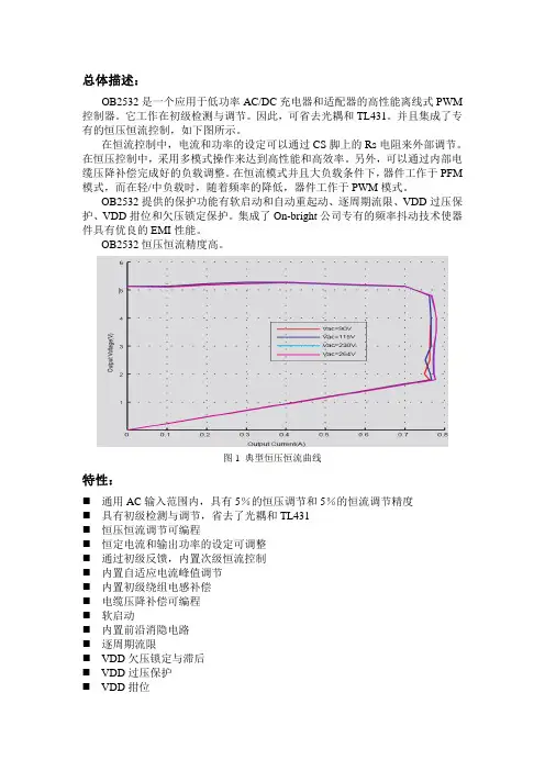
总体描述:OB2532是一个应用于低功率AC/DC充电器和适配器的高性能离线式PWM 控制器。
它工作在初级检测与调节。
因此,可省去光耦和TL431。
并且集成了专有的恒压恒流控制,如下图所示。
在恒流控制中,电流和功率的设定可以通过CS脚上的Rs电阻来外部调节。
在恒压控制中,采用多模式操作来达到高性能和高效率。
另外,可以通过内部电缆压降补偿完成好的负载调整。
在恒流模式并且大负载条件下,器件工作于PFM 模式,而在轻/中负载时,随着频率的降低,器件工作于PWM模式。
OB2532提供的保护功能有软启动和自动重起动、逐周期流限、VDD过压保护、VDD拑位和欠压锁定保护。
集成了On-bright公司专有的频率抖动技术使器件具有优良的EMI性能。
OB2532恒压恒流精度高。
图1 典型恒压恒流曲线特性:⏹通用AC输入范围内,具有5%的恒压调节和5%的恒流调节精度⏹具有初级检测与调节,省去了光耦和TL431⏹恒压恒流调节可编程⏹恒定电流和输出功率的设定可调整⏹通过初级反馈,内置次级恒流控制⏹内置自适应电流峰值调节⏹内置初级绕组电感补偿⏹电缆压降补偿可编程⏹软启动⏹内置前沿消隐电路⏹逐周期流限⏹VDD欠压锁定与滞后⏹VDD过压保护⏹VDD拑位应用低功率AC/DC 离线式开关电源用于 ⏹ 手机充电器⏹ 数字摄像机充电器 ⏹ 小功率适配器⏹ 个人电脑、电视等的辅助电源 ⏹ 线性调节器/RCC 替代 OB2532提供SOT23-6封装典型应用T一般信息引脚结构SOT23-6封装引脚图如下所示注意:漏级引脚连接到100mm PCB铜泊些或其它超过“推荐工作条件”的状态都不是默认的。
长时间工作在绝对最大额定状态会影响器件可靠性。
标记信息Y:年编号(0-9) WW:周编号(01-52) S:网络编号(可选的)引脚分配内部原理图电气特性注意:1、F req_Max表示IC内部的最大时钟频率。
在系统应用中,60KHz额定的最大工作频率存在于最大输出功率或是恒压到恒流的转变点。
OB2532的LED恒流源驱动设计编写:梁炯名3.1芯片介绍LED驱动芯片是LED的另外一个重点,不同芯片有着不同的外围电路,而且所驱动的LED亮度也参差不齐,价格差异就更大了。
出于这两个原因,众多芯片中选择了PI的TNY278P和昂宝的OB2532。
首先介绍下PI的TNY278P,低空载功耗,700V内置MOS管,频率抖动降低EMI滤波成本,节能环保保护功能齐全等等,不得不承认PI的芯片是属于高中端的,但是其价格却是令使用者不敢恭维,加上内置MOS管使得芯片散热处理相对较麻烦,调试过程稍有不慎就会令芯片死掉。
加之采样需要光耦,TL431等元件配合完成,成本较高。
昂宝的OB2532目前只有贴片分装,外置MOS管,几乎不用考虑芯片的散热问题;源边反馈,欠压保护,在设计中将省掉类似光耦TL431等元件,无疑会大幅度的降低LED驱动的成本;它内置的软启动更是延长了芯片的寿命,其价格也是能够让大众接受的。
3.1.1芯片引脚简介OB2532 SOT-23-6引脚图如下所示图3-1 OB2532引脚图表3.1芯片引脚说明引脚名引脚号I/O 描述GND 1 O 芯片接地引脚GATE 2 I 外置MOS管的推拉输出栅极驱动CS 3 I 感应输入电流,连接到MOS管电流传感电阻点INV 4 I 连接从辅助绕组输出的分压电阻器COMP 5 I 回路电压补偿VDD 6 I 芯片供电引脚3.1.2芯片工作原理描述OB2532是一种经济高效的PWM控制器,优化离线低功率AC/DC 包括电池充电器和应用适配器。
它可以实现源端检测和调控,从而不需要光耦和TL431,内置的CV和CC 控制精度高,几乎可以满足所有适配器和充电器的需求。
(一)启动电流和启动控制OB2532的启动电流呗设置的很低,这样VDD能够超过欠压保护的阀值,便于芯片的快速启动,使用一个大的启动电阻可以减少功率损耗(二)操作电流OB2532的操作电流低至2.5mA,在低操作电流和多模控制功能下实现高效率(三)软启动OB2532内部软启动功能,以尽量减轻元件在电源启动时的电气过应力。
SOD-123贴片塑封稳压二极管SOD-123 Plastic-Encapsulate Zener Diode特征Featuresz 齐纳击穿阻抗低; Low Zener Impedancez 最大功率耗散500mW; Power Dissipation of 500mW z 高稳定性和可靠性。
High Stability and High Reliability 机械数据Mechanical DataSOD-123z 封装: SOD-123封装SOD-123 Small Outline Plastic Package z 极性: 色环端为负极Polarity: Color band denotes cathode end z 环氧树脂UL 易燃等级Epoxy UL: 94V-0 z安装位置: 任意Mounting Position: Any极限值和温度特性(TA = 25℃ 除非另有规定)Maximum Ratings & Thermal Characteristics (Ratings at 25℃ ambient temperature unless otherwise specified.) 参数 Parameters符号Symbol 数值Value 单位Unit功率消耗Power DissipationPd 500 mW正向压降Forward Voltage @IF=10mA Vf 0.9 V存储温度Storage temperature rangeTs -65-+150℃ 1) Device mounted on ceramic PCB: 7.6mm x 9.4mm x 0.87mm with pad areas 25mm²2) Short duration test pulse used to minimize self-heating effect 3)f=1KHz电特性 (TA = 25℃ 除非另有规定)Electrical Characteristics (Ratings at 25℃ ambient temperature unless otherwise specified).Zener Voltage RangeMaximum Zener Impedance MaximumReverse CurrentVz@Izt IztZzt @Izt Zzk @IzkIzk IR VRTypicalTemperaturecoefficent @IZTC=mV/℃TestCurrentIZTC Device MarkingNom(V) Min(V) Max(V) mA Ω mAuA V Min Max mA BZT52B2V4 2WX 2.4 2.35 2.45 5 100 600 1.050 1.0 -3.5 0 5 BZT52B2V7 2W1 2.7 2.65 2.75 5 100 600 1.020 1.0 -3.5 0 5 BZT52B3V0 2W2 3.0 2.94 3.06 5 95 600 1.010 1.0 -3.5 0 5 BZT52B3V3 2W3 3.3 3.23 3.37 5 95 600 1.0 5 1.0 -3.5 0 5 BZT52B3V6 2W4 3.6 3.53 3.67 5 90 600 1.0 5 1.0 -3.5 0 5 BZT52B3V9 2W5 3.9 3.82 3.98 5 90 600 1.0 3 1.0 -3.5 0 5 BZT52B4V3 2W6 4.3 4.21 4.39 5 90 600 1.0 3 1.0 -3.5 05BZT52B4V7 2W7 4.7 4.61 4.79 5 80 500 1.0 3 2.0 -3.5 0.2 5 BZT52B5V1 2W8 5.1 5.00 5.20 5 60 480 1.0 2 2.0 -2.7 1.2 5 BZT52B5V6 2W9 5.6 5.49 5.71 5 40 400 1.0 1 2.0 -2.0 2.5 5 BZT52B6V2 2WA 6.2 6.08 6.32 5 10 150 1.0 3 4.0 0.4 3.7 5 BZT52B6V8 2WB 6.8 6.66 6.94 5 15 80 1.0 2 4.0 1.2 4.5 5 BZT52B7V5 2WC 7.5 7.35 7.65 5 15 80 1.0 15.0 2.5 5.3 5BZT52B8V2 2WD 8.2 8.04 8.36 5 1580 1.00.7 5.0 3.2 6.2 5 BZT52B9V1 2WE 9.1 8.929.28 5 15 100 1.00.5 6.0 3.8 7.0 5 BZT52B10 2WF 10 9.80 10.20 5 20 150 1.00.2 7.0 4.5 8.0 5 BZT52B11 2WG 11 10.78 11.22 5 20 150 1.00.1 8.0 5.4 9.0 5 BZT52B12 2WH 12 11.76 12.24 5 25 150 1.00.1 8.0 6.0 10.0 5 BZT52B13 2WI 13 12.74 13.26 5 30 170 1.00.1 8.0 7.0 11.051) 2)Zener Voltage RangeMaximum Zener Impedance MaximumReverse CurrentVz@Izt Izt Zzt @Izt Zzk @IzkIzkIR VRTypicalTemperaturecoefficent @IZTC=mV/℃TestCurrentIZTC Device MarkingNom(V) Min(V) Max(V) mA Ω mAuA V Min Max mABZT52B15 2WJ 15 14.70 15.30 5 30 200 1.00.1 10.5 9.2 13.0 5 BZT52B16 2WK 16 15.68 16.32 5 40 200 1.00.1 11.2 10.4 14.0 5 BZT52B18 2WL 18 17.64 18.36 5 45 225 1.00.1 12.6 12.4 16.0 5 BZT52B20 2WM 20 19.60 20.40 5 55 225 1.00.1 14.0 14.4 18.0 5 BZT52B22 2WN 22 21.56 22.44 5 55 250 1.00.1 15.4 16.4 20.0 5 BZT52B24 2WO 24 23.52 24.48 5 70 250 1.00.1 16.8 18.4 22.0 5 BZT52B27 2WP 27 26.46 27.54 2 80 300 0.50.1 18.9 21.4 25.3 2 BZT52B30 2WQ 30 29.40 30.60 2 80 300 0.50.1 21.0 24.4 29.4 2 BZT52B33 2WR 33 32.34 33.66 2 80 325 0.50.1 23.1 27.4 33.4 2 BZT52B36 2WS 36 35.28 36.72 2 90 350 0.50.1 25.2 30.4 37.4 2 BZT52B39 2WT 39 38.22 39.78 2 130 350 0.50.1 27.3 33.4 41.2 2 BZT52B43 2WU 43 41.16 43.84 2 100 700 1.00.1 32.0 10.0 12.0 5 BZT52B47 2WV 47 46.06 47.94 2 100 750 1.00.1 35.0 10.0 12.0 5 BZT52B51 2WW 51 49.98 52.02 2 100 750 1.00.1 38.0 10.0 12.05Breakdown characteristicsat Tj=constant (pulsed)Forward characteristicsAdmissible power dissipation versus ambient temperaturePulse thermal resistance versus pulse durationDynamic resistance versus Zener currentCapacitance versus Zener voltageDynamic resistance versus Zener current Dynamic resistance versus Zener current Thermal differential resistance versus Zener voltageDynamic resistance versus Zener voltageTemperature dependence of Zener voltage versus Zener voltageTemperature dependence of Zener voltage versus Zener voltageChange of Zener voltage versus junction temperatureChange of Zener voltage versus junction temperatureChange of Zener voltge from turn-on up to the point of thermalequilibrium versus Zener voltageSOD-123 PACKAGE OUTLINE Plastic surface mounted package焊盘设计参考Precautions: PCB DesignRecommended land dimensions for SOD-123 diode. Electrode patterns for PCBs中心距: 3.24 脚宽: 0.55 焊盘宽: 1.00 脚长: 0.50 焊盘长: 0.80 技术要求:1, 塑封体尺寸: 2.70 X 1.60 2: 未注公差为: ±0.053, 所有单位: mm。
OCP8122A应⽤电路图纸12V供电.jpg ocp8122a引脚功能和电压应⽤电路图,⼀、描述OCP8122A是⼀款双通道⼤功率LED恒流驱动控制器,适合⼤尺⼨LCDTV背光LED驱动。
OCP8122A集成了两个实现最佳效率独产控制的LED驱动器。
驱动器输出相移180度,使得芯⽚在⼤功率应⽤时有较⼩的纹波电流。
OCP8122A⽀持PWM信号对每个通道进⾏独⽴的调光,模拟调光同时控制两个通道。
它提供系统灵活设计适合LCDTV局部调光或3D显⽰模式。
OCP8122A⽀持配置适合主从操作的多通道应⽤。
同步实现⼀个独⽴单线界⾯的最⼩化系统组件。
OCP8122A有完整的保护功能,例如:MOSFET的过流保护(OCP)、输出对地短路保护(SCP)、输⼊⽋压保护(UVLO)、输出过压保护(OVP)、限流保护。
三、管脚定义及实现的功能9、ADIM为IC模拟调光控制脚,改变VADIM从0.5V⾄1.5V时,LED电流会逐渐增⼤。
当该值⼩于0.5V时IC内部会调整IFB脚到0.2V,当⼤于1.5V时IC内部会调整IFB脚到0.6V。
建议应⽤时,ADIM脚设置为2.5V。
10、Timer为故障关断延迟时间设置脚,应⽤时,需外接⼀个电容。
11、CMP1为外接电容、电阻设置1通道软启动及补偿脚。
12、CMP2为外接电容、电阻设置2通道软启动及补偿脚。
13、IFB2为2通道LED电流采样输⼊脚,LED电流为(ILED=VIFB/R32)。
14、GATE2为2通道外接MOSFET驱动控制脚。
15、OVP2为2通道输出过压保护采样输⼊脚。
16、CS2为2通道Power MOSFET 开关电流采样输⼊脚。
17、IFB1为1通道LED电流采样输⼊脚,LED电流为(ILED=VIFB/R32)。
18、GATE1为1通道外接MOSFET驱动控制脚。
19、OVP1为1通道输出过压保护采样输⼊脚。
20、CS1为1通道Power MOSFET 开关电流采样输⼊脚。
GENERAL DESCRIPTIONNew generation, high-voltage, high-speed switching npn transistor in a plastic envelope intended for use in horizontal deflection circuits of high resolution monitors.QUICK REFERENCE DATASYMBOL PARAMETERCONDITIONS TYP.MAX.UNIT V CESM Collector-emitter voltage peak value V BE = 0-1500V V CEO Collector-emitter voltage (open base)-800V I C Collector current (DC)-16A I CM Collector current peak value -40A P tot Total power dissipationT mb ≤ 25 ˚C-125W V CEsat Collector-emitter saturation voltage I C = 7.0 A; I B = 1.17 A - 5.0V I Csat Collector saturation current f = 82 kHz7-A t sStorage timeI Csat = 7.0 A; f = 82 kHz1.41.8µsPINNING - SOT429PIN CONFIGURATION SYMBOLLIMITING VALUESLimiting values in accordance with the Absolute Maximum Rating System (IEC 134)SYMBOL PARAMETERCONDITIONS MIN.MAX.UNIT V CESM Collector-emitter voltage peak value V BE = 0 V-1500V V CEO Collector-emitter voltage (open base)-800V I C Collector current (DC)-16A I CM Collector current peak value -40A I B Base current (DC)-10A I BM Base current peak value -15A -I B(AV)Reverse base currentaverage over any 20 ms period -200mA -I BM Reverse base current peak value 1-10A P tot Total power dissipation T mb ≤ 25 ˚C-125W T stg Storage temperature -55150˚C T jJunction temperature-150˚CTHERMAL RESISTANCESSYMBOL PARAMETERCONDITIONS TYP.MAX.UNIT R th j-mb Junction to mounting base -- 1.0K/W R th j-aJunction to ambientin free air45-K/W1 Turn-off current.STATIC CHARACTERISTICST mb = 25 ˚C unless otherwise specified SYMBOL PARAMETERCONDITIONSMIN.TYP.MAX.UNIT I CES Collector cut-off current 2V BE = 0 V; V CE = V CESMmax -- 1.0mA I CES V BE = 0 V; V CE = V CESMmax ;-- 2.0mA T j = 125 ˚CI EBO Emitter cut-off currentV EB = 7.5 V; I C = 0 A -- 1.0mA BV EBO Base-emitter breakdown voltage I B = 1 mA7.514-V V CEsat Collector-emitter saturation voltage I C = 7.0 A; I B = 1.17 A -- 5.0V V BEsat Base-emitter saturation voltage I C = 7.0 A; I B = 1.17 A 0.800.880.97Vh FE DC current gainI C = 1 A; V CE = 5 V 91727h FEI C = 7 A; V CE = 5 V6912.5DYNAMIC CHARACTERISTICST mb = 25 ˚C unless otherwise specified SYMBOL PARAMETERCONDITIONSTYP.MAX.UNIT Switching times (82 kHz line I Csat = 7.0 A; L C = 100 µH; C fb = 3 nF;deflection dynamic test circuit).V CC = 138 V; I B(end) = 1.0 At s Turn-off storage time 1.4 1.8µs t fTurn-off fall time0.060.1µs2 Measured with half sine-wave voltage (curve tracer).MECHANICAL DATA1. Refer to mounting instructions for SOT429 envelope.2. Epoxy meets UL94 V0 at 1/8".DEFINITIONSData sheet statusObjective specification This data sheet contains target or goal specifications for product development. Preliminary specification This data sheet contains preliminary data; supplementary data may be published later. Product specification This data sheet contains final product specifications.Limiting valuesLimiting values are given in accordance with the Absolute Maximum Rating System (IEC 134). Stress above one or more of the limiting values may cause permanent damage to the device. These are stress ratings only and operation of the device at these or at any other conditions above those given in the Characteristics sections of this specification is not implied. Exposure to limiting values for extended periods may affect device reliability. Application informationWhere application information is given, it is advisory and does not form part of the specification.© Philips Electronics N.V. 1997All rights are reserved. Reproduction in whole or in part is prohibited without the prior written consent of the copyright owner.The information presented in this document does not form part of any quotation or contract, it is believed to be accurate and reliable and may be changed without notice. No liability will be accepted by the publisher for any consequence of its use. Publication thereof does not convey nor imply any license under patent or other industrial or intellectual property rights.LIFE SUPPORT APPLICATIONSThese products are not designed for use in life support appliances, devices or systems where malfunction of these products can be reasonably expected to result in personal injury. Philips customers using or selling these products for use in such applications do so at their own risk and agree to fully indemnify Philips for any damages resulting from such improper use or sale.。
C ustomer:·Technical Data Sheet PN:XGS-PB2012UB-02 For:IF=20mAContents1.Features2.Applications3.Package dimensions4.Absolute maximum rating5.Electrical optical characteristics6.BIN range7.Package label8.Soldering pad dimensions9.Soldering conditions10.Package tape specifications11.T ypical electro-optical characteristics curves12.Reliability test items and conditions13.Cautions14.Note◆F eatures:Compatible with automatic placement equipmentCompatible with reflow solder processLow power consumption and wide viewing angleThis product doesn’t contain restriction Substance, comply ROHS standard.◆A pplications:Automotive and TelecommunicationFlat backlight for LCD ,switch and symbol in telephone and faxGeneral use for indicators◆P ackage Dimensions:Unit:mmTolerenc e±0.1Electrodes: Ag Plating◆A bsolute Maximum Rating (Ta=25℃)* I FP condition: pulse width ≤1ms ,duty cycle ≤1/10◆E lectrical Optical Characteristics(Ta=25℃)Notes: 1.Tolerance of Luminous Intensity ±10%2.Tolerance of Dominant Wavelength ±2nm3.Tolerance of Forward Voltage ±0.05V4.Luminous Intensity is measured by XGSLED’s equipment on bare chips◆ Soldering Pad Dimensions:◆ S oldering Conditions (Maximum allowable soldering conditions)Reflow soldering profile<Pb-free solder>Time• Reflow soldering should not be done more than two times. • Do not stress its resin while soldering.• After soldering,do not warp the circuit board.T e m p e r a t u r e◆ P ackage Tape Specifications: (3000 pcs/Reel)Reel Lead Min.60mm No LEDs5 Reels in one Box10 Boxes in one Carton◆ T ypical Electro-Optical Characteristics Curves :Forward Current Vs Ambient Temperature5040302010100250Forward Current Vs Relative Luminosity204060801001020304050Ambient Temperature Ta (° C)Forward Current (mA)200 15010050 Relative Luminosity VsAmbient TemperatureIf=15mA-50° -60°-70°-80°-90°-40°-30°-20°-10°0°10°20°30°40°50°60°70°80°90° 0 0204060801001.00.50.5Radiation Angle1.0Ambient Temperature Ta (° C)R e l a t i v e L u m i n o s i t y (%)F o r w a r d C u r r e n t (m A )R e l a t i v e L u m i n o s i t y (%)◆Reliability(1)Test Items and Conditions(2)C riteria of judging the damage◆C autions1、PackageWhen moisture is absorbed into the package it may vaporize and expand during soldering. There is apossibility that this can cause exfoliation of the contacts and damage to the optical characteristics of the LEDs. So the moisture proof package is used to keep moisture to a minimum in the package.2、StorageBefore opening the package: The LEDs should be kept at 5~30°C and 60%RH or less. The LEDs should be used within a year.After opening the package: The LED must be used within 24 hours, else should be kept at 5~30℃and 30% RH or less. The LEDs should be used within 7days after opening the package. If unused LEDs remain, they should be stored in moisture proof packages, recommended to return the LEDs to the original moisture proof bag and to reseal the moisture proof bag again.If the LEDs have exceeded the storage time, baking treatment should be performed more than 24hours at 60±5°C.3、Soldering IronEach terminal is to the tip of soldering iron temperature less than 300℃ for 3 seconds within once inless than the soldering iron capacity 25 W.Leave two seconds and more internals, and do soldering of each terminal. Be careful because the damage of the product is often started at the time of the hand solder.4、RepairingRepairing should not be done after the LEDs have been soldered. When repairing is unavoidable, a double-head soldering iron should be used (as below figure). It should be confirmed beforehand whether the characteristics of the LEDs will or will not be damaged by repairing.5、The LED electrode sections are comprised of a gold plated. The gold surface may be affected by environments which contain corrosive gases and so on. Please avoid conditions which may cause the LED to corrode or discolor. This corrosion or discoloration may cause difficulty during soldering operations. It is recommended that the User use the LEDs as soon as possible.6、Please avoid rapid transitions in ambient temperature, especially in high humidity environments where condensation can occur.◆Notes:1、Above specification may be changed without notice. We will reserve authority on material change for above specification.2 、When using this product, please observe the absolute maximum ratings and the instructions for the specification sheets. We assume no responsibility for any damage resulting from use of the product which does not comply with the instructions included in the specification sheets.。