DMA模块详解
- 格式:pdf
- 大小:762.58 KB
- 文档页数:14
stm32_DMA知识总结DMA实验现象:通过DMA通道将一个1万个数据数组内容向USART1传送.按下UP键触发传送.一.概述DMA直接存储存取.数据传送时无须CPU干扰.二.STM32 DMA特性1.有两个DMA模块 DMA1,DMA2.2.共有12个通道.DMA1 7个. DMA2 5个.3.传输双方可以是: SRAM ,闪存,外设之间.4.传输宽度可变:字节,半字(2B),全字(4B). 最大数目是65535.5.有三个传输事件:半传输,传输完成,传输出错.三.DMA通道分布148页 DMA1149页 DMA2四.相关寄存器(149页)1.中断状态寄存器 DMA_ISR,只读1个通道占4bit.以通道1为例:[0]通道1全局中断标志,以下三种事件的相或.[1]通道1传输完成标志[2]通道1半传输标志[3]通道1传输错误标志[4,5,6,7]通道2相关2.中断标志清除 DMA_IFCR(150页)写1清除上面状态寄存器对应标志位.3.通道配置寄存器1 DMA_CCR1...通道配置寄存器7 DMA_CCR74.传输数量寄存器1 DMA_CNDTR1 ...传输数量寄存器7 DMA_CNDTR75.外设地址寄存器1 DMA_CPAR1...外设地址寄存器7 DMA_CPAR76.存储器地址寄存器1 DMA_CMAR1 ...存储器地址寄存器7 DMA_CMAR7五.示例代码分析将内存中1万个数据发送到USART1->DR.传输进行,统计进度,闪灯.表明CPU没有独占.补充1)源寄存器,目标寄存器 ()2)传输方向 CCR3)传输协议 CCR4)启动DMA CCRCNDTR寄存器必须写入数据,总共搬运多少个字节。
写入值为0的话,即使启动DMA,DMA也不工作CPAR: 串口数据地址,&UASRT->DR,地址加偏移量DMA是一个不需要CPU干预的独立硬件模块,可以进行。
GD32F4是一款性能强大的微控制器,其DMA(直接内存存取)模块具有FIFO(先进先出)功能,可以很好地优化数据传输。
本文将深入介绍GD32F4的DMA的FIFO用法,帮助读者更好地了解和使用这一功能。
一、GD32F4的DMA概述GD32F4是一款由国内厂商研发的微控制器,采用Cortex-M4内核,具有丰富的外设和强大的性能。
其中的DMA模块可以实现在外设和内存之间的数据传输,提高系统的效率和性能。
GD32F4的DMA模块还支持FIFO功能,能够进一步优化数据传输的效率。
二、DMA的FIFO原理DMA的FIFO是一种数据缓冲机制,用于临时存储数据,从而实现数据的流水线传输。
在GD32F4中,DMA的FIFO可以有效减少CPU 的负担,提高系统整体的并行处理能力。
具体原理如下:1. 数据输入:当外设向DMA模块发送数据时,数据首先被存储在FIFO中,等待DMA的处理。
2. 数据传输:DMA按照一定的规则从FIFO中取出数据,并将其传输到内存或其他外设中。
3. 数据输出:传输完成后,数据可以从FIFO中输出,供其他模块或外设使用。
三、DMA的FIFO用法为了更好地使用GD32F4的DMA的FIFO功能,我们需要了解其具体的用法和配置方法:1. FIFO的配置:在使用DMA功能之前,需要对DMA的FIFO进行合适的配置,包括FIFO的大小、读写指针的设置等。
2. 数据传输:通过配置DMA的传输模式、外设位置区域、内存位置区域等参数,可以实现不同类型的数据传输,如单次传输、循环传输等。
3. 中断处理:DMA在数据传输完成或发生错误时会产生中断,可以通过中断处理函数来处理这些事件,保证数据的完整性和正确性。
四、实例分析为了更好地理解GD32F4的DMA的FIFO用法,我们以SPI(串行外设接口)的数据传输为例进行分析:1. 配置SPI和DMA:首先需要配置SPI接口和DMA模块,包括时钟使能、引脚配置、传输模式设置等。
直接存储器存取(DirectMemoryAccess,DMA)详细讲解⼀、理论理解部分。
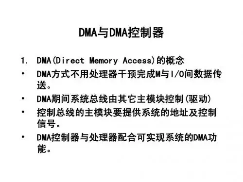
1、直接存储器存取(DMA)⽤来提供在外设和存储器之间或者存储器和存储器之间的⾼速数据传输。
2、⽆须CPU⼲预,数据可以通过DMA快速移动,这就节省了CPU的资源来做其他操作。
3、两个DMA控制器有12个通道(DMA1有7个通道,DMA2有5个通道),每个通道专门⽤来管理来⾃⼀个或者多个外设对存储器访问的请求。
4、还有⼀个冲裁器协调各个DMA请求的优先权。
在同⼀个DMA模块上,多个请求间的优先权可以通过软件编程设置(共有四级:很⾼、⾼、中和低),优先权设置相等时由硬件决定(请求0优先请求1,)5、每个通道都有三个事件标志(DMA半传输、DMA传输完成和DMA传输出错),这三个事件标志逻辑或成为⼀个单独的中断请求。
6、闪存、SRAM、外设的SRAM、APB1、APB2和AHB外设均可作为访问的源和⽬标。
7、可编程的数据传输数⽬:最⼤为655358、如果外设要想通过DMA 来传输数据,必须先给DMA 控制器发送DMA 请求,DMA 收到请求信号之后,控制器会给外设⼀个应答信号,当外设应答后且DMA 控制器收到应答信号之后,就会启动DMA 的传输,直到传输完毕。
DMA 有DMA1 和DMA2 两个控制器,DMA1 有7个通道,DMA2有5 个通道,不同的DMA 控制器的通道对应着不同的外设请求,这决定了我们在软件编程上该怎么设置,具体见DMA 请求映像表。
9、仲裁器当发⽣多个DMA 通道请求时,就意味着有先后响应处理的顺序问题,这个就由仲裁器也管理。
仲裁器管理DMA 通道请求分为两个阶段。
第⼀阶段属于软件阶段,可以在DMA_CCRx 寄存器中设置,有4 个等级:⾮常⾼、⾼、中和低四个优先级。
第⼆阶段属于硬件阶段,如果两个或以上的DMA通道请求设置的优先级⼀样,则他们优先级取决于通道编号,编号越低优先权越⾼,⽐如通道0 ⾼于通道1。
C on f i d e n t i al A20DMA 开发说明V1.02013-03-15C on f i d e n t ia l Revision HistoryVersionDate Changes compared to previous issue v1.02013-03-15初建版本C o n f i d e n t i al 目录1.概述-------------------------------------------------------------------------------------------------------51.1.编写目的----------------------------------------------------------------------------------------51.2.适用范围----------------------------------------------------------------------------------------51.3.相关人员----------------------------------------------------------------------------------------52.模块介绍-------------------------------------------------------------------------------------------------62.1.模块功能介绍----------------------------------------------------------------------------------62.2.相关术语介绍----------------------------------------------------------------------------------62.2.1.DMA--------------------------------------------------------------------------------------62.2.2.描述符(des)-----------------------------------------------------------------------------62.2.3.散列传输--------------------------------------------------------------------------------62.3.模块配置介绍----------------------------------------------------------------------------------62.4.源码结构介绍----------------------------------------------------------------------------------63.模块体系结构描述------------------------------------------------------------------------------------73.1.DMA 驱动架构图------------------------------------------------------------------------------73.2.DMA 软件状态---------------------------------------------------------------------------------74.模块数据结构描述------------------------------------------------------------------------------------94.1.dma_channel_t-----------------------------------------------------------------------------------94.2.cofig_des_t---------------------------------------------------------------------------------------94.3.des_item-----------------------------------------------------------------------------------------104.4.chan_state_e------------------------------------------------------------------------------------104.5.dma_cb_t----------------------------------------------------------------------------------------104.6.dma_op_type_e--------------------------------------------------------------------------------105.模块接口描述-----------------------------------------------------------------------------------------125.1.sw_dma_request-------------------------------------------------------------------------------125.2.sw_dma_release--------------------------------------------------------------------------------125.3.sw_dma_ctl-------------------------------------------------------------------------------------125.4.sw_dma_config--------------------------------------------------------------------------------135.5.sw_dma_enqueue------------------------------------------------------------------------------135.6.sw_dma_getposition---------------------------------------------------------------------------145.7.sw_dma_dump_chan--------------------------------------------------------------------------146.模块开发DEMO-------------------------------------------------------------------------------------156.1.DMA 使用流程图-----------------------------------------------------------------------------156.2.demo 程序--------------------------------------------------------------------------------------156.2.1.test_case_normal.c--------------------------------------------------------------------156.2.2.test_case_normal.h--------------------------------------------------------------------236.2.3.sun7i_dma_test.h----------------------------------------------------------------------246.2.4.sun7i_dma_test.c----------------------------------------------------------------------257.Android 系统支持-------------------------------------------------------------------------------------318.模块调试-----------------------------------------------------------------------------------------------328.1.menuconfig 的配置---------------------------------------------------------------------------32C on f i d e n t i al 8.2.测试用例选择---------------------------------------------------------------------------------328.3.测试操作步骤---------------------------------------------------------------------------------339.总结-----------------------------------------------------------------------------------------------------3410.Declaration--------------------------------------------------------------------------------------------35C on f i d e n t i al 1.概述1.1.编写目的介绍DMA 模块使用方法。
adc dma 回调函数ADC和DMA是嵌入式系统中常用的两个模块,它们在数据采集和传输过程中起着重要的作用。
而回调函数是用来处理异步事件的一种机制。
本文将围绕着ADC、DMA和回调函数展开,详细介绍它们的原理和应用。
我们来了解一下ADC(Analog-to-Digital Converter)模块。
ADC 是一种将模拟信号转换为数字信号的电路,常用于嵌入式系统中对模拟量的采集。
在嵌入式系统中,ADC通常连接着各种传感器,用于采集温度、光照、压力等模拟量信号。
ADC的工作原理是将模拟信号通过采样和量化的方式转换为数字信号,然后再经过处理和分析得到需要的信息。
接下来,我们来介绍DMA(Direct Memory Access)模块。
DMA是一种无需CPU干预就能进行数据传输的技术。
在传统的数据传输方式中,数据需要经过CPU的中转,才能从外设传输到内存或者从内存传输到外设。
而DMA的出现,使得数据传输可以直接在外设和内存之间进行,大大提高了数据传输的效率和速度。
DMA模块中有多个通道,可以同时处理多个数据传输请求,从而实现并行传输。
ADC和DMA常常结合使用,以实现高效的数据采集和传输。
ADC采集的数据可以直接通过DMA传输到内存,而不需要CPU的干预。
这样可以减少CPU的负担,提高系统的响应速度。
在这个过程中,回调函数起到了关键的作用。
回调函数是一种异步事件处理的机制。
在ADC和DMA的数据传输过程中,当数据传输完成或者出现错误时,会触发相应的中断事件。
此时,系统会调用预先注册的回调函数来处理这些事件。
回调函数可以根据具体的需求,进行数据处理、错误处理或者其他操作。
通过回调函数的灵活应用,可以实现更加复杂和高效的系统功能。
在使用ADC和DMA的过程中,编写回调函数需要注意一些细节。
首先,回调函数应该尽量简洁和高效,避免耗费过多的系统资源。
其次,回调函数应该及时处理事件,以免影响系统的实时性。
此外,回调函数还需要考虑异常情况的处理,例如数据溢出、传输错误等。
1DMA简介1.1DMA模块基本特征1)6个DMA通道,都具有独立的PIE中断,对应INT7中断线的1~6分组;2)外设触发源可关联多个外设触发;a.ADC排序器1和排序器2;b.多路缓冲串行端口A和B的发送与接收;c.外部中断XINT1~XINT13d.CPU定时/计数器e.Epwm1~6 ADCSOCA和ADCSOCB信号f.软件触;3)数据源/目的地a.L4~L7 16K*16的SARAM存储器;b.所有XINTF区域(外扩的存储器)c.ADC的结果寄存器d.McBSP-A和McBSP-B的发送和接收缓冲器e.Epwm1~6/HRPWM1~6外设第3帧映射寄存4)字长a.16位或32位字长(McBSP仅限于16位)b.读写操作:4周期/字(对于McBSP 5周期/字)1.2DMA模块触发机制每个DMA通道均有如下的结构框图:1)通过各通道的DMA模块寄存器MODE的外设中断触发选择位PERINTSEL来选择DMA通道的中断触发源;2)使能各通道的DMA模式寄存器MODE的外设中断触发使能位PERINTE,开启外设中断信号触发DMA功能;3)使能各通道的DMA控制寄存器CONTROL的运行状态为RUNSTS,使能该通道并允许接收外设中断触发信号;4)配置完成后,该DMA通道可以能进行数据传输;5)也可调过中断触发源直接通过软件触发DMA,通过置位控制寄存器CONTROL的外设中断强制位PERINTFRC来强制触发,同样也可以通过置位控制寄存器的外设中断清除位PERINTCLR来清除挂起的DMA触发;6)控制寄存器的中断触发标志位PERINTFLG被特定的中断触发置位后将一直保持在置位状态,直到状态机的优先逻辑允许该通道进行数据传输,数据传输开始,该标志位被清零;7)在正常的优先级别下,数据传输完成后才会去响应新的中断触发,如果新的中断触发在处于挂起状态(即未被执行)的情况下又来了一个新的中断触发,此时控制寄存器的溢出标志位OVRFLG会被置位。
verilog dma原理-概述说明以及解释1.引言1.1 概述概述部分的内容可以简要介绍DMA的基本概念和作用,以及本文将要讨论的内容和结构。
概述部分内容示例:概述DMA(Direct Memory Access,直接内存访问)是一种计算机技术,用于实现数据在外设和内存之间的直接传输,不需要CPU的介入。
通过使用DMA,可以提高数据传输的速度和效率,减少CPU的负载,提升系统的整体性能。
本文将介绍DMA的原理及其在Verilog中的实现。
首先,我们将简要介绍DMA的基本概念和作用,以及Verilog语言的基础知识。
然后,我们将详细探讨DMA在Verilog中的实现原理,并分析其在实际应用中的优势和不足之处。
最后,我们将对DMA的应用前景进行展望,并对本文进行总结。
通过阅读本文,读者将深入了解DMA技术的原理和Verilog语言的应用。
同时,读者也将了解DMA在各种应用场景中的潜力和限制,有助于更好地应用它来提升系统性能。
让我们开始探索DMA的奥秘吧!1.2 文章结构文章结构部分的内容:本文将按照以下结构组织和呈现关于Verilog DMA原理的详细资料。
引言部分将首先对Verilog DMA原理进行概述。
我们将简要介绍DMA的基本概念,解释Verilog语言的重要性,并说明本文的目的。
正文部分将进一步深入探讨Verilog DMA在硬件设计中的实现原理。
我们将讨论DMA在Verilog中的具体应用,介绍Verilog语言的特点和用法,以及具体实现DMA的方法和技巧。
结论部分将对Verilog DMA的应用前景进行展望。
我们将评估DMA 在硬件设计中的优势和不足,并总结文章中的观点和结论。
通过以上结构的安排,本文将对读者提供一个全面而深入的Verilog DMA原理的学习资料。
读者将了解到DMA的基本概念和Verilog语言的关键知识,以及如何在Verilog中实现DMA的方法。
同时,我们还会探讨DMA在硬件设计中的前景,并评估其在实际应用中的优势与不足。
第5章DSP接口与总线5.3.1 DMA模块总线结构DMA是基于事件的模块,因此需要有一个外设中断触发才开始DMA数据传输。
6个DMA通道的中断触发源可以独立配置,并且每一个通道都拥有各自独立的PIE中断,当DMA传送开始或结束时,可通过PIE中断告知CPU。
6个通道中,有5个通道具有相同的性能,而通道1具有一个附加特性:其优先级可以配置成比其它通道的优先级高。
DMA 模块的核心是一状态机并与地址控制逻辑总线联系在一起。
正是这个地址控制逻辑总线允许对传输过程中的数据块包括缓冲器间的“乒—乓”数据重新排列。
1.DMA的基本特征具有独立PIE中断的6个通道。
外设中断触发源:ADC排序器1和2、多通道缓冲串口A和B(McBSP-A,McBSP-B)的发送和接收、XINT1~7和XINT13、CPU定时器、ePWM1~6的ADSOCA和ADSOCB 信号以及软件强制触发。
数据源/目的:L4~L7 16K SARAM、所有XINT区域、ADC存储器总线映射结果寄存器、McBSP-A和McBSP-B发送和接收缓冲器、ePWM1~6/HRPWM1~6外设帧3映射的寄存器。
字长度:16位或32位(McBSPs限制为16位)。
吞吐量:4个时钟周期/字(对于McBSP读操作,5个时钟周期/字)。
图5‐17 DMA 结构图图5-17给出了DMA的结构框图。
2. 外设中断事件触发源外设中断事件触发器可以为每个DMA通道独立配置18个触发源中的一个。
在这些中断触发源中,有8个外部中断信号,这些信号可以连接到GPIO引脚上,这就大大增加了触发事件的灵活性。
每个通道MODE寄存器中的PERINTSEL位用来选择该通道的中断触发源。
一个有效的外设中断触发事件将锁存至CONTROL寄存器的PERINTFLG位,并且如果相应的中断和DMA通道被使能(MODE.CHx[PERINTE]和CONTROL.CHx[RUNSTS]位),则DMA通道将会响应中断事件。
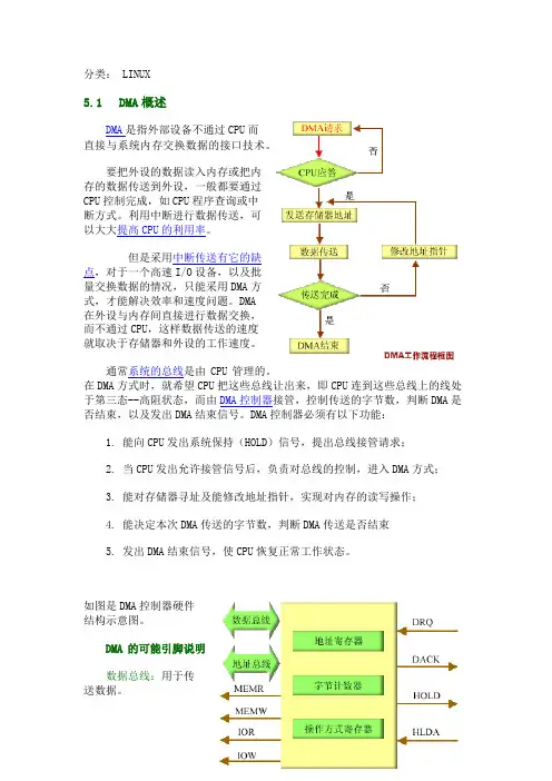
分类: LINUX5.1DMA概述DMA是指外部设备不通过CPU而直接与系统内存交换数据的接口技术。
要把外设的数据读入内存或把内存的数据传送到外设,一般都要通过CPU控制完成,如CPU程序查询或中断方式。
利用中断进行数据传送,可以大大提高CPU的利用率。
但是采用中断传送有它的缺点,对于一个高速I/O设备,以及批量交换数据的情况,只能采用DMA方式,才能解决效率和速度问题。
DMA在外设与内存间直接进行数据交换,而不通过CPU,这样数据传送的速度就取决于存储器和外设的工作速度。
通常系统的总线是由CPU管理的。
在DMA方式时,就希望CPU把这些总线让出来,即CPU连到这些总线上的线处于第三态--高阻状态,而由DMA控制器接管,控制传送的字节数,判断DMA是否结束,以及发出DMA结束信号。
DMA控制器必须有以下功能:1. 能向CPU发出系统保持(HOLD)信号,提出总线接管请求;2. 当CPU发出允许接管信号后,负责对总线的控制,进入DMA方式;3. 能对存储器寻址及能修改地址指针,实现对内存的读写操作;4. 能决定本次DMA传送的字节数,判断DMA传送是否结束5. 发出DMA结束信号,使CPU恢复正常工作状态。
如图是DMA控制器硬件结构示意图。
DMA的可能引脚说明:数据总线:用于传送数据。
地址总线:用于选择存储器地址。
数据传送信号:MEMR为存储器读操作信号,MEMW为存储器写操作信号,IOR为外设读操作信号,IOW为外设写操作信号。
DRQ:DMA请求信号。
是外设向DMA控制器提出要求DMA操作的申请信号。
DACK:DMA响应信号。
是DMA控制器向提出DMA请求的外设表示已收到请求和正进行处理的信号。
HOLD:总线请求信号。
是DMA控制器向CPU要求让出总线的请求信号。
HLDA:总线响应信号,是CPU向DMA控制器表示允许总线请求的应答信号。
5.2DMA工作方式随着大规模集成电路技术的发展,DMA传送已不局限于存储器与外设间的信息交换,而可以扩展为在存储器的两个区域之间,或两种高速的外设之间进行DMA传送,如图所示。
TMS320x2833x,2823x Direct Memory Access (DMA)ModuleReference GuideLiterature Number:SPRUFB8DSeptember2007–Revised April20112SPRUFB8D–September2007–Revised April2011Submit Documentation FeedbackPreface (6)1Introduction (8)2Architecture (10)2.1Block Diagram (10)2.2Peripheral Interrupt Event Trigger Sources (10)2.3DMA Bus (13)3Pipeline Timing and Throughput (13)4CPU Arbitration (15)4.1For the External Memory Interface(XINTF)Zones (15)4.2For All Other Peripherals/Memories (16)5Channel Priority (16)5.1Round-Robin Mode (16)5.2Channel1High Priority Mode (17)6Address Pointer and Transfer Control (17)7ADC Sync Feature (22)8Overrun Detection Feature (24)9Register Descriptions (25)9.1DMA Control Register(DMACTRL)—EALLOW Protected (26)9.2Debug Control Register(DEBUGCTRL)—EALLOW Protected (27)9.3Revision Register(REVISION) (27)9.4Priority Control Register1(PRIORITYCTRL1)—EALLOW Protected (28)9.5Priority Status Register(PRIORITYSTAT) (29)9.6Mode Register(MODE)—EALLOW Protected (30)9.7Control Register(CONTROL)—EALLOW Protected (32)9.8Burst Size Register(BURST_SIZE)—EALLOW Protected (34)9.9BURST_COUNT Register (34)9.10Source Burst Step Register Size(SRC_BURST_STEP)—EALLOW Protected (35)9.11Destination Burst Step Register Size(DST_BURST_STEP)—EALLOW Protected (36)9.12Transfer Size Register(TRANSFER_SIZE)—EALLOW Protected (36)9.13Transfer Count Register(TRANSFER_COUNT) (37)9.14Source Transfer Step Size Register(SRC_TRANSFER_STEP)—EALLOW Protected (37)9.15Destination Transfer Step Size Register(DST_TRANSFER_STEP)—EALLOW Protected (38)9.16Source/Destination Wrap Size Register(SRC/DST_WRAP_SIZE)—EALLOW protected) (38)9.17Source/Destination Wrap Count Register(SCR/DST_WRAP_COUNT) (39)9.18Source/Destination Wrap Step Size Registers(SRC/DST_WRAP_STEP)—EALLOW Protected (39)9.19Shadow Source Begin and Current Address Pointer Registers(SRC_BEG_ADDR_SHADOW/DST_BEG_ADDR_SHADOW)—All EALLOW Protected (40)9.20Active Source Begin and Current Address Pointer Registers(SRC_BEG_ADDR/DST_BEG_ADDR) (40)9.21Shadow Destination Begin and Current Address Pointer Registers(SRC_ADDR_SHADOW/DST_ADDR_SHADOW)—All EALLOW Protected (41)9.22Active Destination Begin and Current Address Pointer Registers(SRC_ADDR/DST_ADDR) (41)Appendix A Revision History (42)3 SPRUFB8D–September2007–Revised April2011Table of Contents Submit Documentation FeedbackList of Figures1DMA Block Diagram (10)2Peripheral Interrupt Trigger Input Diagram (12)34-Stage Pipeline DMA Transfer (13)44-Stage Pipeline With One Read Stall(McBSP as source) (14)5DMA State Diagram (21)6ADC Sync Input Diagram (23)7Overrun Detection Logic (24)8DMA Control Register(DMACTRL) (26)9Debug Control Register(DEBUGCTRL) (27)10Revision Register(REVISION) (27)11Priority Control Register1(PRIORITYCTRL1) (28)12Priority Status Register(PRIORITYSTAT) (29)13Mode Register(MODE) (30)14Control Register(CONTROL) (32)15Burst Size Register(BURST_SIZE) (34)16Burst Count Register(BURST_COUNT) (34)17Source Burst Step Size Register(SRC_BURST_STEP) (35)18Destination Burst Step Register Size(DST_BURST_STEP) (36)19Transfer Size Register(TRANSFER_SIZE) (36)20Transfer Count Register(TRANSFER_COUNT) (37)21Source Transfer Step Size Register(SRC_TRANSFER_STEP) (37)22Destination Transfer Step Size Register(DST_TRANSFER_STEP) (38)23Source/Destination Wrap Size Register(SRC/DST_WRAP_SIZE) (38)24Source/Destination Wrap Count Register(SCR/DST_WRAP_COUNT) (39)25Source/Destination Wrap Step Size Registers(SRC/DST_WRAP_STEP) (39)26Shadow Source Begin and Current Address Pointer Registers(SRC_BEG_ADDR_SHADOW/DST_BEG_ADDR_SHADOW) (40)27Active Source Begin and Current Address Pointer Registers(SRC_BEG_ADDR/DST_BEG_ADDR) (40)28Shadow Destination Begin and Current Address Pointer Registers(SRC_ADDR_SHADOW/DST_ADDR_SHADOW) (41)29Active Destination Begin and Current Address Pointer Registers(SRC_ADDR/DST_ADDR) (41)4List of Figures SPRUFB8D–September2007–Revised April2011Submit Documentation FeedbackList of Tables1Peripheral Interrupt Trigger Source Options (12)2DMA Register Summary (25)3DMA Control Register(DMACTRL)Field Descriptions (26)4Debug Control Register(DEBUGCTRL)Field Descriptions (27)5Revision Register(REVISION)Field Descriptions (27)6Priority Control Register1(PRIORITYCTRL1)Field Descriptions (28)7Priority Status Register(PRIORITYSTAT)Field Descriptions (29)8Mode Register(MODE)Field Descriptions (30)9Control Register(CONTROL)Field Descriptions (32)10Burst Size Register(BURST_SIZE)Field Descriptions (34)11Burst Count Register(BURST_COUNT)Field Descriptions (34)12Source Burst Step Size Register(SRC_BURST_STEP)Field Descriptions (35)13Destination Burst Step Register Size(DST_BURST_STEP)Field Descriptions (36)14Transfer Size Register(TRANSFER_SIZE)Field Descriptions (36)15Transfer Count Register(TRANSFER_COUNT)Field Descriptions (37)16Source Transfer Step Size Register(SRC_TRANSFER_STEP)Field Descriptions (37)17Destination Transfer Step Size Register(DST_TRANSFER_STEP)Field Descriptions (38)18Source/Destination Wrap Size Register(SRC/DST_WRAP_SIZE)Field Descriptions (38)19Source/Destination Wrap Count Register(SCR/DST_WRAP_COUNT)Field Descriptions (39)20Source/Destination Wrap Step Size Registers(SRC/DST_WRAP_STEP)Field Descriptions (39)21Shadow Source Begin and Current Address Pointer Registers(SRC_BEG_ADDR_SHADOW/DST_BEG_ADDR_SHADOW)Field Descriptions (40)22Active Source Begin and Current Address Pointer Registers(SRC_BEG_ADDR/DST_BEG_ADDR)Field Descriptions (40)23Shadow Destination Begin and Current Address Pointer Registers(SRC_ADDR_SHADOW/DST_ADDR_SHADOW)Field Descriptions (41)24Active Destination Begin and Current Address Pointer Registers(SRC_ADDR/DST_ADDR)Field Descriptions (41)25Document Revision History (42)5 SPRUFB8D–September2007–Revised April2011List of Tables Submit Documentation FeedbackPrefaceSPRUFB8D–September2007–Revised April2011Read This First The DMA module described in this reference guide is a Type0DMA.See the TMS320C28xx,28xxx DSP Peripheral Reference Guide(SPRU566)for a list of all devices with a DMA module of the same type,to determine the differences between the types,and for a list of device-specific differences within a type.Notational ConventionsThis document uses the following conventions.•Hexadecimal numbers are shown with the suffix h or with a leading0x.For example,the following number is40hexadecimal(decimal64):40h or0x40.•Registers in this document are shown in figures and described in tables.–Each register figure shows a rectangle divided into fields that represent the fields of the register.Each field is labeled with its bit name,its beginning and ending bit numbers above,and itsread/write properties below.A legend explains the notation used for the properties.–Reserved bits in a register figure designate a bit that is used for future device expansion.Related DocsThe following documents support the2833x and2823x devices and can be downloaded from the Texas Instruments web site:.Data Manual and Errata—SPRS439—TMS320F28335,TMS320F28334,TMS320F28332,TMS320F28235,TMS320F28234, TMS320F28232Digital Signal Controllers(DSCs)Data Manual contains the pinout,signaldescriptions,as well as electrical and timing specifications for the F2833x/2823x devices.SPRZ272—TMS320F28335,F28334,F28332,TMS320F28235,F28234,F28232Digital Signal Controllers(DSCs)Silicon Errata describes the advisories and usage notes for different versions ofsilicon.CPU User's Guides—SPRU430—TMS320C28x CPU and Instruction Set Reference Guide describes the central processing unit(CPU)and the assembly language instructions of the TMS320C28x fixed-point digital signalprocessors(DSPs).It also describes emulation features available on these DSPs.SPRUEO2—TMS320C28x Floating Point Unit and Instruction Set Reference Guide describes the floating-point unit and includes the instructions for the FPU.Peripheral Guides—SPRU566—TMS320x28xx,28xxx DSP Peripheral Reference Guide describes the peripheral reference guides of the28x digital signal processors(DSPs).SPRUFB0—TMS320x2833x,2823x System Control and Interrupts Reference Guide describes the various interrupts and system control features of the2833x and2823x digital signal controllers(DSCs).SPRU812—TMS320x2833x,2823x Analog-to-Digital Converter(ADC)Reference Guide describes how to configure and use the on-chip ADC module,which is a12-bit pipelined ADC.SPRU949—TMS320x2833x,2823x DSC External Interface(XINTF)Reference Guide describes the XINTF,which is a nonmultiplexed asynchronous bus,as it is used on the2833x and2823x devices.6Preface SPRUFB8D–September2007–Revised April2011Submit Documentation Feedback Related Docs SPRU963—TMS320x2833x,2823x Boot ROM Reference Guide describes the purpose and features of the bootloader(factory-programmed boot-loading software)and provides examples of code.It alsodescribes other contents of the device on-chip boot ROM and identifies where all of the informationis located within that memory.SPRUFB7—TMS320x2833x,2823x Multichannel Buffered Serial Port(McBSP)Reference Guide describes the McBSP available on the2833x and2823x devices.The McBSPs allow directinterface between a DSP and other devices in a system.SPRUFB8—TMS320x2833x,2823x Direct Memory Access(DMA)Module Reference Guide describes the DMA on the2833x and2823x devices.SPRUG04—TMS320x2833x,2823x Enhanced Pulse Width Modulator(ePWM)Module Reference Guide describes the main areas of the enhanced pulse width modulator that include digital motorcontrol,switch mode power supply control,UPS(uninterruptible power supplies),and other forms ofpower conversion.SPRUG02—TMS320x2833x,2823x High-Resolution Pulse Width Modulator(HRPWM)Reference Guide describes the operation of the high-resolution extension to the pulse width modulator(HRPWM).SPRUFG4—TMS320x2833x,2823x Enhanced Capture(eCAP)Module Reference Guide describes the enhanced capture module.It includes the module description and registers.SPRUG05—TMS320x2833x,2823x Enhanced Quadrature Encoder Pulse(eQEP)Module Reference Guide describes the eQEP module,which is used for interfacing with a linear or rotaryincremental encoder to get position,direction,and speed information from a rotating machine inhigh-performance motion and position control systems.It includes the module description andregisters.SPRUEU1—TMS320x2833x,2823x Enhanced Controller Area Network(eCAN)Reference Guide describes the eCAN that uses established protocol to communicate serially with other controllers inelectrically noisy environments.SPRUFZ5—TMS320x2833x,2823x Serial Communications Interface(SCI)Reference Guide describes the SCI,which is a two-wire asynchronous serial port,commonly known as a UART.TheSCI modules support digital communications between the CPU and other asynchronous peripheralsthat use the standard non-return-to-zero(NRZ)format.SPRUEU3—TMS320x2833x,2823x DSC Serial Peripheral Interface(SPI)Reference Guide describes the SPI-a high-speed synchronous serial input/output(I/O)port-that allows a serial bitstream of programmed length(one to sixteen bits)to be shifted into and out of the device at aprogrammed bit-transfer rate.SPRUG03—TMS320x2833x,2823x Inter-Integrated Circuit(I2C)Module Reference Guide describes the features and operation of the inter-integrated circuit(I2C)module.Tools Guides—SPRU513—TMS320C28x Assembly Language Tools v5.0.0User's Guide describes the assembly language tools(assembler and other tools used to develop assembly language code),assemblerdirectives,macros,common object file format,and symbolic debugging directives for theTMS320C28x device.SPRU514—TMS320C28x Optimizing C/C++Compiler v5.0.0User's Guide describes the TMS320C28x™C/C++compiler.This compiler accepts ANSI standard C/C++source code andproduces TMS320DSP assembly language source code for the TMS320C28x device.SPRU608—TMS320C28x Instruction Set Simulator Technical Overview describes the simulator, available within the Code Composer Studio for TMS320C2000IDE,that simulates the instructionset of the C28x™core.SPRU625—TMS320C28x DSP/BIOS5.32Application Programming Interface(API)Reference Guide describes development using DSP/BIOS.7 SPRUFB8D–September2007–Revised April2011Read This First Submit Documentation FeedbackReference GuideSPRUFB8D–September2007–Revised April2011 TMS320x2833x Direct Memory Access(DMA)ModuleThe direct memory access(DMA)module provides a hardware method of transferring data between peripherals and/or memory without intervention from the CPU,thereby freeing up bandwidth for other system functions.Additionally,the DMA has the capability to orthogonally rearrange the data as it is transferred as well as“ping-pong”data between buffers.These features are useful for structuring data into blocks for optimal CPU processing.1IntroductionThe strength of a digital signal controller(DSC)is not measured purely in processor speed,but in total system capabilities.As a part of the equation,any time the CPU bandwidth for a given function can be reduced,the greater the system capabilities.Many times applications spend a significant amount of their bandwidth moving data,whether it is from off-chip memory to on-chip memory,or from a peripheral such as an analog-to-digital converter(ADC)to RAM,or even from one peripheral to another.Furthermore,many times this data comes in a format that is not conducive to the optimum processing powers of the CPU.The DMA module described in this reference guide has the ability to free up CPU bandwidth and rearrange the data into a pattern for more streamlined processing.The DMA module is an event-based machine,meaning it requires a peripheral interrupt trigger to start a DMA transfer.Although it can be made into a periodic time-driven machine by configuring a timer as the interrupt trigger source,there is no mechanism within the module itself to start memory transfersperiodically.The interrupt trigger source for each of the six DMA channels can be configured separately and each channel contains its own independent PIE interrupt to let the CPU know when a DMA transfers has either started or completed.Five of the six channels are exactly the same,while Channel1has one additional feature:the ability to be configured at a higher priority than the others.At the heart of the DMA is a state machine and tightly coupled address control logic.It is this address control logic that allows for rearrangement of the block of data during the transfer as well as the process of ping-ponging databetween buffers.Each of these features,along with others will be discussed in detail in this document.DMA Overview:•6channels with independent PIE interrupts•Peripheral interrupt trigger sources–ADC sequencer1and sequencer2–Multichannel Buffered Serial Port A and B(McBSP-A,McBSP-B)transmit and receive–XINT1-7and XINT13–CPU Timers–ePWM1-6ADCSOCA and ADSOCB signals–Software•Data sources/destinations:–L4-L716K x16SARAM–All XINTF zones–ADC memory bus mapped result registers–McBSP-A and McBSP-B transmit and receive buffers–ePWM1-6/HRPWM1-6Peripheral Frame3mapped registers•Word Size:16-bit or32-bit(McBSPs limited to16-bit)•Throughput:4cycles/word(5cycles/word for McBSP reads)8TMS320x2833x Direct Memory Access(DMA)Module SPRUFB8D–September2007–Revised April2011Submit Documentation Feedback Introduction NOTE:The ePWM/HRPWM are not present on all devices and/or revisions.See the TMS320x28xx,28xxx DSP Peripheral Reference Guide(SPRU566)for specifics.9 SPRUFB8D–September2007–Revised April2011TMS320x2833x Direct Memory Access(DMA)Module Submit Documentation FeedbackArchitecture 2Architecture2.1Block DiagramFigure1shows a device level block diagram of the DMA.Figure1.DMA Block DiagramA The ePWM/HRPWM registers must be remapped to PF3(through bit0of the MAPCNF register)before they can beaccessed by the DMA.The ePWM/HRPWM connection to DMA is not present in silicon revision0.2.2Peripheral Interrupt Event Trigger SourcesThe peripheral interrupt event trigger can be independently configured as one of eighteen differentsources for each of the six DMA channels.Included in these sources are8external interrupt signals which can be connected to most of the general-purpose input/output(GPIO)pins on the device.This addssignificant flexibility to the event trigger capabilities.A bit field called PERINTSEL in the MODE register of each channel is used to select that channels interrupt trigger source.An active peripheral interrupt trigger will be latched into the PERINTFLG bit of the CONTROL register,and if the respective interrupt and DMA channel is enabled(see the MODE.CHx[PERINTE]and CONTROL.CHx[RUNSTS]bits),it will be serviced by the DMA channel.Upon receipt of a peripheral interrupt event signal,the DMA will automatically send a clear signal to the interrupt source so that subsequent interrupt events will occur.Regardless of the value of the MODE.CHx[PERINTSEL]bit field,software can always force a trigger by using the CONTROL.CHx[PERINTFRC]bit.Likewise,software can always clear a pending DMA trigger using the CONTROL.CHx[PERINTCLR]bit.10TMS320x2833x Direct Memory Access(DMA)Module SPRUFB8D–September2007–Revised April2011Submit Documentation Feedback Architecture Once a particular interrupt trigger sets a channel’s PERINTFLG bit,the bit stays pending until the priority logic of the state machine starts the burst transfer for that channel.Once the burst transfer starts,the flag is cleared.If a new interrupt trigger is generated while a burst is in progress,the burst will complete before responding to the new interrupt trigger(after proper prioritization).If a third interrupt trigger occurs before the pending interrupt is serviced,an error flag is set in the CONTROL.CHx[OVRFLG]bit.If a peripheral interrupt trigger occurs at the same time as the latched flag is being cleared,the peripheral interrupttrigger has priority and the PERINTFLG will remain set.Figure2shows a diagram of the trigger select circuit.See the MODE.CHx[PERINTSEL]bit fielddescription for the complete list of peripheral interrupt trigger sources.11 SPRUFB8D–September2007–Revised April2011TMS320x2833x Direct Memory Access(DMA)Module Submit Documentation FeedbackNoneSEQ1INT SEQ2INT EPWM5SOCBEPWM6SOCA EPWM6SOCB...Architecture Figure 2.Peripheral Interrupt Trigger Input DiagramTable 1shows the interrupt trigger source options that are available for each channel.Table 1.Peripheral Interrupt Trigger Source OptionsPeripheralInterrupt Trigger Source CPUDMA Software bit (CHx.CONTROL.PERINTFRC)only ADCSequencer 1Interrupt Sequencer 2Interrupt External Interrupts External Interrupt 1External Interrupt 2External Interrupt 3External Interrupt 4External Interrupt 5External Interrupt 6External Interrupt 7External Interrupt 13CPU Timers Timer 0OverflowTimer 1OverflowTimer 2OverflowMcBSP-AMcBSP-A Transmit Buffer Empty McBSP-A Receive Buffer Full McBSP-BMcBSP-B Transmit Buffer Empty McBSP-B Receive Buffer Full ePWM1(1)ADC Start of Conversion A ADC Start of Conversion B ePWM2(1)ADC Start of Conversion AADC Start of Conversion BePWM3(1)ADC Start of Conversion A (1)The ePWM1-6are not present on all devices and/or revisions.Seethe TMS320x28xx,28xxx DSP Peripheral Reference Guide(SPRU566)for specifics.12TMS320x2833x Direct Memory Access (DMA)ModuleSPRUFB8D–September 2007–Revised April 2011Submit Documentation FeedbackSYSCLKAddr bus Data bus Generate address Pipeline Timing and ThroughputTable 1.Peripheral Interrupt Trigger Source Options(continued)PeripheralInterrupt Trigger Source ADC Start of Conversion B ePWM4(1)ADC Start of Conversion A ADC Start of Conversion B ePWM5(1)ADC Start of Conversion A ADC Start of Conversion B ePWM6(1)ADC Start of Conversion AADC Start of Conversion B2.3DMA BusThe DMA bus architecture consists of a 22-bit address bus,a 32-bit data read bus,and a 32-bit data write bus.Memories and register locations connected to the DMA bus are via interfaces that sometimes share resources with the CPU memory or peripheral bus.Arbitration rules are defined in Section 4.The following resources are connected to the DMA bus:•XINTF Zones 0,6&7•L4SARAM•L5SARAM•L6SARAM•L7SARAM•ADC Memory Mapped Result Registers•McBSP-A and McBSP-B Data Receive Registers (DRR2/DRR1)and Data Transmit Registers(DXR2/DXR1)•ePWM1-6/HRPWM1-6Register when mapped to Peripheral Frame 33Pipeline Timing and ThroughputThe DMA consists of a 4-stage pipeline as shown in Figure 3.The one exception to this is when a DMA channel is configured to have one of the McBSPs as its data source.A read of a McBSP DRR register stalls the DMA bus for one cycle during the read portion of the transfer,as shown in Figure 4.Figure 3.4-Stage Pipeline DMA Transfer13SPRUFB8D–September 2007–Revised April 2011TMS320x2833x Direct Memory Access (DMA)Module Submit Documentation FeedbackSYSCLKAddr bus Data bus Generate addressPipeline Timing and Throughput Figure 4.4-Stage Pipeline With One Read Stall (McBSP as source)14TMS320x2833x Direct Memory Access (DMA)Module SPRUFB8D–September 2007–Revised April 2011Submit Documentation Feedback CPU ArbitrationIn addition to the pipeline there are a few other behaviors of the DMA that affect it’s total throughput•A1-cycle delay is added at the beginning of each burst•A1-cycle delay is added when returning from a CH1high priority interrupt•32-bit transfers run at double the speed of a16-bit transfer(i.e.,it takes the same amount of time to transfer a32-bit word as it does a16-bit word)•Collisions with the CPU may add delay slots(see Section4)For example,to transfer12816-bit words from ADC to RAM a channel can be configured to transfer8 bursts of16words/burst.This will give:8bursts*[(4cycles/word*16words/burst)+1]=520cyclesIf instead the channel were configured to transfer the same amount of data32bits at a time(the word size is configured to32bits)the transfer would take:8bursts*[(4cycles/word*8words/burst)+1]=264cycles4CPU ArbitrationTypically,DMA activity is independent of the CPU activity.Under the circumstance where both the DMA and the CPU are attempting to access memory or a peripheral register within the same interfaceconcurrently,an arbitration procedure will occur.The one exception is with the memory mapped(PF0) ADC registers,which do not create a conflict when read by both the CPU and the DMA simultaneously, even if different addresses are accessed.Any combined accesses between the different interfaces,orwhere the CPU access is outside of the interface that the DMA is accessing do not create a conflict.The interfaces which internally contain conflicts are:•XINTF Memory Zones0,6and7•L4RAM•L5RAM•L6RAM•L7RAM•Peripheral Frame3(McBSP-A,McBSP-B,and ePWM1-6/HRPWM1-6)NOTE:The ePWM/HRPWM are not present on all devices and/or revisions.See the TMS320x28xx,28xxx DSP Peripheral Reference Guide(SPRU566)for specifics.4.1For the External Memory Interface(XINTF)Zones•If the CPU and the DMA attempt an access to any of the XINTF zones on the same cycle,the DMA is serviced first,followed by all the pending CPU accesses(in the proper priority order for CPU accesses: write→read→fetch).•If CPU accesses to an XINTF zone are pending or being processed by the XINTF and a DMA access to an XINTF zone is attempted,the DMA access is stalled until all CPU pending accesses arecompleted.For example,if a CPU write and read access is pending and a fetch is in progress,first the fetch is completed,then the CPU write is performed,then the CPU read is performed,and then theDMA access is performed.•There is a1cycle stall if simultaneous write accesses by the CPU and the DMA are attempted.If the DMA or CPU is used to write to the XINTF zones,then the write buffer of the XINTF can help toavoid CPU or DMA stalls.If the CPU or DMA are performing reads from XINTF,then significant stalls can occur.The only concern here is if the DMA is stalled and the DMA misses other higher priority DMAevents such as servicing the ADC which can generate data at a high rate.In such situations,the DMAshould not be used to transfer data on XINTF,if the stalls are too long that there is potential to miss other DMA events.15 SPRUFB8D–September2007–Revised April2011TMS320x2833x Direct Memory Access(DMA)Module Submit Documentation FeedbackChannel Priority The DMA does not support abort mechanisms for DMA reads from XINTF.If the DMA is performing an access to one of the XINTF zones and the DMA access is stalled(XREADY not responding)then the CPU can issue a HARDRESET that would abort the access.HARDRESET behaves like a System Reset on the DMA.Likewise,a HARDRESET needs to be applied to the XINTF hence releasing the peripheral from the struck ready condition.Any data that is write buffered or pending on the XINTF or DMA will be lost.4.2For All Other Peripherals/Memories•If the CPU and the DMA make an access to the same interface in the same cycle,the DMA has priority and the CPU is stalled.•If a CPU access to an interface is in progress and another CPU access to the same interface is pending,for example,the CPU is performing a write operation and a read operation from the CPU ispending,then a DMA access to that same interface has priority over the pending CPU access whenthe current CPU access completes.NOTE:If the CPU is performing a read-modify-write operation and the DMA performs a write to thesame location,the DMA write may be lost if the operation occurs in between the CPU readand the CPU write.For this reason,it is advised not to mix such CPU accesses with DMAaccesses to the same locations.In the case of RAM,a ping-pong scheme can be implemented to avoid the CPU and the DMA accessing the same RAM block concurrently,thus avoiding any stalls or corruption issues.5Channel PriorityTwo priority schemes exist when determining channel priority:Round-robin mode and Channel1high-priority mode.5.1Round-Robin ModeIn this mode,all channels have equal priority and each enabled channel is serviced in round-robin fashion as follows:CH1→CH2→CH3→CH4→CH5→CH6→CH1→CH2→…In the case above,after each channel has transferred a burst of words,the next channel is serviced.You can specify the size of the burst for each channel.Once CH6(or the last enabled channel)has beenserviced,and no other channels are pending,the round-robin state machine enters an idle state.From the idle state,channel1(if enabled)is always serviced first.However,if the DMA is currentlyprocessing another channel x,all other pending channels between x and the end of the round are serviced before CH1.It is in this sense that all the channels are of equal priority.For instance,take an example where CH1,CH4,and CH5are enabled in round-robin mode and CH4is currently being processed.Then CH1and CH5both receive an interrupt trigger from their respective peripherals before CH4completes.CH1and CH5are now both pending.When CH4completes its burst,CH5will be serviced next.Only after CH5completes will CH1be serviced.Upon completion of CH1,if there are no more channels pending,the round-robin state machine will enter an idle state.A more complicated example is shown below:•Assume all channels are enabled,and the DMA is in an idle state,•Initially a trigger occurs on CH1,CH3,and CH5on the same cycle,•When the CH1burst transfer starts,requests from CH3and CH5are pending,•Before completion of the CH1burst,the DMA receives a request from CH2.Now the pending requests are from CH2,CH3,and CH5,•After completing the CH1burst,CH2will be serviced since it is next in the round-robin scheme after CH1.•After the burst from CH2is finished,the CH3burst will be serviced,followed by CH5burst.•Now while the CH5burst is being serviced,the DMA receives a request from CH1,CH3,and CH6.16TMS320x2833x Direct Memory Access(DMA)Module SPRUFB8D–September2007–Revised April2011Submit Documentation Feedback。
DMA相关知识直接存储器访问(DMA)模块是一种不需要CPU干涉而实现外设与内存之间的数据交换的方式。
直接存储器访问就是用硬件实现存储器与存储器之间,存储器与I/O口设备之间进行高速数据传送,极大的提高了批量数据的传送速度。
实现DMA传送的关键部位是DMA控制器(DMAC)。
DMAC和CPU都可以控制系统总线,从而控制总线的发送信息。
但是同一时刻,系统总线只能接受一个部件的控制。
由这两个部件之间的“联络信号”控制实现的。
DMA传送期间,CPU让出总线控制权,这可能影响诸如中断请求的及时响应和处理,同时DMA传送方式的高速度是以增加系统的复杂性和成本为代价的。
DMA模块的核心其实是一个与地址控制逻辑紧密关联的状态机,在数据传输过程中让数据块自动的重新配置,就好像两个缓冲器之间打乒乓球一样,我们把这种机制也叫作DMA的乒乓机制。
一.DMA主要特征如下:1.具有独立中断控制6路DMA通道。
2.可作为DMA传送的触发信号有:●ADC序列发生器1和序列发生器2;●多路缓冲器串口McBSPA和McBSPB的发送和接收;●XINT1~7和XINT13;●CPU定时器;●ePWM1~6,ADCSOCA和ADCSOCB信号;●软件强制;3.数据源及目标:●L4~L7 16K×16位SARAM;●所有XINTF区域;●ADC存储器;●McBSP-A和McBSP-B发送及接收数据缓冲器;●ePWM1~6/HRPWM1~6处在外射单元3的寄存器。
4.字长:16位或32位;5.流量:4周期每字;二.DMA传送过程大致有以下几个步骤:1.当外设输入数据准备好,外设向DMA发出一个选通信号,将数据送到数据端口;向DMA发出请求;2.DMA控制器向CPU发出总线请求信号(HOLD)高电平;3.CPU在现行总线周期结束后响应,向DMA发出响应信号(HLDA)高电平。
4.CPU待该总线周期结束时,放弃对总线控制,DMA控制器接管三态总线,接口将数据送上数据总线,并撤销DMA请求。
DMA操作须知对于进行DMA(直接内存存取)操作的硬件开发人员来说,了解和掌握一些DMA操作的须知是非常重要的。
DMA操作是一种实现设备之间直接数据传输的方式,它可以在不占用CPU时间的情况下完成数据传输任务。
本文将介绍DMA操作的基本原理、操作流程以及一些需要注意的问题。
一、DMA操作的基本原理DMA操作是通过一个特殊的硬件模块来实现的,该硬件模块被称为DMA控制器。
DMA控制器拥有自己的地址总线和数据总线,可以直接和主存、外设进行数据传输,而不需要CPU的介入。
其基本原理如下:1. 初始化:首先,需要对DMA控制器进行初始化设置。
包括设置数据传输的方向(读或写)、传输字节数、源地址和目的地址等参数。
2. 请求传输:DMA控制器向CPU发送传输请求,在CPU确认后,控制权转移到DMA控制器。
3. 寻址:DMA控制器根据设置的地址和字节数,在总线上进行地址寻址,以确定需要传输的数据位置。
4. 数据传输:DMA控制器通过数据总线进行数据传输,将数据读取到缓冲区(或从缓冲区写入到目的地址)。
5. 完成传输:数据传输完成后,DMA控制器会向CPU发送中断请求,以通知CPU传输已完成。
二、DMA操作的流程在进行DMA操作前,需要先进行一些准备工作。
具体的流程如下:1. 设置DMA控制器的参数:包括数据传输的方向、传输字节数、源地址和目的地址等。
这些参数可以根据具体的应用场景进行设置。
2. 初始化数据缓冲区:DMA控制器需要通过读写数据缓冲区来进行数据传输。
在开始DMA操作前,需要先对缓冲区进行初始化,确保数据的准确性。
3. 发送DMA传输请求:DMA控制器向CPU发送传输请求,请求得到CPU的响应后,控制权转移到DMA控制器。
4. 执行DMA传输:DMA控制器根据设置的地址和字节数,通过地址总线和数据总线进行数据传输。
传输完成后,DMA控制器向CPU发送中断请求。
5. 处理中断请求:CPU接收到DMA控制器的中断请求后,会执行相应的中断处理程序,以完成数据的处理和后续操作。
//北京联合大学实训基地潘峰//qq:66797490//微博:潘峰_buu//博客:/panpan_0315/blog/DMA模块DMA模块简介所谓DMA就是直接内存存取(Direct Memory Access),是计算机科学中的一种内存访问技术。
以前我们向内存传送数据,都是通过CPU来进行。
比如AD完成后,我们要把结果寄存器中的值传送到内存的一个变量中,一种方法就是查询COCO标志位(详见ADC模块一节),一旦置1,就读取结果寄存器并传送。
这种方法CPU需要不断查询标志位,耽误时间,降低效率。
我们也可以使用中断的方式,CPU并不需要轮询标志位,而是AD转换完成后触发中断,CPU中断当前的程序,转向执行中断服务程序,在中断服务程序中读取结果寄存器,然后传送到内存中。
这种方式虽然省去了轮询的时间消耗,但传送数据仍然是由CPU完成的,如果是大批量数据高速传输的话,频繁的中断也将造成很重的CPU负担,于是就有了DMA。
和轮询方式、中断方式不同的是,DMA是通过DMA控制器接管数据和地址总线,根据事先设定好的源地址和目的地址,以及传送的字节数,将数据自动传送到指定的位置,而不需要CPU的介入,从而CPU的负担大大减轻。
如果CPU正在执行指令,DMA控制利用空闲的地址和数据总线完成数据传送,某种程度上说,CPU运算和数据传送是在并行进行的。
在制作智能车的应用中,摄像头组的同学,需要将摄像头采集的数据用最快的速度传送到内存变量中,以采集更多的点。
Kinetis芯片的DMA功能这个时候就能发挥重要的作用了。
首先我们需要了解一下和Kinetis芯片的DMA功能有关的一些概念。
1.DMA源和DMA通道在Kinetis芯片中,很多模块都可以请求DMA模块进行数据传送。
所谓DMA源,也就是DMA传送请求是谁发出的。
以K60DN512Z为例,共有63个DMA源。
而DMA源发出的DMA请求并不是直接提交到DMA控制器,而是通过DMA多路复用器的16个DMA通道提交的。
需要设置相关的寄存器建立DMA源和DMA通道之间的映射关系。
如图错误!文档中没有指定样式的文字。
-1所示。
图错误!文档中没有指定样式的文字。
-1 DMA多路复用器2.DMA模块框图DMA控制模块分为两部分,一个是DMA引擎(eDMA Engine)。
一个是DMA传输控制描述符(TCD),如图错误!文档中没有指定样式的文字。
-2所示。
图错误!文档中没有指定样式的文字。
-2 DMA控制框图3.DMA描述符每个通道需要一个32个字节的传输控制描述符用于定义我们想要的数据传送操作。
描述符按通道0~通道15的顺序依次存放在DMA模块的内存中。
描述符中包含了对应的数据传送的所有信息,主要有源地址,目的地址,传送次数,每次传送的字节数,传送完毕后源地址和目的地址如何调整等等,当一个通道的DMA传送结束后,源地址和目的地址需要加上各自的调整量回写到TCD中,传送计数也需要重新初始化并回写到TCD中。
如表错误!4.主循环和副循环数据的传送分为主循环(major loop)和副循环(minor loop)。
如何理解这两个概念呢。
我们不妨假设用软件来实现有规律的顺序数据传送,使用C语言来实现的话,可以用for循环。
好比用两层嵌套的for循环来实现。
如使用DMA做同样的工作,过程是相同的,外层的循环又称主循环,即major loop。
内层循环称为副循环,即minor loop。
major loop 循环一次,可能需要minor loop循环多次。
每个minor loop循环都需要DMA源发来请求或者通过软件请求。
每个minor loop传送完毕,对应的DMA通道就进入空闲模式,等待下一次DMA 请求。
当所有DMA传送完毕,即置DONE标志,并且可以通过设置选择传送完毕是否触发中断。
5.主/副循环链接功能Kinetis的DMA模块有个功能叫主/副循环链接,就是当一个通道的主循环(Major loop)或副循环(minor loop)结束后,自动链接到另一个通道进行传输。
比如你可以用通道0传送AD数据到内存,完毕后,立刻链接到通道1将内存中的数再传送到DAC。
如果要使用这个功能,需要设置DMA_TCDn_CSR寄存器或DMA_TCD_CITER寄存器。
6.散/聚模式Kinetis的DMA模块还有个特殊的功能叫散/聚模式(Scatter/Gather)。
在这个模式下,当一个通道的主循环(major loop)传输结束后,由一个指针指向一个内存中的新的传输控制描述符(TCD)的起始地址,DMA控制器将从内存中载入该描述符。
这种应用可用在分散存储的内存应用中。
多个需要传送的数据块没有按地址连续存放,而是分散存储在内存的不同位置时,可采用这种方式。
如果要使用这个功能,需要设置DMA_TCDn_CSR寄存器。
7.副循环映射前面提到,数据的传送分为主循环(major loop)和副循环(minor loop)。
一般情况下,每传送一次指定宽度的数据,源地址和目的地址都会加上一个设定好的偏移量,直到这次副循环传送的字节数全部完成,等待下一次DMA请求。
当下一次请求到来时,下一次副循环开始传送,访问的源地址或目的地址和上一次都是连续的,如果不希望连续,而是跳过若干字节,可启用副循环映射,并设定好源地址或目的地址的偏移量。
相关寄存器1.DMA控制寄存器(DMA_CR)●CX:取消传输。
向该位写1将取消当前的传送。
CX=0:普通操作模式;CX=1:取消剩下的传送,该位在取消操作完成后自动清0。
●ECX:错误取消传送。
ECX=0:普通操作模式;ECX=1:和CX作用相同,但是ECX置位会被视为DMA错误,相关的错误寄存器会置位且可能引发错误中断。
●EMLM:使能副循环映射。
在传输控制描述符中有一个字段NBYTE,当EMLM=0和EMLM=1时,该字段的内容有不同的含义,详细参见DMA_TCD_NBYTES寄存器介绍。
EMLM=0:禁止副循环映射;EMLM=1:使能副循环映射。
●CLM:连续链接模式。
CLM=0:当一个副循环(minor loop)结束后,在再次被激活之前,还必须通过通道裁决;CLM=1:当一个副循环(minor loop)结束后,在再次被激活之前,不需要通过通道裁决。
●HALT:停止DMA操作。
HALT=0:普通操作模式;HALT=1:停止任何新通道的启动,正在执行的通道可继续执行到结束。
直到该位清0,各通道方可恢复正常。
●HOE:错误停止,该位置位时,一旦发生DMA传送错误则会将HALT置位。
HOE=0:正常模式;HOE=1:任何错误都会造成HALT位置位,所有服务请求被忽略直到HALT被清除。
●ECRE:使能循环通道裁决。
所谓裁决就是当多个通道优先级判断,通过设置ECRE可选择不同的判断方法。
ECRE=0:固定优先级的通道裁决方法;ECRE=1:使用循环通道裁决方法,即从最高的通道号到最低的通道号依次响应DMA 请求而不考虑其优先级。
●EDBG:使能调试。
EDBG=0:在调试模式下,DMA继续运行;EDBG=1:调试模式下,新通道的启动被停止。
正在运行的通道可继续执行到结束。
各通道直到系统退出调试状态或EDBG位被清0时恢复。
2.错误状态寄存器(DMA_ES)该寄存器用于报告通道错误,该寄存器反映的错误是来自上一次DMA请求并记录的DMA传送造成的。
通道错误由以下因素造成:●设置错误,传输控制描述符TCD的非法设置或在固定优先级裁决中设置了非法的优先级;●在总线控制器读写周期中出现了非法终止。
●VLD:所有错误状态位的逻辑或。
该寄存器中其它任何一个错误位置1,该位都会置1。
VLD=0:没有任何错误发生;VLD=1:至少一个错误位被置位。
●ECX:传输取消。
ECX=0:没有被取消的传输;ECX=1:上一个登记的入口是一个被错误传输输入取消的传输。
●CPE:通道优先级错误。
CPE=0:没有通道优先级错误;CPE=1:上一个登记的错误是优先级配置错误,优先级的设置不唯一。
●ERRCHN:错误的通道号或被取消的通道号。
●SAE:源地址错误。
SAE=0:无源地址错误;SAE=1:源地址错误。
TCDn_SADDR域和TCDn_ATTR[SSIZE]不一致。
●SOE:源偏移量错误。
SOE:=0:无源偏移量错误;SOE=1:源偏移量错误,TCDn_SOFF域和TCDn_ATTR[SSIZE]不一致。
●DAE:目的地址错误。
DAE=0:无目的地址错误;DAE=1:最后登记的错误是目的地址错误。
即TCDn_DADDR域和TCDn_ATTR[SSIZE]不一致。
●DOE:目的地址偏移量错误。
DOE=0:无目的地址偏移量错误;DOE=1:目的地址偏移量错误,TCDn_DOFF域和TCDn_ATTR[SSIZE]不一致。
●NCE:NBYTES/CITER 设置错误。
NCE=0:没有NBYTES/CITER 设置错误;NCE=1:NBYTES/CITER错误。
TCDn_NBYTES不是TCDn_ATTR[SSIZE] 和TCDn_ATTR[DSIZE]的倍数;TCDn_CITER[CITER]设为0;TCDn_CITER[ELINK]和TCDn_BITER[ELINK]不相等。
●SGE:散/聚模式(Scatter/Gather)错误。
SGE=0:无散/聚模式设置错误;SGE=1:散/聚模式设置错误。
●SBE:源总线错误。
SBE=0:无源总线错误;SBE=1:最后一个被记录的错误是读取源地址时发生的总线错误。
●DBE:目的总线错误。
3.DMA请求使能寄存器(DMA_ERQ)●ERQn:使能通道n的DMA请求。
ERQn=0:通道n的DMA请求信号被禁止;ERQn=1:通道n的DMA请求信号被使能。
注意:在硬件DMA请求到达之前,对应位必须置1,但软件DMA请求和链接通道的DMA请求不受该位影响。
4.DMA错误中断使能寄存器(DMA_EEI)●EEIn:通道n的错误中断使能。
EEIn=0:通道n的错误中断被禁止;EEIn=1:通道n的错误中断被使能。
5.中断请求寄存器(DMA_INT)●INTn:中断请求n。
INTn=0:对应通道无中断请求;INTn=1:对应通道发出中断请求。
6.错误寄存器(DMA_ERR)●ERRn:通道n错误。
ERRn=0:对应通道没有出现错误;ERRn=1:对应通道出现错误。
7.硬件请求状态寄存器(DMA_HRS)●HRSn:通道n硬件请求。
HRSn=0:对应通道未出现硬件服务请求;HRSn=1:对应通道出现硬件服务请求。
8.通道n优先级寄存器(DMA_DCHPRIn)所谓优先级裁决,即当有多个DMA通道发出DMA请求时,如何决定响应的先后顺序?或有新的DMA请求到达,而当前的DAM传送还未完成,如何处理?这跟中断优先级的判断是一个道理。