微电子封装技术课程重点内容(English)
- 格式:pdf
- 大小:25.27 KB
- 文档页数:2
微电子封装技术重点微电子封装技术是微电子制造的关键环节之一,它指的是将微电子器件封装在一个特定的模块内,以保护器件不受外界环境的影响。
封装技术不仅可以提高器件的可靠性和稳定性,还可以加强器件与外界的连接,实现器件的互联和功能扩展。
下面将重点介绍微电子封装技术的几个重点。
首先是封装技术的材料选择。
微电子封装技术中使用的材料需要满足一系列要求,如良好的封装性能、优异的导热性能、抗腐蚀性能以及符合环境要求等。
常用的封装材料包括环氧树脂、金属材料、导电胶料等。
其中,环氧树脂是一种常见的封装材料,具有良好的附着性能和绝缘性能,可以保护电路板及元器件不受外界环境的侵蚀;而金属材料则可以提供优异的导热性能,增强元器件的散热效果。
其次是封装技术的封装方式。
微电子器件的封装方式有多种,常见的封装方式有裸露封装、无铅封装、QFN封装、BGA封装等。
裸露封装是将微电子器件直接固定在电路板上,封装过程简单,但对器件的保护性能较差;无铅封装则是采用无铅材料进行封装,以减少铅污染和环境污染。
QFN封装是一种先进的封装方式,具有小型化、低成本、良好的散热性能等优点,适用于高密度集成电路的封装;BGA封装则是一种球栅阵列封装,具有高可靠性、高密度以及良好的电磁兼容性。
此外,值得关注的是封装技术的散热处理。
由于微电子器件在工作过程中会产生大量的热量,对其进行有效的散热处理是非常重要的。
常用的散热方式包括散热片、散热器、散热胶等。
散热片是一种能够快速将热量传递给散热器的导热材料,可以提高器件的散热效果;散热器则是一种通过自然对流或强迫对流来进行散热的设备,通常采用铝、铜等导热材料制成,可以大大降低器件的工作温度;散热胶是一种具有优良的导热性能的胶料,可以填充器件之间的间隙,提高散热效果。
另外,封装技术中的测试和可靠性验证也非常重要。
在封装过程中,需要对成品进行严格的测试和验证,以确保器件的性能和可靠性。
常见的测试方法包括焦耳效应测试、温度循环测试、电气性能测试等。
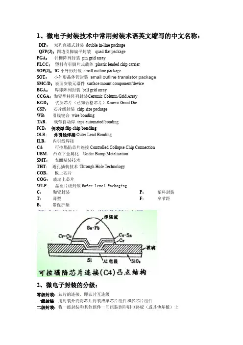
1、微电子封装技术中常用封装术语英文缩写的中文名称:DIP:双列直插式封装double in-line packageQFP(J):四边引脚扁平封装quad flat packagePGA:针栅阵列封装pin grid arrayPLCC:塑料有引脚片式载体plastic leaded chip carrierSOP(J):IC小外形封装small outline packageSOT:小外形晶体管封装small outline transistor packageSMC/D:表面安装元器件surface mount component/deviceBGA:焊球阵列封装ball grid arrayCCGA:陶瓷焊柱阵列封装C eramic Column Grid ArrayKGD:优质芯片(已知合格芯片)Known Good DieCSP:芯片级封装chip size packageWB:引线键合wire bondingTAB:载带自动焊tape automated bondingFCB:倒装焊flip chip bondingOLB:外引线焊接Outer Lead BondingILB:内引线焊接C4:可控塌陷芯片连接Controlled Collapse Chip ConnectionUBM:凸点下金属化Under Bump MetalizationSMT:表面贴装技术THT:通孔插装技术Through Hole TechnologyCOB:板上芯片COG:玻璃上芯片WLP:晶圆片级封装Wafer Level PackagingC:陶瓷封装P:塑料封装T:薄型F:窄节距B:带保护垫2、微电子封装的分级:零级封装:芯片的连接,即芯片互连级一级封装:用封装外壳将芯片封装成单芯片组件和多芯片组件二级封装:将一级封装和其他组件一同组装到印刷电路板(或其他基板)上三级封装:将二级封装插装到母板上3、微电子封装的功能:1)电源分配:保证电源分配恰当,减少不必要的电源消耗,注意接地线分配问题。
![微电子封装技术讲义06.07[1]](https://uimg.taocdn.com/8423da2c5acfa1c7aa00ccc4.webp)
微电子封装技术Chapter 1Introduction第1章简介1.The development characteristics and trends of microelectronics packaging.微电子封装的发展特点和趋势。
2.The func tions of microelectronics packaging. 微电子封装的功能。
3.The levels of microelectronics packaging technology.微电子封装技术水平。
1.4.The methods for chip bonding. 芯片连接的方法Chapter 2Chip interconnection technology第2章芯片互连技术It is one of the key chapters它是一个关键的章节1.The Three kinds of chip interconnection, and their characteristics and applications. 三种芯片互联方法?他们的特点和应用。
2.The types of wire bonding (WB) technology, their characteristics and working principles.WB技术的种类,特点和工作原理。
3.The working principle and main process of the wire ball bonding.焊球连接的原理和主要步骤。
4.The major materials for wire bonding.用于引线键合的主要材料。
5.Tape automated bonding (TAB) technology:载带自动焊(TAB)的技术:1)The characteristic and application of TAB technology.(TAB)的技术的特点和应用。
——电材专业英语课文翻译Semiconductor Materials• 1.1 Energy Bands and Carrier Concentration• 1.1.1 Semiconductor Materials•Solid-state materials can be grouped into three classes—insulators(绝缘体), semiconductors, and conductors. Figure 1-1 shows the electrical conductivities δ(and the corresponding resistivities ρ≡1/δ)associated with(相关)some important materials in each of three classes. Insulators such as fused(熔融)quartz and glass have very low conductivities, in the order of 1E-18 to 1E-8 S/cm;固态材料可分为三种:绝缘体、半导体和导体。
图1-1 给出了在三种材料中一些重要材料相关的电阻值(相应电导率ρ≡1/δ)。
绝缘体如熔融石英和玻璃具有很低电导率,在10-18 到10-8 S/cm;and conductors such as aluminum and silver have high conductivities, typically from 104 to 106 S/cm. Semiconductors have conductivities between those of insulators and those of conductors. The conductivity of a semiconductor is generally sensitive to temperature, illumination(照射), magnetic field, and minute amount of impurity atoms. This sensitivity in conductivity makes the semiconductor one of the most important materials for electronic applications.导体如铝和银有高的电导率,典型值从104到106S/cm;而半导体具有的电导率介乎于两者之间。

Microelectronics packaging technology(R eview contents)Chapter 1:Introduction1.The development characteristics and trends of microelectronics packaging.2.The functions of microelectronics packaging.3.The levels of microelectronics packaging technology.4.The methods for chip bonding.Chapter 2:Chip interconnection technologyIt is one of the key chapters1.The Three kinds of chip interconnection, and their characteristics and applications.2.The types of wire bonding (WB) technology, their characteristics and working principles.3.The working principle and main process of the wire ball bonding.4.The major materials for wire bonding.5.Tape automated bonding (TAB) technology:1)The characteristic and application of TAB technology.2)The key materials and technologies of TAB technology.3)The internal lead and outer lead welding technology of TAB technology.6. Flip Chip Bonding (FCB) Technology1)The characteristic and application of flip chip bonding technology2)UBM and multilayer metallization under chip bump;UBM’s structure and material, and the roles ofeach layer.3)The main fabrication method of chip bumps.4)FCB technology and its reliability.5)C4 soldering technology and its advantages.6)The role of underfill in FCB.7)The interconnection principles for Isotropic and anisotropic conductive adhesive respectively. Chapter 3: Packaging technology of Through-Hole components1.The classification of Through-Hole components.2.Focused on:DIP packaging technology, including its process flow.3.The characteristics of PGA.Chapter 4:Packaging technology of surface mounted device (SMD)1.The advantages and disadvantages of SMD.2.The types of SMD.3.The main SMD packaging technologies, focused on:SOP、PLCC、LCCC、QFP.4.The packaging process flow of QFP.5.The risk of moisture absorption in plastic packages, the mechanism of the cracking caused by moistureabsorption, and solutions to prevent for such failure.Chapter 5:Packaging technology of BGA and CSP1.The characteristics of BGA and CSP.2.The packaging technology for PBGA,and its process flow.3.The characteristics of packaging technology for CSP.4.The reliability problems of BGA and CSP.Chapter 6:Multi-Chip Module(MCM)1.The classification and characteristics of MCM2. The assembly technology of MCM.Chapter 7:Electronic packaging materials and substrate technology1. The classification of the materials for electronic packaging, the main requirements for packagingmaterials.2. The types of metals in electronic packaging, and their main applications.3. The main requirements for polymer materials in electronic packaging.4.Classification of main substrate materials, and the major requirements for substrate materials.Chapter 8:Microelectronics packaging reliability1.The basic concepts of electronic packaging reliability.2.The basic concepts for failure mode and failure mechanism in electronic packaging.3.Main failure (defect) modes (types) of electronic packaging.4.The purpose and procedure of failure analysis (FA) ;Common FA techniques (such as cross section, dyeand pry, SEM, CSAM ...).5 The purpose and key factors (such as stress level, stress type …) to design accelerated reliability test. Chapter 9:Advanced packaging technologies1.The concept of wafer level packaging (WLP) technology.2.The key processes of WL-CSP.3.The concept and types of the 3D packaging technologies.Specified Subject 1:LED packaging technology1. Describe briefly the four ways to achieve LED white light, and how they are packaged?2. Describe briefly the difference and similar aspects (similarity) between LED packaging andmicroelectronics packaging.3. And also describe briefly the development trend for LED package technology and the whole LED industryrespectively.Specified Subject 2:MEMS packaging technology1.The differences between micro-electro-mechanical system (MEMS) packaging technology and theconventional microelectronics packaging technologies.2.The function requirements of MEMS packaging.Extra requirement:The common used terms (Abbreviation) for electronic packaging.。
现代微电子封装技术课程复习内容第一章1、什么是电子封装“集成电路(IC)”是指微小化的或微电子的器件,它将这样的一些元件例如三极管、电阻、介电体、电容等集成为一个电学上的电路,使致具有专门的功能”“封装”是指连接集成电路和其他元件到一个系统级的基板上的桥梁或手段,使之形成电子产品”2、电子封装和IC技术发展的关系封装是芯片和电子系统之间的桥梁,集成电路封装技术的发展既受微电子技术中芯片设计和制造技术的推动,同时,封装技术的发展又有力地支撑和推动了整个微电子技术的发展在过去几十年里,为适应集成电路向小型化、高速化、大功率发展的需要,集成电路封装技术得到了不断的提高和改进。
朝着小尺寸、多I/O、高密度、高可靠性、高散热能力、自动化组装的方向发展3、IC芯片发展的特征每块芯片上的元器件数逐年增加特征尺寸不断减小芯片功耗不断增加门的功耗逐年减少4、电子封装的发展特征从插孔式封装到表面贴装从双列式封装经四面有脚的QFP形式发展到球栅阵列BGA以及多芯片MCM封装封装的密度和I/O大大增加封装的尺寸由大尺寸发展到芯片大小的CSP封装5、微电子封装的作用信号的输入、输出端向外界的过渡手段电源的输入、输出端同外界的过渡手段散热保护器件不受外界环境的影响6、微电子封装的分类一级封装一级封装是指芯片级封装,即将芯片封装以形成器件,所以又称器件封装二级封装二级封装是指将元器件连接在印刷电路板上三级或更高级封装7、一般一级封装的互连方式有那些(a) TAB packaging(b) Wire bonding connection(c) Flip-Chip packaging8、二级封装的互连方式有那些(a) THT组装(b) SMT组装(c) BGA组装(d) CSP 组装9、简述IC芯片的制造过程单晶硅碇的形成(单晶成长)硅片加工过程芯片制造:增层,光刻和刻蚀,掺杂,热处理硅片制备测试/拣选封装第二章1、简述引线键合的工艺过程引线键合技术(WB)是将半导体芯片焊区与微电子封装的I/O引线或基板上的金属布线焊区用金属丝连接起来的工艺技术在较低的温度下,通过施加压力,使金属丝发生塑性变形,来完成固相结合。
《电子封装技术专业学科(专业)概论》课程教学大纲一、课程名称(中英文)中文名称:学科(专业)概论英文名称:An Introduction to Discipline (Specialty)二、课程编码及性质课程编码:0400022课程性质:必修课三、学时与学分总学时:16学分:1四、先修课程军训、入学教育、实验室参观五、授课对象本课程面向刚入校的“电子封装技术专业”学生,也可以供“电子制造科学与工程专业”和“微电子工程专业”入学新生选修。
六、课程教学目的本课程是本专业入学新生快速了解专业领域的历史、现状、发展,培养学生专业兴趣的导入与介绍课程。
主要包括:1.系统介绍从电子管、半导体、集成电路再到信息电子产品的制造发展历程,理解信(信息电子产品)和衣、食、住、行相提并论,成为人们现代人们生活的必须(需),从而深入掌握信息电子产品制造的内涵、外延;2.介绍本专业的教学规划、教学体系、四年的课程安排,各课程的特色与相互关联,培养新生四年大学学习与生活的规划能力;3.重点介绍集成电路制造、电子封装技术、电子组装技术、半导体照明、太阳能光伏、电子显示技术等的基本知识、应用领域、发展方向,理解人类未来电子产品制造的蓝图;4.培养学生从事电子制造领域的素质和能力。
表1 课程目标对毕业要求的支撑关系七、教学重点与难点:教学重点:1)向学生介绍本专业的基本状况与发展前景,激发学生对本专业的兴趣,立志投身中国的电子制造业;2)介绍本专业的教学规划、教学体系、四年的课程安排,介绍各课程的特色与相互关联;3)重点介绍集成电路制造、电子封装技术、电子组装技术、半导体照明、太阳能光伏、电子显示技术等的基本知识、应用领域、发展方向。
教学难点:学科(专业)概论是电子封装技术专业的必修课程,具有入门、宏观、概要等特征,对学生的四年专业学习起着引领、指导、启发等作用,是进入大学学习的最重要认识课程。
由本专业的资深教授讲授,间或聘请专业领域的著名人士以专题讲座形式进行。
微电子封装技术重点
一、引言
微电子封装技术是元器件的重要组成部分,是电子元器件的基本技术,是现代电子产业发展的基础。
电子封装技术在电子产品的制造和使用过程
中扮演着十分重要的角色,是提高电子产品可靠性和性能、降低成本的重
要手段,是极具发展前景的新兴技术。
二、封装技术体系
封装技术是一个复杂的科学体系,它是电子技术与材料学和加工工艺
结合的结果,它集成了电子元器件、电路板、电缆和终端用户的工程技术,满足电子产品性能、可靠性、结构尺寸、布线、容积、成本等要求。
封装技术体系涵盖的技术领域有:
1、元器件封装工艺:包括元器件的制备、设计和加工,以及封装结
构和结构尺寸等;
2、陶瓷封装技术:包括陶瓷封装的制备、设计和加工,以及封装结
构和结构尺寸等;
3、封装材料的开发、研究和应用:包括封装材料的性能选择和使用,电子元器件的封装介质等;
4、封装工艺自动化:包括封装自动化装备,自动检测装置等;
5、封装性能的测试:包括封装介质的性能测试、电气性能测试和可
靠性测试等;
三、封装技术的发展趋势。
第一章绪论一、微电子封装技术的发展特点和趋势发展特点:(1)微电子封装向高密度和高I/O引脚数发展,引脚由四边引出向面阵列发展(2)微电子封装向表面安装式封装(SMP)发展,以适合表面安装技术(SMT)(3)从陶瓷封装向塑料封装发展(4)从注意发展IC芯片向先发展后道封装再发展芯片转移发展趋势:(1)微电子封装具有的I/O引脚数将更多(2)微电子封装应具有更高的电性能和热性能(3)微电子封装将更轻、更薄、更小(4)微电子封装将更便于安装、使用和返修(5)微电子封装的可靠性会更高(6)微电子封装的性能价格比会跟高,而成本却更低,达到物美价廉二、微电子封装技术的分级芯片互连级(零级封装)、一级封装(多芯片组件)、二级封装(PWB或卡)三级封装(母板)三、芯片粘接方式有哪几种(1)Au—Si合金共熔法(2)Pb—Sn合金片焊接法(3)导电胶粘接法(4)有机树脂基粘接法四、微电子封装的功能1、电源分配2、信号分配3、散热通道4、机械支撑5、环境保护第二章芯片互连技术一、引线键合的分类及特点1、热压焊压悍时芯片与焊头均要加热,容易使焊区和焊丝形成氧化层。
同时,由于芯片加热温度高,压焊时间一长,容易损害芯片,也容易在高温下形成异质金属影响器件的可靠性和寿命2、超声焊焊接强度高于热压焊,不需加热可在常温下进行,因此对芯片性能无损害,可根据不同的需要随时调节超声键合能量,改变键合条件3、金丝球焊操作方便灵活,而且焊点牢固,压点面积大,又无方向性,故可实现微机控制下的高速自动化焊接二、金丝球焊的主要原理三、引线键合的主要材料热压焊、金丝球焊主要选用Au丝,超声焊主要用Al丝和Si—Al丝,还有少量的Cu—Al和Cu—Si—Al等四、载带自动焊(TAB)技术的特点及应用特点:(1)TAB结构轻、薄、短、小(2)TAB的电极尺寸、电极与焊区节距均比WB大为减小(3)相应可容纳更高的I/O引脚数(4)TAB的引线电阻、电容和电感均比WB的小得多(5)采用TAB互连,可对各类IC芯片进行筛选和测试,确保器件是优质芯片(6)TAB采用Cu箔引线,导热和导电性能好,机械强度高(7)TAB的键合拉力比WB高,可提高芯片可靠性(8)TAB使用标准化的卷轴长带,对芯片实行自动化多点一次焊接,同时安装和外引线焊接可实现自动化,从而提高电子产品的生产效率,降低生产成本应用:TAB技术已不单能满足高I/O数的各类IC芯片的互连需求,而且以作为聚酰亚胺(PI)—粘接剂—Cu箔三层软引线载带的柔性引线,成为广泛应用于电子整机内部和系统互连的最佳方式。
Microelectronics packaging technology
(R eview contents)
Chapter 1:Introduction
1.The development characteristics and trends of microelectronics packaging.
2.The functions of microelectronics packaging.
3.The levels of microelectronics packaging technology.
4.The methods for chip bonding.
Chapter 2:Chip interconnection technology
It is one of the key chapters
1.The Three kinds of chip interconnection, and their characteristics and applications.
2.The types of wire bonding (WB) technology, their characteristics and working principles.
3.The working principle and main process of the wire ball bonding.
4.The major materials for wire bonding.
5.Tape automated bonding (TAB) technology:
1)The characteristic and application of TAB technology.
2)The key materials and technologies of TAB technology.
3)The internal lead and outer lead welding technology of TAB technology.
6. Flip Chip Bonding (FCB) Technology
1)The characteristic and application of flip chip bonding technology
2)UBM and multilayer metallization under chip bump;UBM’s structure and material, and the roles of
each layer.
3)The main fabrication method of chip bumps.
4)FCB technology and its reliability.
5)C4 soldering technology and its advantages.
6)The role of underfill in FCB.
7)The interconnection principles for Isotropic and anisotropic conductive adhesive respectively. Chapter 3: Packaging technology of Through-Hole components
1.The classification of Through-Hole components.
2.Focused on:DIP packaging technology, including its process flow.
3.The characteristics of PGA.
Chapter 4:Packaging technology of surface mounted device (SMD)
1.The advantages and disadvantages of SMD.
2.The types of SMD.
3.The main SMD packaging technologies, focused on:SOP、PLCC、LCCC、QFP.
4.The packaging process flow of QFP.
5.The risk of moisture absorption in plastic packages, the mechanism of the cracking caused by moisture
absorption, and solutions to prevent for such failure.
Chapter 5:Packaging technology of BGA and CSP
1.The characteristics of BGA and CSP.
2.The packaging technology for PBGA,and its process flow.
3.The characteristics of packaging technology for CSP.
4.The reliability problems of BGA and CSP.
Chapter 6:Multi-Chip Module(MCM)
1.The classification and characteristics of MCM
2. The assembly technology of MCM.
Chapter 7:Electronic packaging materials and substrate technology
1. The classification of the materials for electronic packaging, the main requirements for packaging
materials.
2. The types of metals in electronic packaging, and their main applications.
3. The main requirements for polymer materials in electronic packaging.
4.Classification of main substrate materials, and the major requirements for substrate materials.
Chapter 8:Microelectronics packaging reliability
1.The basic concepts of electronic packaging reliability.
2.The basic concepts for failure mode and failure mechanism in electronic packaging.
3.Main failure (defect) modes (types) of electronic packaging.
4.The purpose and procedure of failure analysis (FA) ;Common FA techniques (such as cross section, dye
and pry, SEM, CSAM ...).
5 The purpose and key factors (such as stress level, stress type …) to design accelerated reliability test. Chapter 9:Advanced packaging technologies
1.The concept of wafer level packaging (WLP) technology.
2.The key processes of WL-CSP.
3.The concept and types of the 3D packaging technologies.
Specified Subject 1:LED packaging technology
1. Describe briefly the four ways to achieve LED white light, and how they are packaged?
2. Describe briefly the difference and similar aspects (similarity) between LED packaging and
microelectronics packaging.
3. And also describe briefly the development trend for LED package technology and the whole LED industry
respectively.
Specified Subject 2:MEMS packaging technology
1.The differences between micro-electro-mechanical system (MEMS) packaging technology and the
conventional microelectronics packaging technologies.
2.The function requirements of MEMS packaging.
Extra requirement:
The common used terms (Abbreviation) for electronic packaging.。