官方例程Kinetis100MHz ADC
- 格式:pdf
- 大小:1.61 MB
- 文档页数:9
飞思卡尔ADC例程指南例程功能飞思卡尔Kinetis E系列KE02产品ADC_demo例程实现ADC的FIFO操作,不断采样温度、BandGap及VREFH,且在三者采样完成后触发中断,串口打印出采样结果。
相关代码参考KE02-SC.zip中的ADC_demo例程。
运行平台✓FRDM-KE02Z✓IAR ARM IDE运行例程(IAR)1)使用USB cable连接FRDM-KE02Z开发板Min-B USB连接器(J6);2)加载ADC_demo工程后,选择【FLASH_128KB】,点击进行编译;3)编译成功后,点击进入调试界面;4)进入调试界面后,点击运行例程。
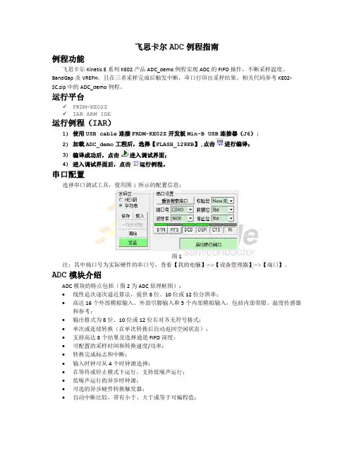
串口配置选择串口调试工具,使用图1所示的配置信息;图 1注:其中端口号为实际硬件的串口号,查看【我的电脑】->【设备管理器】->【端口】。
ADC模块介绍ADC模块的特点包括(图2为ADC原理框图):∙线性追次逐次逼近算法,提供8位、10位或12位分辨率;∙高达16个外部模拟输入、外部引脚输入和5个内部模拟输入,包括内部带隙、温度传感器和参考;∙输出格式为8位、10位或12位右对齐无符号格式;∙单次或连续转换(在单次转换后自动返回空闲状态);∙支持高达8个结果及选择通道FIFO深度;∙可配置的采样时间和转换速度/功率;∙转换完成标志和中断;∙输入时钟可从4个时钟源选择;∙在等待或停止模式下运行,支持低噪声运行;∙低噪声运行的异步时钟源;∙可选的异步硬件转换触发器;∙自动中断比较,带有小于、大于或等于可编程值;图2 ADC模块原理框图代码说明引脚名称方向功能PTH2 输出控制绿色led灯ADC_FIFO_Init(ADC_BASE_PTR)ADC_Isr()主程序流程图运行结果代码烧录完成后,主程序运行到等待字符输入状态(如图3和图4所示)。
图3N返回图4输入任意字符,ADC FIFO操作再次运行且绿灯翻转,并回到等待字符输入状态(如图5和图6所示)图 5图 6参考手册KE02芯片参考手册 MKE02Z64M20SF0RM/files/32bit/doc/ref_manual/MKE02Z64M20SF0RM.pdf?fpsp=1KE02芯片数据手册 MKE02P64M20SF0/files/32bit/doc/data_sheet/MKE02P64M20SF0.pdf?fpsp=1FRDM-KE02Z板原理图/files/soft_dev_tools/hardware_tools/schematics/FRDM-KE02Z_SCH.pdf?fpsp=1&WT_TYPE=Schematics&WT_VENDOR=FREESCALE&WT_FILE_FORMAT=pdf&WT_ ASSET=Downloads&sr=1FRDM-KE02Z用户指南/files/microcontrollers/doc/user_guide/FRDM-KE02ZUM.pdf?fpsp=1KE02-SC例程包/zh-Hans/webapp/sps/site/prod_summary.jsp?code=FRDM-KE02Z&fpsp=1&tab=Design_Tools_Tab。
作者:潘峰北京联合大学实训基地微博:/u/1262858854QQ:66797490博客:/panpan_0315/blog/本章内容仅供个人学习之用,请勿用于其它用途。
1.2DAC数模转换模块1.7.1 DAC简介Kinetis10包含两个独立的12位数模转换模块,DAC0和DAC1,用于将数字转换成对应的模拟电压。
转换后的模拟电压可由外部引脚输出,也可以通过芯片内部连接输入到比较器模块、放大器模块、和模数转换模块。
DAC的参考电压可以二选一,一个来自外部或VREF模块的输出,默认连接到DACREF_1;另一个时VDDA,默认连接到DACREF_2。
如果选择VDDA,则DAC的参考电压为3.3V。
12位二进制的表示范围为0~4095的无符号数。
对应数据转换成模拟电压输出范围从VREF/4096~VREF。
以VREF为3.3V计算,则是约0.8mV~3.3V,数据每变化1,输出电压变化约0.8mV。
将数据放入DAC的数据寄存器(DACx_DATL中的DACDATA[11:0]位),即可将数据转换为模拟电压。
电压Vout= VREF * (1 + DACDAT0[11:0])/4096。
在大量数据转换的应用中,也可以将数据放入DAC的缓冲区,由触发源输入触发信号,在触发信号的触发下,自动挨个将缓冲区中的数据转换为模拟电压。
缓冲区大小为1~16可设置大小的以word为单位的区域,转换的时候,由读指针指向正在转换的数据,可通过访问读指针获知当前正在转换的缓冲区单元。
数据转换的次序为从顶部到底部依次转换,从顶部到底部之间,用户可设置位置标记(watermark)作为预警位置,当读指针指向缓冲区顶部、底部或位置标记处时,都有状态位可供查询,也可以发出中断请求。
触发信号可来自PDB模块的TRIG输出详细可查看PDB模块设置。
同时DAC模块也支持DMA操作,可通过DMA的方式向缓冲区中传递数据,大大提高了效率。
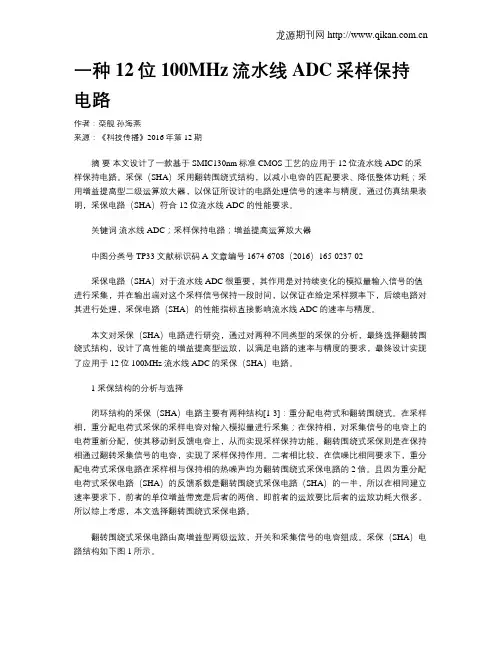
一种12位100MHz流水线ADC采样保持电路作者:栾舰孙海燕来源:《科技传播》2016年第12期摘要本文设计了一款基于SMIC130nm标准CMOS工艺的应用于12位流水线ADC的采样保持电路。
采保(SHA)采用翻转围绕式结构,以减小电容的匹配要求、降低整体功耗;采用增益提高型二级运算放大器,以保证所设计的电路处理信号的速率与精度。
通过仿真结果表明,采保电路(SHA)符合12位流水线ADC的性能要求。
关键词流水线ADC;采样保持电路;增益提高运算放大器中图分类号 TP33 文献标识码 A 文章编号 1674-6708(2016)165-0237-02采保电路(SHA)对于流水线ADC很重要,其作用是对持续变化的模拟量输入信号的值进行采集,并在输出端对这个采样信号保持一段时间,以保证在给定采样频率下,后续电路对其进行处理,采保电路(SHA)的性能指标直接影响流水线ADC的速率与精度。
本文对采保(SHA)电路进行研究,通过对两种不同类型的采保的分析,最终选择翻转围绕式结构,设计了高性能的增益提高型运放,以满足电路的速率与精度的要求,最终设计实现了应用于12位100MHz流水线ADC的采保(SHA)电路。
1 采保结构的分析与选择闭环结构的采保(SHA)电路主要有两种结构[1-3]:重分配电荷式和翻转围绕式。
在采样相,重分配电荷式采保的采样电容对输入模拟量进行采集;在保持相,对采集信号的电容上的电荷重新分配,使其移动到反馈电容上,从而实现采样保持功能。
翻转围绕式采保则是在保持相通过翻转采集信号的电容,实现了采样保持作用。
二者相比较,在信噪比相同要求下,重分配电荷式采保电路在采样相与保持相的热噪声均为翻转围绕式采保电路的2倍。
且因为重分配电荷式采保电路(SHA)的反馈系数是翻转围绕式采保电路(SHA)的一半,所以在相同建立速率要求下,前者的单位增益带宽是后者的两倍,即前者的运放要比后者的运放功耗大很多。
飞思卡尔Kinetis微控制器支持开发更便携更智能的血糖仪挑战打破传统方法枯燥、依从性差的弊端,以便携、寿命长为特性,设计一款基于移动互联网技术具有血糖采集和综合维护功能的糖尿病管理系统。
解决方案飞思卡尔Kinetis L系列微控制器,采用ARMCortex-MO+内核,具有超低功耗特性,配备了丰富的模拟、通讯和控制外设。
糖护士采用了飞思卡尔Kinetis KL05 MCU 实现了性能和功耗的完美平衡。
应用工程师不再因为受制于功耗的问题而局限于8位或者是16位MCU。
KL05具有优化的动态和停止电流并提供出色的处理性能,同时还提供多种片上闪存密度以及丰富的模拟模块、连接功能和HMI外设供工程师选择。
优势产品形态方面,传统的血糖仪是独立的设备,需要配备屏幕和大容量的电池,因此设备体积较大,不具备便携性。
糖护士采用了Kinetis KL05MCU,做成手机配件的形式,通过耳机接口与手机搭配使用,无需单独配备屏幕,因此,整体功耗、体积和重量都大大降低。
经测试,50mAh的纽扣电池可以支持5年或4000次的血糖检测使用,而整机(含电池)重量仅有9克。
该产品通过国家食品药品监督局严格认证,获得CFDA(国家食品药品监督管理总局)证书(湘食药监械(准)字2014第2400052号)。
在数据的管理方面,使用传统血糖仪的患者需要把测量的血糖数据抄到本子上,就诊时拿给医生看,这样麻烦且血糖数据的变化趋势展示不直观。
有了糖护士,糖尿病患者测量的数据自动存储到智能手机和云端,它可以很方便地以曲线、表格的形式展示数据。
通过移动互联网,医生可以远程查看数据,然后指导患者调整饮食、运动、用药。
通过糖护士软件,患者还可以方便的记录日常饮食、运动、用药情况,通过设置提醒确保按时测量血糖和用药,并且可以在软件上浏览丰富的糖尿病知识。
寻找合适的技术合作伙伴北京糖护科技有限公司首席技术官(CTO)Brent Zheng (郑志华)表示:“我们需要寻找既能高速运算又具有低功耗特性的MCU,普通的8/16位MCU已经无法满足糖护士产品研发的需求,一筹莫展之时,我们找到了飞思卡尔的KL05,它完全能满足我们对功耗和运算速度的双向需求。
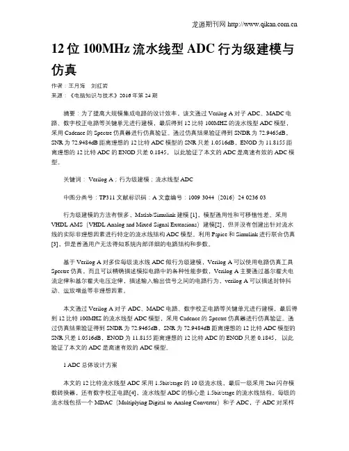
12位100MHz流水线型ADC行为级建模与仿真作者:王月海刘红岩来源:《电脑知识与技术》2016年第24期摘要:为了提高大规模集成电路的设计效率,该文通过Verilog-A对子ADC、MADC电路、数字校正电路等关键单元进行建模,最后得到12比特100MHZ的流水线型ADC模型,采用Cadence的Spectre仿真器进行仿真验证。
通过仿真结果验证得到SNDR为72.9465dB,SNR为72.9484dB距离理想的12比特ADC模型的SNR只差1.0516dB,ENOD为11.8155距离理想的12比特ADC的ENOD只差0.1845,以此验证了本文的ADC是高速有效的ADC模型。
关键词: Verilog-A;行为级建模;流水线型ADC中图分类号:TP311 文献标识码:A 文章编号:1009-3044(2016)24-0236-03行为级建模的方法有很多,Matlab/Simulink建模 [1],模型通用性和可移植性差。
采用VHDL-AMS(VHDL Analog and Mixed-Signal Extensions)建模[2],但并没有创建出针对流水线的实际非理想因素进行特定的流水线结构ADC模型。
利用Pspice和Simulink进行联合仿真[3],但是普通用户无法得知系统内部详细的电路结构和参数。
基于Verilog-A对多位每级流水线ADC做行为级建模,Verilog-A可以使用电路仿真工具Spectre仿真,而且可以精确描述模拟电路中的各种性能参数,Verilog-A主要通过基尔霍夫电流定律和基尔霍夫电压定律,描述输入输出信号之间的电路行为,verilog-A可以描述时钟抖动、运放增益等非理想因素。
本文通过Verilog-A对子ADC、MADC电路、数字校正电路等关键单元进行建模,最后得到12比特100MHZ的流水线型ADC模型,采用Cadence的Spectre仿真器进行仿真验证。
【原创】从零入手Kinetis系统开发(七)之ADC模块•2012-02-2922:52发表系统分类:嵌入式系统自定义分类:Kinetis•标签:Kinetis K60IAR ADC今天是2月最后一天,而且还是四年一次的2月29日,为了纪念这难得的一天还是决定写点东西,呵呵。
在连续写了几篇有关飞思卡尔开发环境(IDE)的博客之后,觉着虽然有点新意有点小技巧在里面,不过看多了估计大家也看腻歪了也会觉着其实写了那么多没实际内容(其实真有的,这些小技巧我还是花费了一些心思专研了一番的,哈哈),所以这次就再爆点实料,继续更新从零入手系列。
前一阵儿,自己的确在找状态,因为放假回来之后觉着对Kinetis生疏了不少,思路有些空白,所以私底下弥补了一番,真的是台上十分钟,台下十年功,当然不是在给开源者邀功颂德之类的,就是明白了为什么好多人不愿意开源,其实一方面可能的确涉及到自己的知识产权和核心的东西,还有就是想要开源不单单是简单的贴出源代码这么简单(这点很同意AET博主说的,其实作为开源者也是),作为开源者,开源常常会拖带一些麻烦的义务还有因为自己辛苦的劳动被别人简单的贴出去连转载两个字都不加的委屈,说真的,简单的贴出源代码,估计没几个人能看懂,当然代码风格好的就不算了,嘿嘿,所以开源需要很大的勇气。
晕,又扯偏了,呵呵,还是继续说正事吧,哈哈~又是老惯例,啰嗦了一堆,所以老朋友可以直接跳的该段了,哈哈,本篇就拿Kinetis的ADC模块开刀,其实有过网友说急需DMA的例程还有说写写细说寄存器使用方法之类的,不是不想写,是的确我还没用到DMA之类的,所以可能还需一些时日,不过保证肯定会有的,如果有先写出来的还是欢迎分享出来,独乐乐不如众乐乐嘛,哈哈,下面进入正题:1.Kinetis的ADC模块的一些特点(以K60为例),挑重要的说了,一些AD模块常见的特点就不提了,呵呵:(1)最高16位AD转换精度,逐次逼近型的,所以速度没问题,而且能做到如此精度已实属不易了,再往高估计就该换Σ-Δ的了;(2)最多4对差分模拟输入通道和24个单端模拟输入通道,对一般工业应用足够了,其实在对AD要求不高的应用还是用内部AD好些,选外部AD的话一是操作起来麻烦,还有就是对模拟电路布局布线上还是有些技巧的;(3)输出精度可选,例如差分的话可编程16位,13位,11位和9位模式,单端的话可编程为16位,12位,10位和8位,不明白为什么差分精度非要比单端多1位,有知道的希望不吝告诉一下,在下面留言即可,呵呵;(4)输入时钟可选四种时钟,即bus_clock,bus_clock/2,ALTCK,ADACK;(5)内设内部温度传感器,用于监控芯片温度,这个还是有一定用途的,不过对他的精度不要有过高期望;(6)硬件平均功能,对AD转换结果在队列里平均之后输出,挺实用的,要是再能对列排列一下就好了,咳咳,有点要求太高了,哈哈;(7)带自校准模式,用过外部AD的知道,这个功能是必须的但又颇有点小道道的,深入做过项目的肯定知道,呵呵;(8)最高64倍PGA(programable gain Amplifier),加上这个还是让俺们给飞思卡尔加点满意分的,哈哈。
Freescale Semiconductor, Inc. 文档编号:AN4911应用笔记修订版0,2014年4月利用MKV31F实现三相PMSM无传感器磁场定向控制 (FOC)作者:Matus Plachy1 简介本应用笔记是DRM148(无传感器PMSM磁场定向控制)的补充,描述了该应用所用的MCU外设、硬件设置和测量结果。
目录1简介 (1)2MCU外设 (2)2.1用于产生6通道PWM的FlexTimer0配置 (2)2.2ADC和PDB模块配置 (4)2.3ADC转换时序、电流和电压采样 (4)2.4电流测量 (5)2.5SPI配置 (8)2.6SCI (UART) 配置 (8)3中断 (8)3.1ADC1中断 (8)3.2I/O端口中断 (9)3.3PDB错误中断 (9)4项目文件结构 (10)5存储器使用情形 (12)6硬件设置 (12)6.1硬件设置和跳线配置 (12)7测量结果 (16)7.1CPU负荷和执行时间 (16)7.2FreeMASTER结果 (17)8结论 (17)9参考文献 (18)10缩略语 (18)11修订历史 (18)2 MCU外设表1总结了Kinetis KV31F MCU上的外设及其在PMSM无传感器矢量控制应用中的使用情况:表1. Kinetis KV31F外设概览Kinetis KV31F外设应用中使用用途组别模块模块或通道数模拟ADC025个单端通道,其中可构成4个差分对3通道直流母线电压和电机相电流检测ADC125个单端通道,其中可构成4个差分对2通道比较器2个模块,各7通道––DAC1个模块––通信SPI2个模块,SPI0有6个片选信号,SPI1有4个片选信号1个模块MOSFET驱动器配置UART3个模块1个模块FreeMASTER通信LPUART1个模块––I2C2个模块––定时器FlexTimer8通道6通道产生6通道PWM用于电机控制2通道––2通道––8通道––PDB2通道用于ADC触发2通道用于触发直流母线电压和相电流采样2通道用于DAC触发––PIT4通道––LPT1个模块––其他eDMA16通道––2.1 用于产生6通道PWM的FlexTimer0配置FlexTimer模块(FTM) 是一个包含2至8通道的定时器,支持输入捕捉、输出比较以及产生PWM信号功能以实现来控制电机和电源管理应用。
Freescale Semiconductor Application Note1IntroductionThe Programmable Delay Block (PDB) provides controllable delays from either an internal or an external trigger, or a programmable interval tick to the hardware trigger inputs of the ADCs. This functionality is required for applications when precise timing of ADC conversions are required, or when the measured signal must be filtered using precise sampling.The PDB is necessary in some motor control specific applications which require advanced ADC to PWM synchronization. This application note describes the set-up of the PDB, routing of the signal onto a GPIO pin, and sequence error handling. A typical application is the BLDC six-step method. This application note focuses on the Kinetis K60 family, the FlexTimer, and 16-bit ADCs.2Understanding PDBterminologyThis section describes the important terms used in the Kinetis K60 reference manual that relate to this application.Document Number:AN4822Rev. 0, 12/2013Contents1.Introduction . . . . . . . . . . . . . . . . . . . . . . . . . . . . . . . . . 12.Understanding PDB terminology . . . . . . . . . . . . . . . . 13.PDB Set-up . . . . . . . . . . . . . . . . . . . . . . . . . . . . . . . . . 24.Routing the PDB pre-trigger onto a GPIO pin . . . . . . 45.PDB sequence error handling . . . . . . . . . . . . . . . . . . . 46.Application example . . . . . . . . . . . . . . . . . . . . . . . . . . 57.Reference documentation . . . . . . . . . . . . . . . . . . . . . . 68.Revision history . . . . . . . . . . . . . . . . . . . . . . . . . . . . . 7Tips and Tricks Using PDB in Motor Control Applications on Kinetisby Ivan LovasFreescale Semiconductor, Inc.PDB Set-upFigure 1 illustrates the arrangement of the FlexTimer to the ADCs in association to the terms used.Figure 1. Internal arrangement of PDBInput trigger source —One possible input source which starts the PDB counter for all PDB channels. All possible input sources can be found in the chip reference manual, in the section “PDB Input Trigger Connections.” The input trigger source number must be entered into register PDBx_SC, field TRGSEL.PDB channel —Each PDB channel is associated with one ADC. This means that ADC0 is associated with PDB channel 0 and ADC1 is associated with PDB channel 1.Pre-trigger delay —Each pre-trigger is generated after a predefined delay, which is measured from the input trigger event. After this delay, an ADC convertor begins to measure and the result of conversion is stored in the result register corresponding to the respective pre-trigger delay. Relationships between pre-triggers and result registers are described in the Table 1.3PDB Set-upTo accurately synchronize between the FlexTimer and ADC, three peripherals must be configured. Only the settings necessary for synchronization will be described. The settings for PWM generation and ADC module are application specific and therefore cannot be described in detail here.Table 1. Relation between pre-triggers and result registersRespective Pre-Trigger DelayRegister with Conversion Result PDB0_CH0_DL Y0ADC0_RA PDB0_CH0_DL Y1ADC0_RB PDB0_CH1_DL Y0ADC1_RA PDB0_CH1_DL Y1ADC1_RBPDB Set-upExample1. PDB settingsPDBinit(void){SIM_SCGC6 |= SIM_SCGC6_PDB_MASK; // enable clock for PDB modulePDB0_MOD = MODULO;// modulo for PDB counter should be same as FTM modulo//enable required pre-triggers, enable back-to-back operationPDB0_CH1C1 = PDB_C1_EN (0x03) | PDB_C1_TOS(0x03) | PDB_C1_BB (0x02);PDB0_CH0C1 = PDB_C1_EN (0x03) | PDB_C1_TOS(0x03) | PDB_C1_BB (0x02);PDB0_CH0DLY0 = 150;// delay for first pre-trigger of PDB channel 0PDB0_CH1DLY0 = 200; // delay for first pre-trigger of PDB channel 1PDB0_SC = PDB_SC_PDBEN_MASK| PDB_SC_PRESCALER(0x0)| PDB_SC_TRGSEL(0x8) // 0x8=FTM0| PDB_SC_MULT(0)| PDB_SC_LDOK_MASK| PDB_SC_PDBEIE_MASK;}FlexTimer init trigger signal needs to be routed out of the FlexTimer by the FlexTimer settings command.Example2. FlexTimer settingsFTM0_EXTTRIG |= FTM_EXTTRIG_INITTRIGEN_MASK;Example3. ADC settingsADC1_SC2 |= ADC_SC2_ADTRG_MASK; // Enable H/W trigger for ADC1ADC0_SC2 |= ADC_SC2_ADTRG_MASK; // Enable H/W trigger for ADC0SIM_SOPT7 = 0; // Select H/W trigger source for the ADCsADC1_SC1A = ADC_SC1_ADCH(11); // BEMF voltage measurement (ADC1_RA)ADC1_SC1B = ADC_SC1_AIEN_MASK | ADC_SC1_ADCH(12);// DC-Bus current (ADC1_RB)ADC0_SC1A = ADC_SC1_ADCH(19); // DC voltage (ADC0_RA)ADC0_SC1B = ADC_SC1_AIEN_MASK | ADC_SC1_ADCH(14); // Pressure sensor (ADC0_RB)Routing the PDB pre-trigger onto a GPIO pin4Routing the PDB pre-trigger onto a GPIO pinTo check whether the synchronization is working correctly, it is good to route the pre-trigger signal to a GPIO pin. For this purpose, you can use an unused channel of the FlexTimer.The following settings are necessary to prepare the trigger diagnostic pin. This example selects the FlexTimer channel 7, however it is possible to select any free FlexTimer channel.FTM0_C7SC |= FTM_CnSC_MSA_MASK;// Set the output compare mode to FTM channel 7FTM0_C7SC |= FTM_CnSC_ELSA_MASK;// Enable the output toggle on matchPORTD_PCR7 |= PORT_PCR_MUX(4);// Set the pin alternative for PORTD 7 - Route the FTM signal to a pinNext, fill the FlexTimer value register with the value of the required delay. If the PDB delay is changing periodically, the FlexTimer value register requires periodic updates.FTM0_C7V = PDB0_CH1DLY0; // Enter the value of the delay from the pre-trigger delay register5PDB sequence error handlingThe ADC n block can be triggered for a conversion by one pre-trigger from PDB channel n. When one conversion is in progress that is triggered by one of the pre-triggers from PDB channel n, then a new trigger from the PDB channel's corresponding pre-trigger m cannot be accepted by ADC n, and ERR[m] is set. For example, in the Sensorless BLDC six-step control, ADC channels are periodically switched according to rotor position. This principle may cause a PDB sequence error. To avoid this type of error, it is necessary to switch to the channel only when no conversion is active. It is recommended to only allow switching after the ADC conversion complete interrupt is received.Changing the ADC channel can be also tricky, because writing SC1A while SC1A is actively controlling a conversion, aborts the current conversion therefore; the conversion complete interrupt is not called, the result register is not read, the PDB flag is not cleared, and a PDB sequence error occurs. In Software Trigger mode, when SC2[ADTRG]=0, writes to SC1A it subsequently initiates a new conversion ifSC1[ADCH] contains a value other than all 1s.When the PDB is not managed correctly, PDB sequence errors can occur. These situations occur given several scenarios. For example:•When delay0 and delay1 of one PDB channel are too close and the first conversion is not complete before the start of a new conversion.•When the asynchronous event that causes the conversion complete flag is not cleared on time anda new conversion is requested, such as:—an interrupt with a high priority causes the COCO flag not to be cleared on time.—using break points during application debugging.•When the ADC channel is changed during an active ADC conversion, such as:—a BLDC motor with Hall sensors controlled by interrupts.—a slow control loop is asynchronous to a fast control loop.Application example After a PDB sequence error occurs the PDB remains inactive until the errors are cleared. Before a PDB error is cleared, the PDB module must be disabled and re-enabled after errors are cleared.Example4. An example of a PDB sequence error interrupt routinevoid PDB_error_isr(void){PDB0_SC &= ~PDB_SC_PDBEN_MASK; // disable PDBPDB0_CH0S &= ~PDB_S_ERR_MASK; // reset error CH0PDB0_CH1S &= ~PDB_S_ERR_MASK; // reset error CH1PDB0_SC |= PDB_SC_PDBEN_MASK; // Enable PDB}This function is called when a PDB error occurs. Bit PDBx_SC_PDBEIE must be set to enable the sequence error interrupt. It is not required to set bit PDBx_SC_PDBIE to enable the error interrupt.6Application exampleFigure2 illustrates a practical usage of PDB synchronization when a noisy signal is measured. As shown, the measured signal (orange signal) is effectively filtered by proper sampling. Samples are taken after a transient event finishes, so only clean signal is measured. Points where the samples are taken are indicated by the blue diagnostic signal.Reference documentation Figure 2. Example of proper setting of PDB trigger, for noisy signal filtering7Reference documentationK60 Sub-Family Reference Manual for 100 MHz devices in 100 pin packages (document K60P100M100SF2V2RM)K60 Sub-Family Reference Manual for 100 MHz devices in 121 pin packages (document K60P121M100SF2V2RM)K60 Sub-Family Reference Manual for 100 MHz devices in 144 pin packages (document K60P144M100SF2V2RM)K60 Reference Manual (document number K60P120M100SF2RM)K60 Sub-Family Reference Manual for 100 MHz devices in 100 pin packages (document K60P100M100SF2RM)Legend:Orange waveform: Noisy signal to be measured.Blue waveform: Diagnostic signal (toggled on the ADC trigger).Revision history K60 Sub-Family Reference Manual for 100 MHz devices in 121 pin packages(document K60P121M100SF2RM)K60 Sub-Family Reference Manual for 100 MHz devices in 144 pin packages(document K60P144M100SF2RM)8Revision historyRevision 0 is the initial release of the document.Document Number:AN4822 Rev. 012/2013Information in this document is provided solely to enable system and software implementers to use Freescale products. There are no express or implied copyright licenses granted hereunder to design or fabricate any integrated circuits based on the information in this document.Freescale reserves the right to make changes without further notice to any products herein. Freescale makes no warranty, representation, or guarantee regarding the suitability of its products for any particular purpose, nor does Freescale assume any liability arising out of the application or use of any product or circuit, and specifically disclaims any and all liability, including without limitation consequential or incidental damages. “Typical” parameters that may be provided in Freescale data sheets and/or specifications can and do vary in different applications, and actual performance may vary over time. All operating parameters, including “typicals,” must be validated for each customer application by customer’s technical experts. Freescale does not convey any license under its patent rights nor the rights of others. Freescale sells products pursuant to standard terms and conditions of sale, which can be found at the following address: /SalesTermsandConditions.How to Reach Us:Home Page:Web Support:/supportFreescale, the Freescale logo, and Kinetis are trademarks of Freescale Semiconductor,Inc., Reg. U.S. Pat. & Tm. Off. All other product or service names are the property oftheir respective owners. ARM and the ARM Power logo are the registered trademarksof ARM Limited.© 2013 Freescale Semiconductor, Inc.。
1IntroductionAn analog-to-digital converter (ADC) cannot ensure idealaccuracy by itself. A number of parameters can affect theachievable accuracy of an ADC in an application.For example:•ADC timing (that is, acquisition time, conversion time,sampling time, sampling jitter, and so on)•Power supply characteristics (noise and internalimpedance)•Isolation between digital and analog portions of the dataacquisition system•Internal and external impedance matching•Input/output switching•PCB layoutTo achieve optimal performance, it is necessary to considerthe application note provides comprehensive guidelines on theprocedure. This document gives comprehensive guidelines onhow to correctly select and design the required external RCcomponents for a SAR ADC input based upon a selectedacquisition time and other converter parameters that can befound in the controller documentation.This application note is developed to address a number ofsimilar requests from several customers. One customerreported having performed an investigation of the influence ofthe ADC during sampling, and also the influence of differentvalues of external RC components on performance. TheyApplication Note Rev 1, 04/2014Cookbook for SAR ADC Measurements ADC measurements done properlyby:Rastislav Pavlanin © 2014 Freescale Semiconductor, Inc.Contents1Introduction................................................................12Theoretical background............................................23Example.....................................................................73.1Example 1 - DSC MC86F8257 with 12-bit cyclic ADC..........................................73.2Example 2 - Kinetis K K70FN1M with 16-bit SAR ADC....................................94Conclusion...............................................................125References...............................................................126Revision history (12)observed serious voltage disturbances (voltage drops/peaks) at the ADC input (see Figure 1). This disturbance was even worse in the case of sequential sampling, when the previously measured signal was grounded. The disturbance at the ADC input in this case results from the basic principle of operation of the sample and hold (S/H) circuit inherent in a SAR ADC.These disturbances do not have to introduce a loss of conversion accuracy as long as the ADC timing is set correctly. If appropriate precautions are not taken, a significant reduction in the accuracy of the digital result can occur during the conversion. This application note clearly shows how to avoid this situation by choosing the correct conversion time and external RC components. The examples of correct external RC component design are presented at the end of the application note. The examples clearly demonstrate proper selection of external components for the cyclic and SAR ADC used inFreescale devices and also mention common mistakes related to incorrect selection of external resistance.Figure 1. Voltage drops at ADC input during sampling process2Theoretical backgroundTo achieve the best performance from an ADC, the overall system must be designed and configured correctly.The hardware setup must carefully follow data sheet recommendations, for example:•Place 0.1 µF capacitor positioned as near as possible to the package power pins (one capacitor for each power pins pairs)•Place approximately 100 µF capacitor to power pins•PCB trace lengths should be minimal•It is necessary to consider all parasitic passive components due to PCB traces in your application•Special care must be taken to minimize noise levels on the analog power and reference pins•Use separate power and ground planes for digital and analog supply pins•If the analog and digital circuits are connected to the same power supply a small inductor (or ferrite) should beconnected between digital and analog pins•Separate analog components from noisy digital components by ground planes (not in parallel), and place the analog ground trace around the analog signal traceIn addition the aforementioned recommendations, special attention must be paid to the design and selection of the external RC components. Minimum values for the external RC components must be considered in final calculations. See MC56F825x/MC56F824x Digital Signal Controller (document MC56F825X)In the text below, the basic principle of the sample and hold circuit (S/H) that is inherently part of an ADC is described in detail. An equivalent sampling circuit considered to present the required background theory is shown in Figure 2. To simplify the sampling process all parasitic components are neglected.NOTEIt is desirable to mention that the equivalent sampling circuit in Figure 2 representssimplified form of ADC used in Freescale devices. The equivalent sampling resistanceR SH is represented by total serial resistance connected between sampling capacitance andanalog input pin (sampling switch, multiplexor switches etc.). The sampling capacitanceC SH is represented by total parallel capacitance. For example in a case of Freescale SARADC equivalent sampling capacitance contains bank of capacitances. Each capacitance inthe bank should be charged by the measured input pin voltage during sampling time (lateras acquisition time). During the rest hold and successive approximation time (conversionsteps) the energy stored in each capacitance is charged/discharged to V REFH accordinglyto the particular sequence of binary weighted principle. In general, both equivalentsampling resistance R SH and equivalent sampling capacitance C SH can be found indatasheet (usually hidden under different names).V Figure 2. Equivalent sampling circuitConsidering the correct sampling process (including Nyquist-Shannon sampling theorem), it is possible to replace a measured input signal with a constant DC voltage source during the ADC time. If the signal source is assumed to have a large input impedance (R IN >> R SH ), two essentially different time intervals of sampling capacitance charging appears. This is not a common case, but a lot of designers use it (usually R IN ≤R SH ). Time waveforms for the voltage across the sampling capacitor C SH (red) and the voltage across the input capacitor C IN (green) are shown in Figure 3.NOTEFigure 3 assumes that the initial voltage across the input capacitor C IN is greater than theinitial voltage across the sampling capacitor C SH (V CIN0 > V CSH0). In such a case, thevoltage drop across the input capacitor appears (see Figure 3). In some cases thiscondition is not satisfied, that is V CIN0 < V CSH0. In this case, a voltage peak across theinput capacitor appears. The magnitude of the voltage drop/peak is defined by Eqn.6.v(t)Figure 3. Example of time waveforms of voltage across sampling capacitor and voltageacross input capacitor (b. in detail)In Figure 3, the charging of the sampling capacitor C SH should be divided into two time intervals (see Figure 2). In the case of high input impedance, the second interval is much slower than the first one. Taking these facts into account, the equivalent circuit from Figure 2 can be divided into two separate equivalent circuits as shown in Figure 4. The first (shorter) interval is represented by the circuit shown in fig. 4a. Solving a system of differential equations, it is possible to achieve mathematicalrepresentation of voltage time waveforms. The voltage across sampling capacitance is defined as:Equation 1and the voltage across input capacitance as:Equation 2Where V CIN0 represents the initial voltage across input capacitance (this voltage is equal to the measured input voltage),V CSH0 represents initial voltage across input capacitance C IN . The value of initial voltage across the sampling capacitor C SH depends on the specific ADC input architecture. In a case of redistribution charging architecture of SAR ADC or if a presampling circuit is used, then the initial voltage can be equal to V REFL or V REFH . In some special cases, this value can be set to (V REFH - V REFL )/2 in order to ensure lower voltage stress of capacitor. Usually when sequential sampling is used, then the initial voltage V CSH0 is equal to the previous channel voltage conversion.The τIin Eqn. 2 represents time constant of the equivalent circuit, that is:and symbol α represents:V V CSH (t)V CIN CX (t)Figure 4. Equivalent circuits a.Interval I, b. Interval IIThe voltage waveforms for the first interval are shown in Figure 5. The gray dashed line represents the real waveform of voltage across the input capacitor C IN. This interval represents the charging of sampling capacitor C SH by energy accumulated in the input capacitor (usually V CIN0 = V IN). In a steady state, no energy is transferring; the current is zero, and voltages across both capacitors are equal. A mathematical expression of steady state voltage is defined using substitution ∞ intoEqn.1 and 2:t→From Eqn. 5 and Figure 5 it is possible to derive a magnitude of voltage drop (or peak) across the input capacitor during thefirst interval.Referring to Eqn.4, it can be seen that a higher ratio between input and sampling capacitance will produce a smaller voltage drop (or peak).VFigure 5. Time waveforms of voltages for interval I. of sampling capacitor charging The equivalent circuit shown in fig. 4b represents the second interval of the sampling capacitor charging. Again, considering the case of a high input impedance (R IN >> R SH), and also assuming that the interval I voltage across the sampling capacitance V CSH is equal to the voltage across input capacitance V CIN during this time interval; the parallel connection of the input capacitor and sampling capacitor can be represented by the equivalent capacitance C X. The initial voltage across C X is given by the steady state voltage of the first interval, see Eqn. 5 . The time-domain waveform of the voltage across theequivalent capacitor v X(t) is shown in Figure 6 . The gray dashed line represents the real waveform of the input voltage.Figure 6. Time waveforms of voltage for interval II of sampling capacitor chargingA mathematical expression for the voltage across the equivalent capacitance v CX(t) (7) was derived by solving a system of differential equations (resulting from equivalent circuit).Equation 7where V CX0 represents the initial voltage across the equivalent capacitance, and τII represents time constant for second interval, that is:Eqn. 8The basic requirement for the level of voltage across the sampling capacitance C SH at the end of the sampling period(acquisition time) must be defined by following condition:Equation 8Where T AQ is an acquisition time, V FSR is ADC full scale range voltage and N is the ADC resolution in number of bits. The expression on the right side of Eqn.9 represents the voltage error caused by ½ LSB of the ADC.V (t)AQS/HVV CX (T V Figure 7. Voltage waveforms during acquisition timeTo achieve an acceptable level of voltage across the sampling capacitance (loss of ½ LSB) the S/H switch must be switched on during acquisition time T AQ given by the following equation (see also Figure 7):Equation 9On the other hand, when the value of input resistance is required and acquisition time is known:Equation 103ExampleThe examples provided in this section demonstrate the procedure to design external RC components of ADC. Proper external RC components design is shown on two different ADC modules widely used in Freescale devices, especially DSCs and Kinetis devices.Freescale DSC devices use 12-bit cyclic ADC with multiple analog inputs. Each ADC contains one sample and hold circuit (in some special cases each input can have its own sample and hold circuit). This ADC also includes PGA with selectable gain. Depending on the device it can be switch-capacitance gain amplifier or linear resistive operation amplifier (see reference manual for more details). The acquisition time in these devices is directly dependent on ADC clock (1 ADC clock time). If it is required to increase acquisition time it is necessary to increase ADC clock. This will significantly increase total conversion time.Freescale Kinetis devices use 16-bit SAR ADC with multiplexed analog inputs. Each ADC contains one sample and hold circuit. Kinetis K devices also include PGA (linear resistive operation amplifier) with selectable gain. The acquisition time is not dependent just on ADC clock. User can select from various options dependent on ADLSMP bit in ADCx_CFG1 register and ADLSTS bits in ADCx_CFG2 register. In such case, the total conversion time is not significantly affected by increased acquisition time. This feature is particularly useful in case of higher input impedance used.NOTEIt is important to mention the difference between PGA used in Freescale DSCs andKinetis devices. If PGA is used it can have significant influence on external RCcomponent selection. Some of DSCs use PGA with switch capacitance gain amplifierwhich can have even higher demands on external RC components. The main reason is thePGA input capacitance which increases with the gain. On the other hand, the Kinetisdevices use PGA based on linear resistive operation amplifier. This variant is lesseffective (higher silicon die) and has higher power consumption. However, it can help asimpedance isolation between external RC components and sample/hold circuit. Sampleand hold capacitance is charged by lower PGA output impedance and the external RCcomponents are connected to PGA higher input impedance (from 32 K up to 128 Kdependent on selected PGA gain). This can rapidly decrease demand on external RCcomponents (higher impedance can be used).3.1Example 1 - DSC MC86F8257 with 12-bit cyclic ADCIn this example, the Freescale daughter board with the MC86F8257 was used and primarily intended for motor control applications. This example was set up to demonstrate proper selection and design of the external RC components required for ADC inputs.The daughter board power was supplied from a battery source. The analog and digital circuits were powered by the same power supply. Most of the recommendations are satisfied except for the inductor (or ferrite) connected between the digital and analog power pins.NOTEIt will be necessary to allow some margin in the experimental results due to thetolerances of the passive components that were used with the neglected parasiticcomponents.For this example, three single-ended channels with sequential sampling mode were used. The first and the third channel inputs were grounded and the second channel was connected to 3.3 V. The PGA gain was set to 1. The conversion time was set to 2.05 us, this means that the core frequency = 60 MHz which then requires a divisor of 6 which makes an ADC clock = 10 MHz (0.1 us), that is conversion time is equal to 8.5*0.1µs+6*0.1 us+6*0.1 µs = 2.05 µs.The conversion is initialized by a sync pulse originating from the timer every 16.67 us (sampling frequency is 60 kHz).According to the ADC timing block diagram. See, MC56F825x/4x Reference Manual (document number MC56F825XRM),the acquisition time of the sample and hold circuit is half of the ADC clock, that is T AQ = 50 ns. The ADC resolution in number of bits is 12. Considering the worst case (the second channel), the measured input voltage V IN is set to V REFH , that is V IN = 3.3 V and initial voltage across sampling capacitance is V REFL , that is V CSH0 = 0V (from the previous measurement).The full scale range is equal to 3.3 V, that is V FSR = 3.3 V. With respect to the data sheet MC56F825x/MC56F824x Digital Signal Controller (document MC56F825X) the capacitance of the sampling capacitor for 1x gain of PGA is 1.4 pF.Capacitance is directly proportional to the PGA gain. All other parasitic capacitances were neglected. Following therecommendation for correct operation of the controller, no less than 33 p capacitor must be connected at each of the used ADC inputs. In a calculation minimum recommended resistance 10Ω is considered.In the aggregate:•T AQ = 50 ns•C IN = 33 pF (minimum)•C SH = 1.4 pF•V IN = 3.3 V•V CSH0 = 0 V•V FSR = 3.3 V•N = 12Using Eqn.10 for this example input resistance R INmust not exceed the value given by:Equation 11The minimum recommended value of input resistance (10Ω) is satisfied. The value of αis given by Eqn. 4, That is:Equation 12The magnitude of the voltage drop (peak) across the input capacitor during sampling is defined by Eqn. 6 and in this case itis:Equation 13Figure 8. Correct acquisition time setting – digital result 4087 (time scale: left side 40 µs,right side 100 ns)In Figure 8 the voltage drop across the input capacitor (taking into account the S/H circuit simplifications and all component tolerances) is big but does not cause any error in the digital output of the ADC. The digital result for the second channel measured by FreeMASTER is 4087.A common mistake related to external RC component design is to increase input impedance by R IN to reduce current or to make impedance isolation between the measured source and ADC. Now the same case is considered, except that the input resistance R IN will be increased to10kΩ to demonstrate insufficient charging of sampling capacitor C SH during the acquisition time. As can be seen in detail in Figure 9, the acquisition time of 50 ns is not sufficient to enable the sampling capacitance to charge correctly. The condition defined in Eqn. 9 is not satisfied and consequently, a big error in the second channel ADC digital output should be expected. The digital result for the second channel measured by FreeMASTER in this case was 3780. The result represents significant inaccuracy in the measurement. To get correct results, it is necessary to follow Eqn.10 and set the acquisition time higher than:Equation 14Figure 9. Incorrect acquisition time setting – digital result 3780 (time scale: left side 40µs, right side 1 µs)3.2Example 2 - Kinetis K K70FN1M with 16-bit SAR ADCIn this example, the Freescale TWR-K70FN1M board is used. Similarly to the previous example, this example should provide proper selection and design of the external RC components required by SAR ADC used in Kinetis devices. The board is supplied from battery source to avoid any disturbances. TWR board uses linear voltage regulator to get 3.3V supply. Opto-isolation is used for communication with PC. The analog power part (V DDA, V SSA as well as V REFH, V REFL) is separated from digital part (V DD and V SS) using ferrite beads (100Ω@100MHz). This can significantly reduce high-frequency components coming from digital part. Hence, most of the recommendations mentioned in theoretical background are satisfied.NOTEIt is necessary to consider that Freescale tower system boards are targeted to generalusage. So, some deficiency related to PCB design of analog signals tracing can beexpected.The analog signal measurement is performed by one ADC (ADC0). The ADC0 converter converts two single-ended channels in sequence. The PDB module is configured in back-to-back mode to proceed two conversions in sequence (it means PDB_CH0 pretrigger 0 starts conversion of ADC0_CHA and conversion complete flag of that channel acknowledgesPDB_CH0 pretrigger 1 to start conversion of ADC0_CHB directly in sequence). The ADC0_CHA is connected to channel AD30 which represents V REFL . The ADC0_CHB is connected to channel DAD0 (single-ended ADC0_DP0). The input pin of the channel ADC0_DP0 is connected to V DDA through external RC components (see in Figure 10 ).NOTESome of the parameters names presented in this document differs from the datasheetparameters names. For example: R IN = R AS (as analog source resistance), C IN = C AS (analog source capacitance), R SH = R ADIN (as input resistance) and C ADIN (as inputcapacitance).Figure 10. Block diagram of the circuitThe ADC module in this example is configured for the fastest conversion in 16-bit mode. The fastest conversion means that the ADC clock is set to 12 MHz, the acquisition time (or sample time) is set shortest as possible (ADLSMP = 0, ADLSTS =3, ADHSC = 1) and hardware averaging is disabled. It is necessary to configure BUS clock to 48 MHz to achieve maximum ADC clock 12 MHz for 16-bit mode. The PGA module is disabled in this example. The total conversion time in such case is ~2.7µs (see also [5]).The conversion start is triggered by a PDB channel 0 pretrigger 0 pulse every 25 µs (sampling frequency is set to 40 kHz).Considering ADC configuration mentioned before the acquisition time is set to T AQ = 6xADCK cycles = 500ns (see chapter Sample time and total conversion time in [4]). The worst case of sampling is considered, it means the second measured channel (ADC0_DP1) is connected to the V DDA , the measured input voltage V IN = 3.3 V. The initial voltage across sampling capacitance is V REFL that is, VCSH0 = 0V (from previous measurement). The full scale range is equal to 3.3V that is, V FSR =3.3V. The maximum capacitance of sampling capacitor is 10pF (see C ADIN in [6]).NOTEThe sampling capacitance defined in datasheet [6] as input capacitance C ADIN representstotal capacitance of the bank of capacitances implemented in SAR ADCs withredistribution charging. Each capacitor in the bank should be charged by the measuredinput pin voltage during acquisition time. During the rest hold and successiveapproximation time (conversion steps) the energy stored in each capacitance is charged/discharged to V REFH accordingly to the particular sequence of binary weighted principle.There is no restriction for the input capacitance C IN (or as in datasheet C AS ) value provided in datasheet [6]. Hence, the same value as in previous example is used C IN = 33p. All other parasitic capacitances were neglected. Now all parameters required for proper external RC components calculation are known.In the aggregate:•T AQ = 500 ns•C IN = 33 pF•C SH = 10 pF•V IN = 3.3 V•V CSH0= 0 V•V FSR = 3.3 V•N = 16Using Eqn.10 for this example input resistance R INmust not exceed the value given by:Equation 15The calculated resistance represents the maximum resistance which can be applied to the analog input pin without losing any digital result accuracy by sampling. Using higher value of resistance will result in incorrect data conversion. The datasheet provided the maximum value of 5k Ω but for the different case (12/13-bit resolution mode, lower ADC clock). Using equation(4) the value of αis calculated as:Equation 16Estimated magnitude of voltage drop (peak) across input capacitor during sampling is defined by equation (6) and in this caseit is:Equation 17In Figure 11 is shown the waveform of the voltage across the input capacitance for currently calculated parameters.NOTEThe waveforms obtained by oscilloscope shows just AC component of the analog pinvoltage and should have only informative character considering oscilloscope probeinfluence, especially the probe capacitance which is around 8 pF.As can be assumed from the Figure 11, the sampling capacitance charging process is finished in 500 ns of acquisition time.Hence, the accurate digital data should be expected in result register. The digital result of ADC0 channel DAD0 is stable at 65535 (this represents 0 digits of deviation from ideal case – no error).Figure 11. Correct acquisition time setting – digital result 65535As mentioned in the previous example, the common mistake is to increase input resistance R IN in order to reduce current or to make impedance isolation etc. The Figure 12 shows waveforms when input resistance is increased from 1.1 k Ω to 5.1 k Ω.It is clear from the Figure 12 that the process of charging of sampling capacitance is not accomplished in 500 ns of acquisition (sample) time. Hence, the digital data stored in result register cannot be correct. The digital result of ADC0channel DAD0 obtained from is unstable around 64750, which represents very high deviation from expected digital result of 65535 (this represents 785 digits of deviation from ideal case – 1.2% error). This result can in some cases lead in fatalapplication failure. In order to get correct results, it is necessary to follow equation (9):Equation 18Figure 12. Incorrect acquisition time setting – digital result ~647504ConclusionDuring the acquisition time (T AQ ), the sampling capacitor (C SH ) must be charged to an acceptable minimal portion of the voltage level of the measured input voltage. In general, the deviation from the measured input voltage at the end of acquisition time must not exceed 0.5 LSB of the full scale range. If higher input impedance R IN is used (high external component time constant), then the sampling capacitor (C SH ) is quickly charged at first by the energy of the external input capacitor (C IN ) (much lower input components time constant). The process of charging the sampling capacitance causes a voltage drop (or peak) across external input capacitor C IN . The subsequent process of charging the sampling capacitor is much slower due to this higher input impedance. The acquisition time must be properly set while considering the time constant of the sampling capacitor charging. Hence, the external RC components essentially affect the AD conversionaccuracy. To achieve optimal performance from an ADC, special care must be taken to select and design appropriate external RC components, in addition to meeting all other requirements, see MC56F825x/4x Reference Manual (document number MC56F825XRM) and MC56F825x/MC56F824xDigital Signal Controller (document MC56F825X).5References Following documents are available on :•MC56F825x/4x Reference Manual , Rev. 2, 10/2010 (document MC56F825XRM)•K70 Sub-Family Reference Manual , Rev. 2, Dec 2011 (document K70P256M150SF3RM)•MC56F825x/MC56F824x Digital Signal Controller , Rev. 3 (document MC56F825X)•Data Sheet K70 Sub-Family , Rev. 3, 3/2012 (document K70P256M150SF3)•Nyquist–Shannon sampling theorem , •ADC calculator for Kinetis devices , Information in this document is provided solely to enable system and software implementers to use Freescale products. There are no express or implied copyright licenses granted hereunder to design or fabricate any integrated circuits based on the information in this document.Freescale reserves the right to make changes without further notice to any productsherein. Freescale makes no warranty, representation, or guarantee regarding the suitability of its products for any particular purpose, nor does Freescale assume any liability arising out of the application or use of any product or circuit, and specifically disclaims any and all liability, including without limitation consequential or incidental damages. “Typical” parameters that may be provided in Freescale data sheets and/or specifications can and do vary in different applications, and actual performance may vary over time. All operating parameters, including “typicals,” must be validated for each customer application by customer’s technical experts. Freescale does not convey any license under its patent rights nor the rights of others. Freescale sells products pursuant to standard terms and conditions of sale, which can be found at the following address: /SalesTermsandConditions .How to Reach Us:Home Page:Web Support:/support Freescale, the Freescale logo and Kinetis are trademarks of Freescale Semiconductor, Inc., Reg. U.S. Pat. & Tm. Off. All other product or service names are the property of their respective owners. ARM and Cortex are registered trademarks of ARM Limited (or its subsidiaries) in the EU and/or elsewhere. All rights reserved.© 2014 Freescale Semiconductor, Inc.Document Number: AN4373Rev. 1, April 2014。
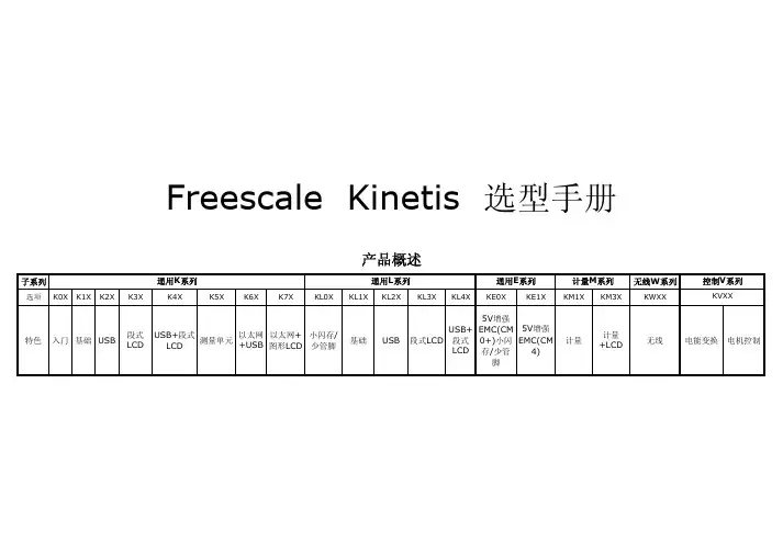
飞思卡尔半导体产品概述文档号: K10PBZHS 第2版, 2010年11月目录1Kinetis 产品组合Kinetis 是基于ARM® Cortex TM-M4具有超强可扩展性的低功耗、混合信号微控制器。
第一阶段产品由五个微控制器系列组成,包含超过两百种器件,在引脚、外设和软件上可兼容。
每个系列提供了不同的性能,存储器和外设特性。
通过通用外设、存储器映射和封装的一致性来实现系列内和各系列间的便捷移植。
Kinetis 微控制器基于飞思卡尔创新的90 纳米薄膜存储器(TFS)闪存技术,具有独特的Flex存储器(可配置的内嵌EEPROM)。
Kinetis 微控制器系列融合了最新的低功耗革新技术,具有高性能、高精度的混合信号能力,宽广的互连性,人机接口和安全外设。
飞思卡尔公司以及其他大量的ARM第三方应用商提供对Kinetis 微控制器的应用支持。
1Kinetis 产品组合 . . . . . . . . . . . . . . . . . 1 2K10系列介绍. . . . . . . . . . . . . . . . . . . 4 3K10模块结构图. . . . . . . . . . . . . . . . . . 4 4特性. . . . . . . . . . . . . . . . . . . . . . . 64.1K10系列MCU的共性. . . . . . . . . . . . . 64.2Flex存储器 . . . . . . . . . . . . . . . . . 74.3器件号和封装信息 . . . . . . . . . . . . . . 84.4K10系列特性 . . . . . . . . . . . . . . . 104.5模块特性 . . . . . . . . . . . . . . . . . 27 5功耗模式. . . . . . . . . . . . . . . . . . . . 37 6开发环境. . . . . . . . . . . . . . . . . . . . 386.1飞思卡尔的塔式系统 . . . . . . . . . . . . 386.2CodeWarrior开发组件 . . . . . . . . . . . 396.3飞思卡尔的MQX TM软件解决方案 . . . . . . 406.4额外提供的软件栈 . . . . . . . . . . . . . 42 7修订记录. . . . . . . . . . . . . . . . . . . . 42K10系列产品概述适用于所有K10微控制器Kinetis 产品组合图 1. Kenetis微控制器产品组合所有的 Kinetis系列包含丰富的模拟、通信和定时控制外设,提供多种闪存容量和输入输出引脚数量。
Freescale Kinetis KL25系列社区资料大全及实例汇总介绍:Freescale 公司Kinetis KL25 MCU向L系列内增加了带集成低压稳压器的全速USB 2.0 OTG控制器,采用32位ARM Cortex-M0内核,拥有48MHz内核频率,工作电压为1.71V~3.6V,。
KL25系列作为低功耗、低价格、高性能的微控制器,给工程师们提供了一个合适的入门级32位方案。
本文精选了Kinetis K25教程、例程、设计案例,以及基于Kinetis KL25的流行开发板,集结了国内外官方资料和资深工程师的经验,是学习Kinetis KL25 MCU的必备宝典。
Kinetis KL25 MCU 的功能框图Kinetis KL25 MCU 教程篇Kinetis KL25 MCU官方参考手册Kinetis KL25 MCU 官方数据手册飞思卡尔Kinetis系列产品开发资源链接总汇包含Kinetis系列产品的参考手册、数据手册、编译环境、调试工具的相关资源链接。
KL25中文用户手册官方Kinetis L系列三大特性演示视频(附中文说明文档)你在设计中往往会忽略掉Kinetis L系列的重要的特性。
如果你只是简单的把Kinetis L系列当做一般的Cortex-M0的单片机来使用的话,我们的设计人员估计要郁闷了。
闲话少说,赶紧来看看你可能忽略的特性吧Cortex-M0+, 到底“+”了什么(有视频,有中文文档)飞思卡尔Kinetis L系列采用的内核是Cortex-M0+,而不是Cortex-M0。
这个小小的加号到底增加了什么呢?小小视频讲的一清二楚。
根据KL系列芯片上的缩略标志识别具体型号大家在使用kinetis芯片的时候,可能会发现一些比较小的芯片上并没有刻出芯片的具体型号,而是刻了一个缩略型号名称,那么如何根据这个缩略名称来识别具体的型号呢?文中罗列了Kinetis L系列所有的缩略型号对应的芯片具体型号名称,方便大家识别。
低功耗10位100 MHz流水线AD转换器设计时间:2010-11-16 09:07:50 来源:现代电子技术作者:贺炜西安邮电学院摘要:介绍了一个10位100 MHz,1.8 V的流水线结构模/数转换器(ADC),该ADC运用相邻级运算放大器共享技术和逐级电容缩减技术,可以大大减小芯片的功耗和面积。
电路采用级联1个高性能前置采样保持单元和4个运放共享的1.5位/级MDAC,并采用栅压自举开关和动态比较器来缩减功耗。
结果显示,在输入频率达到奈奎斯特频率范围内,整个ADC的有效位数始终高于9位。
电路使用TSMC O.18 μm 1P6M CMOS工艺,在100 MHz的采样频率下,功耗仅为45 mW。
关键词:流模/数转换器;运放共享;栅压自举开关;动态比较器O 引言在混合信号集成电路系统中,模/数转换器(ADC)是一个关键的模块。
许多现代应用,如数字便携设备、视频处理及无线通信等,都要求具有高采样率、低功耗的模/数转换器。
同时,由于许多模/数转换器被使用在电池供电的便携式设备中,降低其功耗就变得越加重要。
对于10 b,1 MSPS以上的ADC 系统而言,流水线结构是一种合适的设计方案。
在此阐述了能够满足10位精度、100 MHz采样率的流水线结构ADC,并且运用了相邻两级共用一个运放的运放共享技术和逐级电容缩减技术来减小功耗和面积。
该模/数转换器中采用了低功耗增益提高运算放大器和动态比较器等元件,也更好的降低了功耗。
1 ADC电路结构1.5位/级结构的ADC具有许多优点,首先每级多产生一位冗余位来进行数字冗余修正,大大减小比较器失调造成的影响。
其次较小的单级分辨率可以获得较高的速度。
1.5位/级结构的单级闭环增益为2,开关电容电路可以具有较小的负载电容和反馈因子,因此每级可以获得较大的带宽。
所以本电路采用1.5位/级级联的结构。
图1为本文所采用的流水线ADC结构,采用了每级1.5位流水线级级联。
最前端是一个高性能采样保持电路,虽然采样保持电路需要消耗大量的功耗,但它能够较好地减小由于MDAC和子ADC之间的采样信号失配造成的孔径误差,可以使得电路性能得到较大提高。