J78 VHB V1.1
- 格式:pptx
- 大小:2.93 MB
- 文档页数:25
March 2010Doc ID 2143 Rev 211/58L78xx - L78xxC L78xxAB - L78xxACPositive voltage regulatorsFeatures■Output current up to 1.5 A■Output voltages of 5; 6; 8; 8.5; 9; 12; 15; 18; 24 V■Thermal overload protection ■Short circuit protection■Output transition SOA protection ■ 2 % output voltage tolerance (A version)■Guaranteed in extended temperature range (A version)DescriptionThe L78xx series of three-terminal positiveregulators is available in TO-220, TO-220FP , TO-3, D²PAK and DPAK packages and several fixed output voltages, making it useful in a wide range of applications. These regulators can provide local on-card regulation, eliminating thedistribution problems associated with single point regulation. Each type employs internal current limiting, thermal shut-down and safe areaprotection, making it essentially indestructible. If adequate heat sinking is provided, they candeliver over 1 A output current. Although designed primarily as fixed voltage regulators, thesedevices can be used with external components to obtain adjustable voltage and currents.Table 1.Device summaryPart numbersL7805L7806AC L7809AB L7815AB L7805C L7808C L7809AC L7815AC L7805AB L7808AB L7812C L7818C L7805AC L7808AC L7812AB L7824C L7806C L7885C L7812AC L7824AB L7806ABL7809CL7815CL7824ACContents L78xx, L78xxC, L78xxAB, L78xxACContents1Diagram . . . . . . . . . . . . . . . . . . . . . . . . . . . . . . . . . . . . . . . . . . . . . . . . . . . 6 2Pin configuration . . . . . . . . . . . . . . . . . . . . . . . . . . . . . . . . . . . . . . . . . . . 7 3Maximum ratings . . . . . . . . . . . . . . . . . . . . . . . . . . . . . . . . . . . . . . . . . . . . 8 4Test circuits . . . . . . . . . . . . . . . . . . . . . . . . . . . . . . . . . . . . . . . . . . . . . . . . 9 5Electrical characteristics . . . . . . . . . . . . . . . . . . . . . . . . . . . . . . . . . . . . 106Application information . . . . . . . . . . . . . . . . . . . . . . . . . . . . . . . . . . . . . 296.1Design consideration . . . . . . . . . . . . . . . . . . . . . . . . . . . . . . . . . . . . . . . . 29 7Typical performance . . . . . . . . . . . . . . . . . . . . . . . . . . . . . . . . . . . . . . . . 39 8Package mechanical data . . . . . . . . . . . . . . . . . . . . . . . . . . . . . . . . . . . . 41 9Order codes . . . . . . . . . . . . . . . . . . . . . . . . . . . . . . . . . . . . . . . . . . . . . . 56 10Revision history . . . . . . . . . . . . . . . . . . . . . . . . . . . . . . . . . . . . . . . . . . . 572/58Doc ID 2143 Rev 21L78xx, L78xxC, L78xxAB, L78xxAC List of tables List of tablesTable 1.Device summary. . . . . . . . . . . . . . . . . . . . . . . . . . . . . . . . . . . . . . . . . . . . . . . . . . . . . . . . . . 1 Table 2.Absolute maximum ratings. . . . . . . . . . . . . . . . . . . . . . . . . . . . . . . . . . . . . . . . . . . . . . . . . . 8 Table 3.Thermal data. . . . . . . . . . . . . . . . . . . . . . . . . . . . . . . . . . . . . . . . . . . . . . . . . . . . . . . . . . . . . 8 Table 4.Electrical characteristics of L7805 . . . . . . . . . . . . . . . . . . . . . . . . . . . . . . . . . . . . . . . . . . . 10 Table 5.Electrical characteristics of L7805A . . . . . . . . . . . . . . . . . . . . . . . . . . . . . . . . . . . . . . . . . . 11 Table 6.Electrical characteristics of L7806A . . . . . . . . . . . . . . . . . . . . . . . . . . . . . . . . . . . . . . . . . . 12 Table 7.Electrical characteristics of L7808A . . . . . . . . . . . . . . . . . . . . . . . . . . . . . . . . . . . . . . . . . . 13 Table 8.Electrical characteristics of L7809A . . . . . . . . . . . . . . . . . . . . . . . . . . . . . . . . . . . . . . . . . . 14 Table 9.Electrical characteristics of L7812A . . . . . . . . . . . . . . . . . . . . . . . . . . . . . . . . . . . . . . . . . . 15 Table 10.Electrical characteristics of L7815A . . . . . . . . . . . . . . . . . . . . . . . . . . . . . . . . . . . . . . . . . . 16 Table 11.Electrical characteristics of L7824A . . . . . . . . . . . . . . . . . . . . . . . . . . . . . . . . . . . . . . . . . . 17 Table 12.Electrical characteristics of L7805C . . . . . . . . . . . . . . . . . . . . . . . . . . . . . . . . . . . . . . . . . . 18 Table 13.Electrical characteristics of L7806C . . . . . . . . . . . . . . . . . . . . . . . . . . . . . . . . . . . . . . . . . . 19 Table 14.Electrical characteristics of L7808C . . . . . . . . . . . . . . . . . . . . . . . . . . . . . . . . . . . . . . . . . . 20 Table 15.Electrical characteristics of L7885C . . . . . . . . . . . . . . . . . . . . . . . . . . . . . . . . . . . . . . . . . . 21 Table 16.Electrical characteristics of L7809C . . . . . . . . . . . . . . . . . . . . . . . . . . . . . . . . . . . . . . . . . . 22 Table 17.Electrical characteristics of L7810C . . . . . . . . . . . . . . . . . . . . . . . . . . . . . . . . . . . . . . . . . . 23 Table 18.Electrical characteristics of L7812C . . . . . . . . . . . . . . . . . . . . . . . . . . . . . . . . . . . . . . . . . . 24 Table 19.Electrical characteristics of L7815C . . . . . . . . . . . . . . . . . . . . . . . . . . . . . . . . . . . . . . . . . . 25 Table 20.Electrical characteristics of L7818C . . . . . . . . . . . . . . . . . . . . . . . . . . . . . . . . . . . . . . . . . . 26 Table 21.Electrical characteristics of L7820C . . . . . . . . . . . . . . . . . . . . . . . . . . . . . . . . . . . . . . . . . . 27 Table 22.Electrical characteristics of L7824C . . . . . . . . . . . . . . . . . . . . . . . . . . . . . . . . . . . . . . . . . . 28 Table 23.TO-220 mechanical data . . . . . . . . . . . . . . . . . . . . . . . . . . . . . . . . . . . . . . . . . . . . . . . . . . 41 Table 24.TO-220FP mechanical data . . . . . . . . . . . . . . . . . . . . . . . . . . . . . . . . . . . . . . . . . . . . . . . . 46 Table 25.TO-3 mechanical data . . . . . . . . . . . . . . . . . . . . . . . . . . . . . . . . . . . . . . . . . . . . . . . . . . . . 47 Table 26.DPAK mechanical data. . . . . . . . . . . . . . . . . . . . . . . . . . . . . . . . . . . . . . . . . . . . . . . . . . . . 49 Table 27.Tape and reel DPAK mechanical data . . . . . . . . . . . . . . . . . . . . . . . . . . . . . . . . . . . . . . . . 50 Table 28.D²PAK mechanical data . . . . . . . . . . . . . . . . . . . . . . . . . . . . . . . . . . . . . . . . . . . . . . . . . . . 53 Table 29.D²PAK footprint data. . . . . . . . . . . . . . . . . . . . . . . . . . . . . . . . . . . . . . . . . . . . . . . . . . . . . . 54 Table 30.Tape and reel D²PAK mechanical data . . . . . . . . . . . . . . . . . . . . . . . . . . . . . . . . . . . . . . . 55 Table 31.Order codes . . . . . . . . . . . . . . . . . . . . . . . . . . . . . . . . . . . . . . . . . . . . . . . . . . . . . . . . . . . . 56 Table 32.Document revision history . . . . . . . . . . . . . . . . . . . . . . . . . . . . . . . . . . . . . . . . . . . . . . . . . 57Doc ID 2143 Rev 213/58List of figures L78xx, L78xxC, L78xxAB, L78xxAC List of figuresFigure 1.Block diagram. . . . . . . . . . . . . . . . . . . . . . . . . . . . . . . . . . . . . . . . . . . . . . . . . . . . . . . . . . . . 6 Figure 2.Pin connections (top view) . . . . . . . . . . . . . . . . . . . . . . . . . . . . . . . . . . . . . . . . . . . . . . . . . . 7 Figure 3.Schematic diagram. . . . . . . . . . . . . . . . . . . . . . . . . . . . . . . . . . . . . . . . . . . . . . . . . . . . . . . . 7 Figure 4.Application circuits . . . . . . . . . . . . . . . . . . . . . . . . . . . . . . . . . . . . . . . . . . . . . . . . . . . . . . . . 8 Figure 5.DC parameter. . . . . . . . . . . . . . . . . . . . . . . . . . . . . . . . . . . . . . . . . . . . . . . . . . . . . . . . . . . . 9 Figure 6.Load regulation. . . . . . . . . . . . . . . . . . . . . . . . . . . . . . . . . . . . . . . . . . . . . . . . . . . . . . . . . . . 9 Figure 7.Ripple rejection. . . . . . . . . . . . . . . . . . . . . . . . . . . . . . . . . . . . . . . . . . . . . . . . . . . . . . . . . . . 9 Figure 8.DC parameter. . . . . . . . . . . . . . . . . . . . . . . . . . . . . . . . . . . . . . . . . . . . . . . . . . . . . . . . . . . 29 Figure 9.DC parameter. . . . . . . . . . . . . . . . . . . . . . . . . . . . . . . . . . . . . . . . . . . . . . . . . . . . . . . . . . . 30 Figure 10.DC parameter. . . . . . . . . . . . . . . . . . . . . . . . . . . . . . . . . . . . . . . . . . . . . . . . . . . . . . . . . . . 30 Figure 11.DC parameter. . . . . . . . . . . . . . . . . . . . . . . . . . . . . . . . . . . . . . . . . . . . . . . . . . . . . . . . . . . 30 Figure 12.Fixed output regulator. . . . . . . . . . . . . . . . . . . . . . . . . . . . . . . . . . . . . . . . . . . . . . . . . . . . . 31 Figure 13.Current regulator. . . . . . . . . . . . . . . . . . . . . . . . . . . . . . . . . . . . . . . . . . . . . . . . . . . . . . . . . 31 Figure 14.Circuit for increasing output voltage. . . . . . . . . . . . . . . . . . . . . . . . . . . . . . . . . . . . . . . . . . 31 Figure 15.Adjustable output regulator (7 to 30 V). . . . . . . . . . . . . . . . . . . . . . . . . . . . . . . . . . . . . . . . 32 Figure 16.0.5 to 10 V regulator. . . . . . . . . . . . . . . . . . . . . . . . . . . . . . . . . . . . . . . . . . . . . . . . . . . . . . 32 Figure 17.High current voltage regulator . . . . . . . . . . . . . . . . . . . . . . . . . . . . . . . . . . . . . . . . . . . . . . 32 Figure 18.High output current with short circuit protection . . . . . . . . . . . . . . . . . . . . . . . . . . . . . . . . . 33 Figure 19.Tracking voltage regulator . . . . . . . . . . . . . . . . . . . . . . . . . . . . . . . . . . . . . . . . . . . . . . . . . 33 Figure 20.Split power supply (± 15 V - 1 A) . . . . . . . . . . . . . . . . . . . . . . . . . . . . . . . . . . . . . . . . . . . . 34 Figure 21.Negative output voltage circuit . . . . . . . . . . . . . . . . . . . . . . . . . . . . . . . . . . . . . . . . . . . . . . 34 Figure 22.Switching regulator. . . . . . . . . . . . . . . . . . . . . . . . . . . . . . . . . . . . . . . . . . . . . . . . . . . . . . . 34 Figure 23.High input voltage circuit. . . . . . . . . . . . . . . . . . . . . . . . . . . . . . . . . . . . . . . . . . . . . . . . . . . 35 Figure 24.High input voltage circuit. . . . . . . . . . . . . . . . . . . . . . . . . . . . . . . . . . . . . . . . . . . . . . . . . . . 35 Figure 25.High output voltage regulator . . . . . . . . . . . . . . . . . . . . . . . . . . . . . . . . . . . . . . . . . . . . . . . 35 Figure 26.High input and output voltage. . . . . . . . . . . . . . . . . . . . . . . . . . . . . . . . . . . . . . . . . . . . . . . 36 Figure 27.Reducing power dissipation with dropping resistor. . . . . . . . . . . . . . . . . . . . . . . . . . . . . . . 36 Figure 28.Remote shutdown. . . . . . . . . . . . . . . . . . . . . . . . . . . . . . . . . . . . . . . . . . . . . . . . . . . . . . . . 36 Figure 29.Power AM modulator (unity voltage gain, IO £ 0.5) . . . . . . . . . . . . . . . . . . . . . . . . . . . . . . 37 Figure 30.Adjustable output voltage with temperature compensation . . . . . . . . . . . . . . . . . . . . . . . . 37 Figure 31.Light controllers (VO(min) = VXX + VBE). . . . . . . . . . . . . . . . . . . . . . . . . . . . . . . . . . . . . . 38 Figure 32.Protection against input short-circuit with high capacitance loads . . . . . . . . . . . . . . . . . . . 38 Figure 33.Dropout voltage vs. junction temperature. . . . . . . . . . . . . . . . . . . . . . . . . . . . . . . . . . . . . . 39 Figure 34.Peak output current vs. input/output differential voltage. . . . . . . . . . . . . . . . . . . . . . . . . . . 39 Figure 35.Supply voltage rejection vs. frequency. . . . . . . . . . . . . . . . . . . . . . . . . . . . . . . . . . . . . . . . 39 Figure 36.Output voltage vs. junction temperature. . . . . . . . . . . . . . . . . . . . . . . . . . . . . . . . . . . . . . . 39 Figure 37.Output impedance vs. frequency . . . . . . . . . . . . . . . . . . . . . . . . . . . . . . . . . . . . . . . . . . . . 39 Figure 38.Quiescent current vs. junction temp. . . . . . . . . . . . . . . . . . . . . . . . . . . . . . . . . . . . . . . . . . 39 Figure 39.Load transient response. . . . . . . . . . . . . . . . . . . . . . . . . . . . . . . . . . . . . . . . . . . . . . . . . . . 40 Figure 40.Line transient response . . . . . . . . . . . . . . . . . . . . . . . . . . . . . . . . . . . . . . . . . . . . . . . . . . . 40 Figure 41.Quiescent current vs. input voltage . . . . . . . . . . . . . . . . . . . . . . . . . . . . . . . . . . . . . . . . . . 40 Figure 42.Drawing dimension TO-220 (type STD-ST Dual Gauge) . . . . . . . . . . . . . . . . . . . . . . . . . . 42 Figure 43.Drawing dimension TO-220 (type STD-ST Single Gauge). . . . . . . . . . . . . . . . . . . . . . . . . 43 Figure 44.Drawing dimension tube for TO-220 Dual Gauge (mm.) . . . . . . . . . . . . . . . . . . . . . . . . . . 44 Figure 45.Drawing dimension tube for TO-220 Single Gauge (mm.) . . . . . . . . . . . . . . . . . . . . . . . . . 44 Figure 46.Drawing dimension TO-220FP. . . . . . . . . . . . . . . . . . . . . . . . . . . . . . . . . . . . . . . . . . . . . . 45 Figure 47.Drawing dimension TO-3 . . . . . . . . . . . . . . . . . . . . . . . . . . . . . . . . . . . . . . . . . . . . . . . . . . 47 Figure 48.Drawing dimension DPAK . . . . . . . . . . . . . . . . . . . . . . . . . . . . . . . . . . . . . . . . . . . . . . . . . 48 Figure 49.Drawing dimension tape and reel for DPAK. . . . . . . . . . . . . . . . . . . . . . . . . . . . . . . . . . . . 50 Figure 50.Drawing dimension D²PAK (type STD-ST). . . . . . . . . . . . . . . . . . . . . . . . . . . . . . . . . . . . . 51 4/58Doc ID 2143 Rev 21L78xx, L78xxC, L78xxAB, L78xxAC List of figures Figure 51.Drawing dimension D²PAK (type WOOSEOK-Subcon.). . . . . . . . . . . . . . . . . . . . . . . . . . . 52 Figure 52.D²PAK footprint recommended data. . . . . . . . . . . . . . . . . . . . . . . . . . . . . . . . . . . . . . . . . . 54 Figure 53.Drawing dimension tape and reel for D²PAK . . . . . . . . . . . . . . . . . . . . . . . . . . . . . . . . . . . 55Doc ID 2143 Rev 215/58Diagram L78xx, L78xxC, L78xxAB, L78xxAC 1 Diagram6/58Doc ID 2143 Rev 21L78xx, L78xxC, L78xxAB, L78xxAC Pin configuration 2 Pin configurationDoc ID 2143 Rev 217/58Maximum ratings L78xx, L78xxC, L78xxAB, L78xxAC8/58Doc ID 2143 Rev 213 Maximum ratingsNote:Absolute maximum ratings are those values beyond which damage to the device may occur.Functional operation under these condition is not implied.Table 2.Absolute maximum ratingsSymbol ParameterValue Unit V I DC input voltage for V O = 5 to 18 V 35Vfor V O = 20, 24 V40I O Output current Internally limited P D Power dissipationInternally limited T STGStorage temperature range-65 to 150°C T OPOperating junction temperature range for L78xx-55 to 150°C for L78xxC, L78xxAC0 to 125for L78xxAB-40 to 125Table 3.Thermal dataSymbol ParameterD²PAKDPAK TO-220TO-220FPTO-3Unit R thJC Thermal resistance junction-case 38554°C/W R thJAThermal resistance junction-ambient62.5100506035°C/WL78xx, L78xxC, L78xxAB, L78xxAC Test circuitsDoc ID 2143 Rev 219/584 Test circuitsElectrical characteristics L78xx, L78xxC, L78xxAB, L78xxAC10/58Doc ID 2143 Rev 215 Electrical characteristicsRefer to the test circuits, T J = -55 to 150 °C, V I = 10 V, I O = 500 mA, C I = 0.33 µF ,C O = 0.1 µF unless otherwise specified.Table 4.Electrical characteristics of L7805Symbol ParameterTest conditionsMin.Typ.Max.Unit V O Output voltage T J = 25°C4.855.2V V O Output voltage I O = 5 mA to 1 A, V I = 8 to 20 V 4.655 5.35V ΔV O (1)Line regulationV I = 7 to 25 V , T J = 25°C 350mVV I = 8 to 12 V , T J = 25°C 125ΔV O (1)Load regulation I O = 5 mA to 1.5 A, T J = 25°C 100mV I O = 250 to 750 mA, T J = 25°C 25I d Quiescent current T J = 25°C 6mA ΔI d Quiescent current change I O = 5 mA to 1 A 0.5mA V I = 8 to 25 V 0.8ΔV O /ΔT Output voltage drift I O = 5 mA0.6mV/°C eN Output noise voltage B =10 Hz to 100 kHz, T J = 25°C 40µV/V O SVR Supply voltage rejection V I = 8 to 18 V , f = 120 Hz 68dB V d Dropout voltage I O = 1 A, T J = 25°C 2 2.5V R O Output resistance f = 1 kHz17m ΩI sc Short circuit current V I = 35 V , T J = 25°C 0.75 1.2A I scpShort circuit peak currentT J = 25°C1.32.23.3A1.Load and line regulation are specified at constant junction temperature. Changes in V O due to heating effects must betaken into account separately. Pulse testing with low duty cycle is used.V I = 10 V, I O = 1 A, T J = 0 to 125 °C (L7805AC), T J = -40 to 125 °C (L7805AB), unlessotherwise specified.Table 5.Electrical characteristics of L7805ASymbol Parameter Test conditions Min.Typ.Max.Unit V O Output voltage T J = 25°C 4.95 5.1V V O Output voltage I O = 5 mA to 1 A, V I = 7.5 to 18 V 4.85 5.2V V O Output voltage I O = 1 A, V I = 18 to 20 V, T J = 25°C 4.85 5.2VΔV O (1)Line regulation V I = 7.5 to 25 V, I O = 500 mA750mV V I = 8 to 12 V1050mV V I = 8 to 12 V, T J = 25°C225mV V I = 7.3 to 20 V, T J = 25°C750mVΔV O (1)Load regulation I O = 5 mA to 1 A25100mV I O = 5 mA to 1.5 A, T J = 25°C30100V I O = 250 to 750 mA850VI q Quiescent current T J = 25°C 4.36mA6mAΔI q Quiescent current change V I = 8 to 23 V, I O = 500 mA0.8mA V I = 7.5 to 20 V, T J = 25°C0.8mA I O = 5 mA to 1 A0.5mASVR Supply voltage rejection V I = 8 to 18 V, f = 120 Hz, I O = 500 mA68dB V d Dropout voltage I O = 1 A, T J = 25°C2V eN Output noise voltage T A = 25°C, B =10 Hz to 100 kHz10µV/V O R O Output resistance f = 1 kHz17mΩI sc Short circuit current V I = 35 V, T A = 25°C0.2AI scp Short circuit peak current T J = 25°C 2.2AΔV O/ΔT Output voltage drift-1.1mV/°C 1.Load and line regulation are specified at constant junction temperature. Changes in V O due to heating effects must betaken into account separately. Pulse testing with low duty cycle is used.Doc ID 2143 Rev 2111/58V I = 11 V, I O = 1 A, TJ = 0 to 125 °C (L7806AC), T J = -40 to 125 °C (L7806AB), unlessotherwise specified.Table 6.Electrical characteristics of L7806ASymbol Parameter Test conditions Min.Typ.Max.Unit V O Output voltage T J = 25°C 5.886 6.12V V O Output voltage I O = 5 mA to 1 A, V I = 8.6 to 19 V 5.766 6.24V V O Output voltage I O = 1 A, V I = 19 to 21 V, T J = 25°C 5.766 6.24VΔV O (1)Line regulation V I = 8.6 to 25 V, I O = 500 mA960mV V I = 9 to 13 V1160mV V I = 9 to 13 V, T J = 25°C330mV V I = 8.3 to 21 V, T J = 25°C960mVΔV O (1)Load regulation I O = 5 mA to 1 A25100mV I O = 5 mA to 1.5 A, T J = 25°C30100V I O = 250 to 750 mA1050VI q Quiescent current T J = 25°C 4.36mA6mAΔI q Quiescent current change V I = 9 to 24 V, I O = 500 mA0.8mA V I = 8.6 to 21 V, T J = 25°C0.8mA I O = 5 mA to 1 A0.5mASVR Supply voltage rejection V I = 9 to 19 V, f = 120 Hz, I O = 500 mA65dB V d Dropout voltage I O = 1 A, T J = 25°C2V eN Output noise voltage T A = 25°C, B =10 Hz to 100 kHz10µV/V O R O Output resistance f = 1 kHz17mΩI sc Short circuit current V I = 35 V, T A = 25°C0.2AI scp Short circuit peak current T J = 25°C 2.2A ΔV O/ΔT Output voltage drift-0.8mV/°C 1.Load and line regulation are specified at constant junction temperature. Changes in V O due to heating effects must betaken into account separately. Pulse testing with low duty cycle is used.12/58Doc ID 2143 Rev 21V I = 14 V, I O = 1 A, TJ = 0 to 125 °C (L7808AC), T J = -40 to 125 °C (L7808AB), unlessotherwise specified.Table 7.Electrical characteristics of L7808ASymbol Parameter Test conditions Min.Typ.Max.Unit V O Output voltage T J = 25°C7.8488.16V V O Output voltage I O = 5 mA to 1 A, V I = 10.6 to 21 V7.788.3V V O Output voltage I O = 1 A, V I = 21 to 23 V, T J = 25°C7.788.3VΔV O (1)Line regulation V I = 10.6 to 25 V, I O = 500 mA1280mV V I = 11 to 17 V1580mV V I = 11 to 17 V, T J = 25°C540mV V I = 10.4 to 23 V, T J = 25°C1280mVΔV O (1)Load regulation I O = 5 mA to 1 A25100mV I O = 5 mA to 1.5 A, T J = 25°C30100V I O = 250 to 750 mA1050VI q Quiescent current T J = 25°C 4.36mA6mAΔI q Quiescent current change V I = 11 to 23 V, I O = 500 mA0.8mA V I = 10.6 to 23 V, T J = 25°C0.8mA I O = 5 mA to 1 A0.5mASVR Supply voltage rejection V I = 11.5 to 21.5 V, f = 120 Hz,I O = 500 mA62dBV d Dropout voltage I O = 1 A, T J = 25°C2V eN Output noise voltage T A = 25°C, B =10 Hz to 100 kHz10µV/V O R O Output resistance f = 1 kHz18mΩI sc Short circuit current V I = 35 V, T A = 25°C0.2AI scp Short circuit peak current T J = 25°C 2.2AΔV O/ΔT Output voltage drift-0.8mV/°C 1.Load and line regulation are specified at constant junction temperature. Changes in V O due to heating effects must betaken into account separately. Pulse testing with low duty cycle is used.Doc ID 2143 Rev 2113/58V I = 15 V, I O = 1 A, TJ = 0 to 125 °C (L7809AC), T J = -40 to 125 °C (L7809AB), unlessotherwise specified.Table 8.Electrical characteristics of L7809ASymbol Parameter Test conditions Min.Typ.Max.Unit V O Output voltage T J = 25°C8.8299.18V V O Output voltage I O = 5 mA to 1 A, V I = 10.6 to 22 V8.6599.35V V O Output voltage I O = 1 A, V I = 22 to 24 V, T J = 25°C8.6599.35VΔV O (1)Line regulation V I = 10.6 to 25 V, I O = 500 mA1290mV V I = 11 to 17 V1590mV V I = 11 to 17 V, T J = 25°C545mV V I = 10.4 to 23 V, T J = 25°C1290mVΔV O (1)Load regulation I O = 5 mA to 1 A25100mV I O = 5 mA to 1.5 A, T J = 25°C30100V I O = 250 to 750 mA1050VI q Quiescent current T J = 25°C 4.36mA6mAΔI q Quiescent current change V I = 11 to 25 V, I O = 500 mA0.8mA V I = 10.6 to 23 V, T J = 25°C0.8mA I O = 5 mA to 1 A0.5mASVR Supply voltage rejection V I = 11.5 to 21.5 V, f = 120 Hz,I O = 500 mA61dBV d Dropout voltage I O = 1 A, T J = 25°C2V eN Output noise voltage T A = 25°C, B =10 Hz to 100 kHz10µV/V O R O Output resistance f = 1 kHz18mΩI sc Short circuit current V I = 35 V, T A = 25°C0.2AI scp Short circuit peak current T J = 25°C 2.2A ΔV O/ΔT Output voltage drift-0.8mV/°C 1.Load and line regulation are specified at constant junction temperature. Changes in V O due to heating effects must betaken into account separately. Pulse testing with low duty cycle is used.14/58Doc ID 2143 Rev 21V I = 19 V, I O = 1 A, TJ = 0 to 125 °C (L7812AC), T J = -40 to 125 °C (L7812AB), unlessotherwise specified.Table 9.Electrical characteristics of L7812ASymbol Parameter Test conditions Min.Typ.Max.Unit V O Output voltage T J = 25°C11.751212.25V V O Output voltage I O = 5 mA to 1 A, V I = 14.8 to 25 V11.51212.5V V O Output voltage I O = 1 A, V I = 25 to 27 V, T J = 25°C11.51212.5VΔV O (1)Line regulation V I = 14.8 to 30 V, I O = 500 mA13120mV V I = 16 to 12 V16120mV V I = 16 to 12 V, T J = 25°C660mV V I = 14.5 to 27 V, T J = 25°C13120mVΔV O (1)Load regulation I O = 5 mA to 1 A25100mV I O = 5 mA to 1.5 A, T J = 25°C30100V I O = 250 to 750 mA1050VI q Quiescent current T J = 25°C 4.46mA6mAΔI q Quiescent current change V I = 15 to 30 V, I O = 500 mA0.8mA V I = 14.8 to 27 V, T J = 25°C0.8mA I O = 5 mA to 1 A0.5mASVR Supply voltage rejection V I = 15 to 25 V, f = 120 Hz, I O = 500 mA60dB V d Dropout voltage I O = 1 A, T J = 25°C2V eN Output noise voltage T A = 25°C, B = 10 Hz to 100 kHz10µV/V O R O Output resistance f = 1 kHz18mΩI sc Short circuit current V I = 35 V, T A = 25°C0.2AI scp Short circuit peak current T J = 25°C 2.2AΔV O/ΔT Output voltage drift-1mV/°C 1.Load and line regulation are specified at constant junction temperature. Changes in V O due to heating effects must betaken into account separately. Pulse testing with low duty cycle is used.Doc ID 2143 Rev 2115/58V I = 23 V, I O = 1 A, TJ = 0 to 125 °C (L7815AC), T J = -40 to 125 °C (L7815AB), unlessotherwise specified.Table 10.Electrical characteristics of L7815ASymbol Parameter Test conditions Min.Typ.Max.Unit V O Output voltage T J = 25°C14.71515.3V V O Output voltage I O = 5 mA to 1 A, V I = 17.9 to 28 V14.41515.6V V O Output voltage I O = 1 A, V I = 28 to 30 V, T J = 25°C14.41515.6VΔV O (1)Line regulation V I = 17.9 to 30 V, I O = 500 mA13150mV V I = 20 to 26 V16150mV V I = 20 to 26 V, T J = 25°C675mV V I = 17.5 to 30 V, T J = 25°C13150mVΔV O (1)Load regulation I O = 5 mA to 1 A25100mV I O = 5 mA to 1.5 A, T J = 25°C30100V I O = 250 to 750 mA1050VI q Quiescent current T J = 25°C 4.46mA6mAΔI q Quiescent current change V I = 17.5 to 30 V, I O = 500 mA0.8mA V I = 17.5 to 30 V, T J = 25°C0.8mA I O = 5 mA to 1 A0.5mASVR Supply voltage rejection V I = 18.5 to 28.5 V, f = 120 Hz,I O = 500 mA58dBV d Dropout voltage I O = 1 A, T J = 25°C2V eN Output noise voltage T A = 25°C, B = 10Hz to 100 kHz10µV/V O R O Output resistance f = 1 kHz19mΩI sc Short circuit current V I = 35 V, T A = 25°C0.2AI scp Short circuit peak current T J = 25°C 2.2A ΔV O/ΔT Output voltage drift-1mV/°C 1.Load and line regulation are specified at constant junction temperature. Changes in V O due to heating effects must betaken into account separately. Pulse testing with low duty cycle is used.16/58Doc ID 2143 Rev 21V I = 33 V, I O = 1 A, TJ = 0 to 125 °C (L7824AC), T J = -40 to 125 °C (L7824AB), unlessotherwise specified.Table 11.Electrical characteristics of L7824ASymbol Parameter Test conditions Min.Typ.Max.Unit V O Output voltage T J = 25°C23.52424.5V V O Output voltage I O = 5 mA to 1 A, V I = 27.3 to 37 V232425V V O Output voltage I O = 1 A, V I = 37 to 38 V, T J = 25°C232425VΔV O (1)Line regulation V I = 27 to 38 V, I O = 500 mA31240mV V I = 30 to 36 V35200mV V I = 30 to 36 V, T J = 25°C14120mV V I = 26.7 to 38 V, T J = 25°C31240mVΔV O (1)Load regulation I O = 5 mA to 1 A25100mV I O = 5 mA to 1.5 A, T J = 25°C30100V I O = 250 to 750 mA1050VI q Quiescent current T J = 25°C 4.66mA6mAΔI q Quiescent current change V I = 27.3 to 38 V, I O = 500 mA0.8mA V I = 27.3 to 38 V, T J = 25°C0.8mA I O = 5 mA to 1 A0.5mASVR Supply voltage rejection V I = 28 to 38 V, f = 120 Hz, I O = 500 mA54dB V d Dropout voltage I O = 1 A, T J = 25°C2V eN Output noise voltage T A = 25°C, B = 10 Hz to 100 kHz10µV/V O R O Output resistance f = 1 kHz20mΩI sc Short circuit current V I = 35 V, T A = 25°C0.2AI scp Short circuit peak current T J = 25°C 2.2AΔV O/ΔT Output voltage drift-1.5mV/°C 1.Load and line regulation are specified at constant junction temperature. Changes in V O due to heating effects must betaken into account separately. Pulse testing with low duty cycle is used.Doc ID 2143 Rev 2117/58Refer to the test circuits, T J = 0 to 125 °C, V I = 10 V, I O = 500 mA, C I = 0.33 µF, C O = 0.1 µFunless otherwise specified.Table 12.Electrical characteristics of L7805CSymbol Parameter Test conditions Min.Typ.Max.Unit V O Output voltage T J = 25°C 4.85 5.2V V O Output voltage I O = 5 mA to 1 A, V I = 7 to 18 V 4.755 5.25V V O Output voltage I O = 1 A, V I = 18 to 20V, T J = 25°C 4.755 5.25VΔV O(1)Line regulation V I = 7 to 25 V, T J = 25°C3100mV V I = 8 to 12 V, T J = 25°C150ΔV O(1)Load regulation I O = 5 mA to 1.5 A, T J = 25°C100mV I O = 250 to 750 mA, T J = 25°C50I d Quiescent current T J = 25°C8mAΔI d Quiescent current change I O = 5 mA to 1 A0.5mA V I = 7 to 23 V0.8ΔV O/ΔT Output voltage drift I O = 5 mA-1.1mV/°C eN Output noise voltage B = 10 Hz to 100 kHz, T J = 25°C40µV/V O SVR Supply voltage rejection V I = 8 to 18 V, f = 120 Hz62dB V d Dropout voltage I O = 1 A, T J = 25°C2V R O Output resistance f = 1 kHz17mΩI sc Short circuit current V I = 35 V, T J = 25°C0.75AI scp Short circuit peak current T J = 25°C 2.2A1.Load and line regulation are specified at constant junction temperature. Changes in V O due to heating effects must betaken into account separately. Pulse testing with low duty cycle is used.18/58Doc ID 2143 Rev 21。
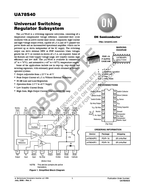
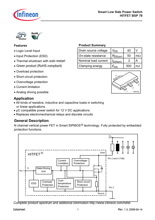
LM78S40Universal Switching Regulator SubsystemGeneral DescriptionThe LM78S40is a monolithic regulator subsystem consisting of all the active building blocks necessary for switching regu-lator systems.The device consists of a temperature com-pensated voltage reference,a duty-cycle controllable oscilla-tor with an active current limit circuit,an error amplifier,high current,high voltage output switch,a power diode and an uncommitted operational amplifier.The device can drive ex-ternal NPN or PNP transistors when currents in excess of 1.5A or voltages in excess of 40V are required.The device can be used for step-down,step-up or inverting switching regulators as well as for series pass regulators.It features wide supply voltage range,low standby power dissipation,high efficiency and low drift.It is useful for any stand-alone,low part count switching system and works extremely well in battery operated systems.Featuresn Step-up,step-down or inverting switching regulators n Output adjustable from 1.25V to 40Vn Peak currents to 1.5A without external transistors n Operation from 2.5V to 40V input n Low standby current drain n 80dB line and load regulationn High gain,high current,independent op amp nPulse width modulation with no double pulsingBlock and Connection DiagramsDS010057-216-Lead DIPDS010057-1Top ViewApril 1998LM78S40Universal Switching Regulator Subsystem©1998National Semiconductor Corporation Ordering InformationPart Number NS Package Temperature Range LM78S40J/883J16A Ceramic DIP−55˚C to+125˚C LM78S40N N16E Molded DIP−40˚C to+125˚C LM78S40CN N16E Molded DIP0˚C to+70˚C2Absolute Maximum Ratings(Note1)If Military/Aerospace specified devices are required, please contact the National Semiconductor Sales Office/ Distributors for availability and specifications.Storage Temperature RangeCeramic DIP−65˚C to+175˚C Molded DIP−65˚C to+150˚C Operating Temperature RangeExtended(LM78S40J)−55˚C to+125˚C Industrial(LM78S40N)−40˚C to+125˚C Commercial(LM78S40CN)0˚C to+70˚C Lead TemperatureCeramic DIP(Soldering,60sec.)300˚C Molded DIP(Soldering,10sec.)265˚C Internal Power Dissipation(Note2)(Note3)16L-Ceramic DIP 1.50W 16L-Molded DIP 1.04W Input Voltage from V IN to GND40V Input Voltage from V+(Op Amp)to GND40V Common Mode Input Range(Comparator and Op Amp)−0.3to V+ Differential Input Voltage(Note4)±30V Output Short CircuitDuration(Op Amp)Continuous Current from V REF10mA Voltage from SwitchCollectors to GND40V Voltage from SwitchEmitters to GND40V Voltage from SwitchCollectors to Emitter40V Voltage from Power Diode to GND40V Reverse Power Diode Voltage40V Current through Power Switch 1.5A Current through Power Diode 1.5A ESD Susceptibility(to be determined)LM78S40Electrical Characteristics(Note5)T A=Operating temperature range,V IN=5.0V,V+(Op Amp)=5.0V,unless otherwise specified.Symbol Parameter Conditions Min Typ Max Units GENERAL CHARACTERISTICSI CC Supply Current V IN=5.0V 1.8 3.5mA(Op Amp Disconnected)V IN=40V 2.3 5.0mAI CC Supply Current V IN=5.0V 4.0mA(Op Amp Connected)V IN=40V 5.5mA REFERENCE SECTIONV REF Reference Voltage I REF=1.0mA Extend−55˚C<T A<+125˚C,Comm0<T A<+70˚C, 1.180 1.245 1.310VIndus−40˚C<T A<+85˚CV R LINE Reference Voltage V IN=3.0V to V IN=40V,0.040.2mV/V Line Regulation I REF=1.0mA,T A=25˚CV R LOAD Reference Voltage I REF=1.0mA to I REF=10mA,0.20.5mV/mA Load Regulation T A=25˚COSCILLATOR SECTIONI CHG Charging Current V IN=5.0V,T A=25˚C2050µAI CHG Charging Current V IN=40V,T A=25˚C2070µAI DISCHG Discharge Current V IN=5.0V,T A=25˚C150250µAI DISCHG Discharge Current V IN=40V,T A=25˚C150350µAV OSC Oscillator Voltage Swing V IN=5.0V,T A=25˚C0.5Vt on/t off Ratio of Charge/ 6.0µs/µs Discharge TimeCURRENT LIMIT SECTIONV CLS Current Limit SenseVoltageT A=25˚C250350mV OUTPUT SWITCH SECTIONV SAT1Output Saturation Voltage1I SW=1.0A(Figure1) 1.1 1.3VV SAT2Output Saturation Voltage2I SW=1.0A(Figure2)0.450.7VLM78S40Electrical Characteristics(Note5)(Continued)T A=Operating temperature range,V IN=5.0V,V+(Op Amp)=5.0V,unless otherwise specified.Symbol Parameter Conditions Min Typ Max Units OUTPUT SWITCH SECTIONh FE Output Transistor CurrentI C=1.0A,V CE=5.0V,T A=25˚C70GainI L Output Leakage Current V O=40V,T A=25˚C10nA POWER DIODEV FD Forward Voltage Drop I D=1.0A 1.25 1.5V I DR Diode Leakage Current V D=40V,T A=25˚C10nA COMPARATORV IO Input Offset Voltage V CM=V REF 1.515mV I IB Input Bias Current V CM=V REF35200nA I IO Input Offset Current V CM=V REF 5.075nA V CM Common Mode VoltageT A=25˚C0V IN–2V RangeV IN=3.0V to40V,T A=25˚C7096dB PSRR Power Supply RejectionRatioOPERATIONAL AMPLIFIERV IO Input Offset Voltage V CM=2.5V 4.015mV I IB Input Bias Current V CM=2.5V30200nA I IO Input Offset Current V CM=2.5V 5.075nA A VS+Voltage Gain+R L=2.0kΩto GND;25250V/mVV O=1.0V to2.5V,T A=25˚CA VS−Voltage Gain−R L=2.0kΩto V+(Op Amp)25250V/mVV O=1.0V to2.5V,T A=25˚CV CM Common Mode VoltageT A=25˚C0V CC−2V RangeCMR Common Mode Rejection V CM=0V to3.0V,T A=25˚C76100dB PSRR Power Supply RejectionV+(Op Amp)=3.0V to40V,T A=25˚C76100dB RatioI O+Output Source Current T A=25˚C75150mA I O−Output Sink Current T A=25˚C1035mA SR Slew Rate T A=25˚C0.6V/µs V OL Output Voltage LOW I L=−5.0mA,T A=25˚C 1.0V V OH Output Voltage High I L=50mA,T A=25˚C V+(Op VAmp)−3VNote1:Absolute Maximum Ratings indicate limits beyond which damage to the device may occur.Electrical specifications do not apply when ordering the device beyond its rated operating conditions.Note2:T J Max=150˚C for the Molded DIP,and175˚C for the Ceramic DIP.Note3:Ratings apply to ambient temperature at25˚C.Above this temperature,derate the16L-Ceramic DIP at10mW/˚C,and the16L-Molded DIP at8.3mW/˚C.Note4:For supply voltages less than30V,the absolute maximum voltage is equal to the supply voltage.Note5:A military RETS specification is available on request.At the time of printing,the LM78S40RETS specification complied with the Min and Max limits in this table.The LM78S40J may also be procured as a Standard Military Drawing.4Typical Performance CharacteristicsDesign FormulasCharacteristic Step-Down Step-Up Inverting UnitsFunctional DescriptionSWITCHING FREQUENCY CONTROLThe LM78S40is a variable frequency,variable duty cycle device.The initial switching frequency is set by the timing capacitor.(Oscillator frequency is set by a single external capacitor and may be varied over a range of100Hz to 100kHz).The initial duty cycle is6:1.This switching fre-quency and duty cycle can be modified by two mechanisms—the current limit circuitry(I pk sense)and the comparator.The comparator modifies the OFF time.When the output voltage is correct,the comparator output is in the HIGH state and has no effect on the circuit operation.If the out-put voltage is too high then the comparator output goes LOW.In the LOW state the comparator inhibits the turn-on of the output stage switching transistors.As long as the comparator is LOW the system is in OFF time.As the out-put current rises the OFF time decreases.As the output current nears its maximum the OFF time approaches its minimum value.The comparator can inhibit several ON cycles,one ON cycle or any portion of an ON cycle.Once the ON cycle has begun the comparator cannot inhibit un-til the beginning of the next ON cycle.The current limit modifies the ON time.The current limit is activated when a300mV potential appears between lead 13(V CC)and lead14(I pk).This potential is intended to re-sult when designed for peak current flows through R SC. When the peak current is reached the current limit is turned on.The current limit circuitry provides for a quick end to ON time and the immediate start of OFF time. Generally the oscillator is free running but the current limit action tends to reset the timing cycle.Increasing load results in more current limited ON time and less OFF time.The switching frequency increases with load current.USING THE INTERNAL REFERENCE,DIODE,AND SWITCHThe internal1.245V reference(pin8)must be bypassed, with0.1µF directly to the ground pin(pin11)of the LM78S40,to assure its stability.V FD is the forward voltage drop across the internal power diode.It is listed on the data sheet as1.25V typical,1.5V maximum.If an external diode is used,then its own for-ward voltage drop must be used for V FD.V SAT is the voltage across the switch element(output tran-sistors Q1and Q2)when the switch is closed or ON.This is listed on the data sheet as Output Saturation Voltage.“Output saturation voltage1”is defined as the switching element voltage for Q2and Q1in the Darlington configu-ration with collectors tied together.This applies to Figure 1,the step down mode.“Output saturation voltage2”is the switching element volt-age for Q1only when used as a transistor switch.This ap-plies to Figure2,the step up mode.For the inverting mode,Figure3,the saturation voltage of the external transistor should be used for V SAT.Typical ApplicationsCharacteristic Condition TypicalValue Output Voltage I O=200mA10V Line Regulation20V≤V I≤30V 1.5mV Load Regulation 5.0mA≤I O 3.0mVI O≤300mAMax Output Current V O=9.5V500mA Output Ripple I O=200mA50mV Efficiency I O=200mA74% Standby Current I O=200mA 2.8mA Note7:For I O≥200mA use external diode to limit on-chip power dissipation.DS010057-3 FIGURE1.Typical Step-Down Regulator andOperational Performance(T A=25˚C)6Typical Applications(Continued)Characteristic Condition TypicalValue Output Voltage I O=50mA25V Line Regulation 5.0V≤V I≤15V 4.0mV Load Regulation 5.0mA≤I O 2.0mVI O≤100mAMax Output Current V O=23.75V160mA Output Ripple I O=50mA30mV Efficiency I O=50mA79% Standby Current I O=50mA 2.6mACharacteristic Condition TypicalValue Output Voltage I O=100mA−15V Line Regulation8.0V≤V I≤18V 5.0mV Load Regulation 5.0mA≤I O 3.0mVI O≤150mAMax Output Current V O=14.25V160mA Output Ripple I O=100mA20mV Efficiency I O=100mA70% Standby Current I O=100mA 2.3mADS010057-4FIGURE2.Typical Step-Up Regulator and Operational Performance(T A=25˚C)DS010057-5FIGURE3.Typical Inverting Regulator andOperational Performance(T A=25˚C)Typical Applications(Continued)DS010057-10 FIGURE4.Pulse Width Modulated Step-Down Regulator(f OSC=20kHz)8Physical Dimensions inches(millimeters)unless otherwise noted16-Lead Ceramic Dual-In-Line Package(J)Order Number LM78S40J/883NS Package Number J16A16-Lead Molded Dual-In-Line Package(N)Order Number LM78S40N or LM78S40CNNS Package Number N16ALIFE SUPPORT POLICYNATIONAL’S PRODUCTS ARE NOT AUTHORIZED FOR USE AS CRITICAL COMPONENTS IN LIFE SUPPORT DE-VICES OR SYSTEMS WITHOUT THE EXPRESS WRITTEN APPROVAL OF THE PRESIDENT OF NATIONAL SEMI-CONDUCTOR CORPORATION.As used herein:1.Life support devices or systems are devices or sys-tems which,(a)are intended for surgical implant intothe body,or (b)support or sustain life,and whose fail-ure to perform when properly used in accordancewith instructions for use provided in the labeling,can be reasonably expected to result in a significant injury to the user.2.A critical component in any component of a life support device or system whose failure to perform can be rea-sonably expected to cause the failure of the life support device or system,or to affect its safety or effectiveness.National Semiconductor Corporation AmericasTel:1-800-272-9959Fax:1-800-737-7018Email:support@National Semiconductor EuropeFax:+49(0)180-5308586Email:europe.support@Deutsch Tel:+49(0)180-5308585English Tel:+49(0)180-5327832Français Tel:+49(0)180-5329358Italiano Tel:+49(0)180-5341680National Semiconductor Asia Pacific Customer Response Group Tel:65-2544466Fax:65-2504466Email:sea.support@National Semiconductor Japan Ltd.Tel:81-3-5620-6175Fax:81-3-5620-6179L M 78S 40U n i v e r s a l S w i t c h i n g R e g u l a t o r S u b s y s t e mNational does not assume any responsibility for use of any circuitry described,no circuit patent licenses are implied and National reserves the right at any time without notice to change said circuitry and specifications.。
原版操作手册的译本1关于本文件适用文件产品所有相关文档è /pk。
–电机操作指南–轴操作指南2安全2.1安全注意事项–仅允许将产品安装在处于安全状态的部件上。
–清洁轴/空心轴。
联轴器只有夹紧在干燥且无润滑脂的轴表面上时才不会打滑。
–清洁 [1] 联轴器轮毂:–去除 [G] 外径夹紧销上的油脂。
为膨胀心轴椎体 [H] 润滑。
–去除夹紧孔的油脂。
–遵守 [1] 联轴器轮毂校准è 4.3.4 联轴器校准。
–为以下组合提供支撑è 4.4.1 轴-电机组合的支撑:–凸出的电机附件和重电机附件–强烈振动和振动/冲击负载–在每次松开或旋转电机后,进行轴的参照点运行。
–选择所需的紧固件。
该组件包括最大要求的紧固件。
–遵守拧紧力矩。
如果没有特别说明,则公差为 ± 20 %。
è 6 技术数据。
2.2按规定使用2.2.1使用轴与电机连接,电机与驱动轴呈轴向布置。
2.2.2许用的轴和电机过载将导致功能故障和财产损失。
电机的输出端变量不得超过所使用部件的许用数值。
许用数值è /catalogue。
•对电机输出端变量予以相应限制。
•由接口代码推导出轴和电机。
示例:EAMM-A-L48-70AL48:轴接口70A:电机接口轴接口轴1)L27EGC-50-...-TBL62EGC-120-...-TBN38ELGA-TB-...-70N48ELGA-TB-...-801) 齿形带式电缸 EGC/ELGATab. 1电机接口电机1)40A EMMS-AS-4040R外厂电机40RA外厂电机57AA外厂电机57AB外厂电机57AC外厂电机58AA外厂电机60PA外厂电机电机接口电机1)60RA外厂电机60RB外厂电机70AA外厂电机70AB外厂电机80P EMMB/EMME/EMMT-AS-80, 外厂电机84AA外厂电机88A外厂电机90R外厂电机92RA外厂电机1) 伺服电机 EMM...-ASTab. 2用户应自行决定将外厂电机与合适的机械接口进行组合。