降压开关稳压器LM2596系列的数据
- 格式:pdf
- 大小:522.41 KB
- 文档页数:4

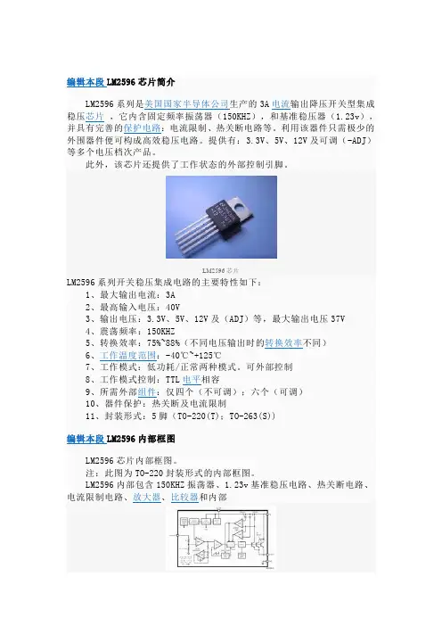
编辑本段LM2596芯片简介LM2596系列是美国国家半导体公司生产的3A电流输出降压开关型集成稳压芯片,它内含固定频率振荡器(150KHZ),和基准稳压器(1.23v),并具有完善的保护电路:电流限制、热关断电路等。
利用该器件只需极少的外围器件便可构成高效稳压电路。
提供有:3.3V、5V、12V及可调(-ADJ)等多个电压档次产品。
此外,该芯片还提供了工作状态的外部控制引脚。
LM2596芯片LM2596系列开关稳压集成电路的主要特性如下:1、最大输出电流:3A2、最高输入电压:40V3、输出电压:3.3V、5V、12V及(ADJ)等,最大输出电压37V4、震荡频率:150KHZ5、转换效率:75%~88%(不同电压输出时的转换效率不同)6、工作温度范围:-40℃~+125℃7、工作模式:低功耗/正常两种模式。
可外部控制8、工作模式控制:TTL电平相容9、所需外部组件:仅四个(不可调);六个(可调)10、器件保护:热关断及电流限制11、封装形式:5脚(TO-220(T);TO-263(S))编辑本段LM2596内部框图LM2596芯片内部框图。
注:此图为TO-220封装形式的内部框图。
LM2596内部包含150KHZ振荡器、1.23v基准稳压电路、热关断电路、电流限制电路、放大器、比较器和内部[1]稳压电路等。
为了产生不同的输出电压通常将比较器的负端接基准电压(1.23V ),正端接分压电阻网络。
其中R1=1KΩ,R2分别为1.7KΩ(3.3v),3.1KΩ(5V),8.8KΩ(12V)、0(-ADJ)。
将输出电压的分压电阻网络的输出同内部基准稳压值1.23V进行比较,若电压有偏差,则可用放大器控制内部振荡器的输出占空比,从而使输出电压保持稳定。
编辑本段LM2596经典应用实例具体应用时可根据需要选择:LM2596-5V、LM2596-3.3等。
要获得+1.8V、+5V输出电压时请选用A图,要获得+3.3V输出电压时请选用B图。
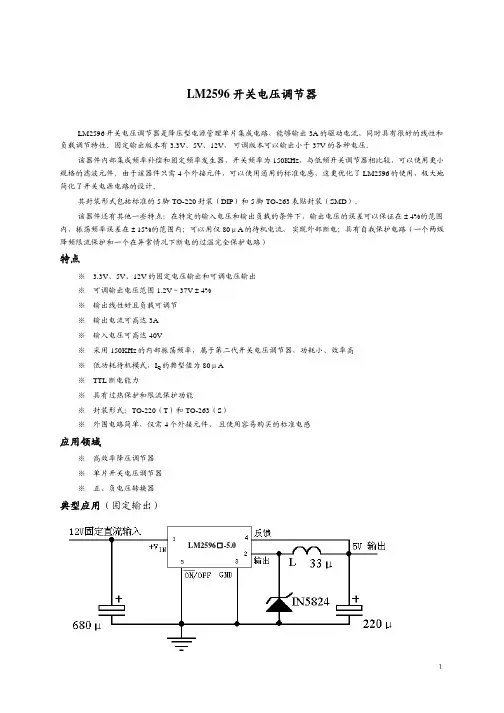
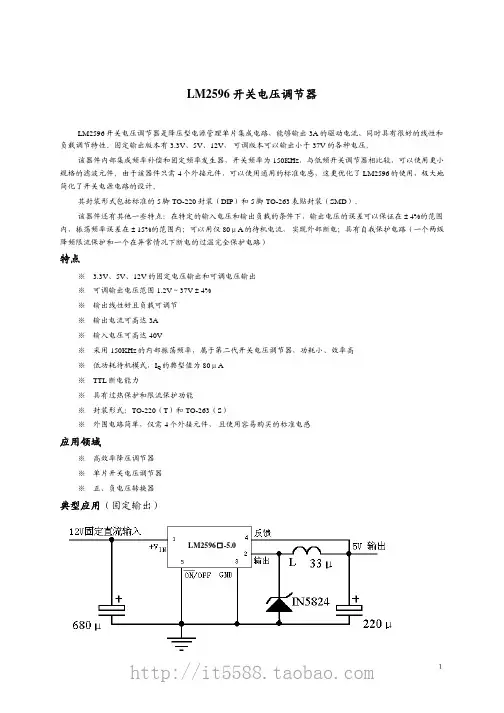

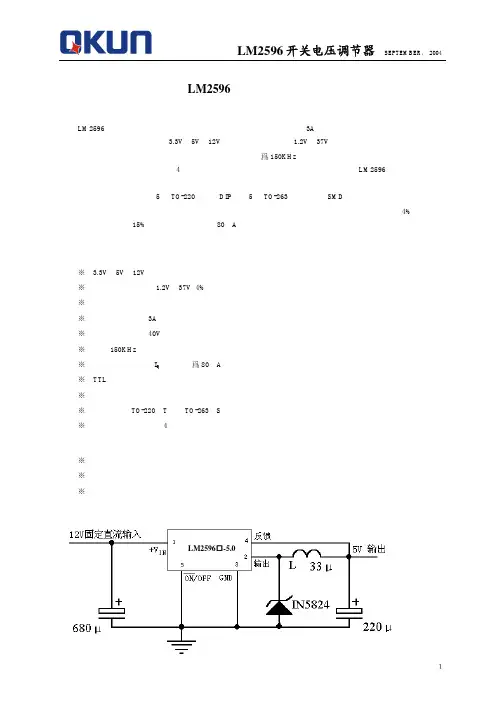
LM2596 开关电压调节器LM2596开关电压调节器是降压型电源管理单片集成电路,能够输出3A的驱动电流,同时具有很好的线性和负载调节特性。
固定输出版本有3.3V、5V、12V,可调版本可以输出小于37V的各种电压。
该器件内部集成频率补偿和固定频率发生器,开关频率为150KHz,与低频开关调节器相比较,可以使用更小规格的滤波元件。
由于该器件只需4个外接元件,可以使用通用的标准电感,这更优化了LM2596的使用,极大地简化了开关电源电路的设计。
其封装形式包括标准的5脚TO-220封装(DIP)和5脚TO-263表贴封装(SMD)。
该器件还有其他一些特点:在特定的输入电压和输出负载的条件下,输出电压的误差可以保证在±4%的范围内,振荡频率误差在±15%的范围内;可以用仅80μA的待机电流,实现外部断电;具有自我保护电路(一个两级降频限流保护和一个在异常情况下断电的过温完全保护电路)特点※ 3.3V、5V、12V的固定电压输出和可调电压输出※可调输出电压范围1.2V~37V±4%※输出线性好且负载可调节※输出电流可高达3A※输入电压可高达40V※采用150KHz的内部振荡频率,属于第二代开关电压调节器,功耗小、效率高※低功耗待机模式,I Q的典型值为80μA※TTL断电能力※具有过热保护和限流保护功能※封装形式:TO-220(T)和TO-263(S)※外围电路简单,仅需4个外接元件,且使用容易购买的标准电感应用领域※高效率降压调节器※单片开关电压调节器※正、负电压转换器典型应用(固定输出)LM2596□-5.0管脚图极限参数名称范围单位最大电源电压 45 V脚输入电压-0.3~25 V“反馈”脚电压 -0.3~25 V到地的输出电压(静态) -1 V功耗由内部限定 --储存温度 -65~150℃静电释放(人体放电1) 2000 V气流焊(60秒) 215 ℃ TO-263红外线焊接(10秒) 245 ℃ 焊接时的管脚温度TO-220 波峰焊/电烙铁焊接(10秒)260℃最高结温 150 ℃温度范围 -40~125℃工 作条 件电源电压 4.5~40 V注1:人体放电模式相当于一个100PF 的电容通过一个1.5K 的电阻向每个管脚放电。
LM2596全中文资料随着电子技术的发展,各种电子设备越来越多,而其中一个重要的电源管理模块就是开关电源。
在电子设备中,开关电源起着将交流电转换为直流电的作用,提供稳定可靠的电力供应。
而LM2596是一种常见的开关稳压模块,它被广泛应用于各种电子设备中,提供高效、稳定的电源管理解决方案。
LM2596是一款具有高效率、低功耗和稳定性的降压型开关稳压模块。
它能够将输入电压转换为相对稳定的输出电压,通常被用于降低电源电压供应至微控制器、电路板、传感器等部件。
同时,LM2596还具备短路保护、过热保护等功能,以确保电子设备的安全运行。
LM2596采用了开关型调制控制技术,能够在不同负载情况下自动调整开关频率和占空比,以保持输出电压稳定。
它的输入电压范围广,可以适应不同的电源输入,包括交流电和直流电。
而输出电压可通过外部电阻分压调整,从而满足不同电子设备的需求。
除了稳压功能,LM2596还具备过流保护功能。
当电流超过设定值时,它会自动切断输出,避免因电流过大而损坏电子设备。
同时,LM2596还配备了过热保护功能,当温度超过一定范围时,它会自动降低工作频率或停止工作,以防止过热引起故障。
LM2596作为一种常见的开关稳压模块,其技术参数和应用案例都有详尽的中文资料可供参考。
对于初学者而言,这些资料不仅提供了LM2596的基本工作原理和使用方法,还介绍了它在各种电子设备中的具体应用场景和性能要求。
其中,电路图、元器件清单和详细的步骤说明,使得初学者能够更好地理解和使用LM2596。
此外,还有一些中文论坛和社区提供了关于LM2596的技术讨论和使用心得的帖子。
这些帖子通常包含了实际应用中遇到的问题和解决方案,对于学习和掌握LM2596的使用具有很大帮助。
在这些中文论坛中,你可以与其他电子爱好者交流经验,共同探讨LM2596的使用技巧。
综上所述,LM2596作为一种常见的开关稳压模块,提供了高效、稳定的电源管理解决方案。
开关型稳压芯片LM2576中文资料LM2576系列开关稳压集成电路是线性三端稳压器件(如78xx系列端稳压集成电路)的替代品,它具有靠得住的工作性能、较高的工作效率和较强的输出电流驱动能力,从而为MCU的稳固、靠得住工作提供了强有力的保证。
LM2576简介LM2576系列是美国国家半导体公司生产的3A电流输出降压开关型集成稳压电路,它内含固定频率振荡器(52kHz)和基准稳压器,并具有完善的爱惜电路,包括电流限制及热关断电路等,利用该器件只需极少的外围器件即可组成高效稳压电路。
LM2576系列包括LM2576(最高输入电压40V)及LM2576HV(最高输入电压60V)二个系列。
各系列产品均提供有、5V、12V(-12)、15V(-15)及可调(-ADJ)等多个电压档次产品。
另外,该芯片还提供了工作状态的外部操纵引脚。
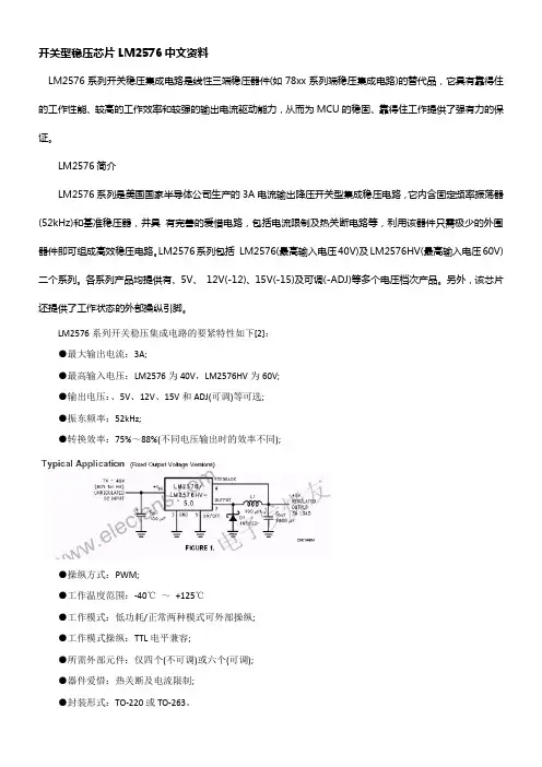
LM2576系列开关稳压集成电路的要紧特性如下[2]:●最大输出电流:3A;●最高输入电压:LM2576为40V,LM2576HV为60V;●输出电压:、5V、12V、15V和ADJ(可调)等可选;●振东频率:52kHz;●转换效率:75%~88%(不同电压输出时的效率不同);●操纵方式:PWM;●工作温度范围:-40℃~+125℃●工作模式:低功耗/正常两种模式可外部操纵;●工作模式操纵:TTL电平兼容;●所需外部元件:仅四个(不可调)或六个(可调);●器件爱惜:热关断及电流限制;●封装形式:TO-220或TO-263。
LM2576的内部框图如图1所示,该框图的引脚概念对应于五脚TO-220封装形式。
LM2576内部包括52kHz振荡器、基准稳压电路、热关断电路、电流限制电路、放大器、比较器及内部稳压电路等。
为了产生不同的输出电压,通常将比较器的负端接基准电压,正端接分压电阻网络,如此可依照输出电压的不同选定不同的阻值,其中R1=1k Ω(可调-ADJ时开路),R2别离为kΩ、kΩ(5V)、kΩ(12V)、kΩ(15V)和0(-ADJ),上述电阻依据型号不同已在芯片内部做了精准调整,因此无需利用者考虑。
LM2596高效开关降压模块
板上带有电源指示发光二极管,蓝色的精密多圈密封式可调电阻,无论工作条件再恶劣也不会影响输出电压的精度。
如果我们把板上的使能跳线帽拔掉,再用单片机的3.3V~5V的电压可以控制模块的第5脚,可以控制LM2596模块的开启或者关闭。
典型工作效率测试如下:12V转5V=(4.93*0.998)/(11.99*0.501)*100%=82.3%(由于测试没考虑线上压降实际输出效率优于测试效率)
性能参数:
核心芯片:LM2596S
体积大小:47*26*14毫米
模块重量:15克
输入电压:4.75~35V
输出电压:1.25~26V任意可调
输出电流:最大3A,可长期工作在2A无需加散热片。
应用领域:数码产品电源系统、太阳能电源处理、LED产品,节能电器等。
LM2596SIMPLE SWITCHER ®Power Converter 150kHz 3A Step-Down Voltage RegulatorGeneral DescriptionThe LM2596series of regulators are monolithic integrated circuits that provide all the active functions for a step-down (buck)switching regulator,capable of driving a 3A load with excellent line and load regulation.These devices are avail-able in fixed output voltages of 3.3V,5V,12V,and an adjust-able output version.Requiring a minimum number of external components,these regulators are simple to use and include internal frequency compensation †,and a fixed-frequency oscillator.The LM2596series operates at a switching frequency of 150kHz thus allowing smaller sized filter components than what would be needed with lower frequency switching regu-lators.Available in a standard 5-lead TO-220package with several different lead bend options,and a 5-lead TO-263surface mount package.A standard series of inductors are available from several dif-ferent manufacturers optimized for use with the LM2596se-ries.This feature greatly simplifies the design of switch-mode power supplies.Other features include a guaranteed ±4%tolerance on out-put voltage under specified input voltage and output load conditions,and ±15%on the oscillator frequency.External shutdown is included,featuring typically 80µA standby cur-rent.Self protection features include a two stage frequency reducing current limit for the output switch and an over tem-perature shutdown for complete protection under fault condi-tions.Featuresn 3.3V,5V,12V,and adjustable output versionsn Adjustable version output voltage range,1.2V to 37V ±4%max over line and load conditions n Available in TO-220and TO-263packages n Guaranteed 3A output load current n Input voltage range up to 40Vn Requires only 4external componentsn Excellent line and load regulation specifications n 150kHz fixed frequency internal oscillator n TTL shutdown capabilityn Low power standby mode,I Q typically 80µA n High efficiencyn Uses readily available standard inductorsn Thermal shutdown and current limit protectionApplicationsn Simple high-efficiency step-down (buck)regulator n On-card switching regulators n Positive to negative converterNote:†Patent Number 5,382,918.Typical Application(Fixed Output Voltage Versions)SIMPLE SWITCHER ®and Switchers Made Simple ®are registered trademarks of National Semiconductor Corporation.DS012583-1December 1997LM2596SIMPLE SWITCHER Power Converter 150kHz 3A Step-Down Voltage Regulator©1999National Semiconductor Corporation 查询LM2596供应商Connection Diagrams and Ordering InformationBent and Staggered Leads,Through HolePackage5-Lead TO-220(T)DS012583-2Order Number LM2596T-3.3,LM2596T-5.0,LM2596T-12or LM2596T-ADJ See NS Package Number T05DSurface Mount Package 5-Lead TO-263(S)DS012583-3Order Number LM2596S-3.3,LM2596S-5.0,LM2596S-12or LM2596S-ADJ See NS Package Number TS5B 2Absolute Maximum Ratings(Note1)If Military/Aerospace specified devices are required, please contact the National Semiconductor Sales Office/ Distributors for availability and specifications. Maximum Supply Voltage45V ON/OFF Pin Input Voltage−0.3≤V≤+25V Feedback Pin Voltage−0.3≤V≤+25V Output Voltage to Ground(Steady State)−1V Power Dissipation Internally limited Storage Temperature Range−65˚C to+150˚C ESD SusceptibilityHuman Body Model(Note2)2kV Lead TemperatureS PackageVapor Phase(60sec.)+215˚C Infrared(10sec.)+245˚C T Package(Soldering,10sec.)+260˚C Maximum Junction Temperature+150˚COperating ConditionsTemperature Range−40˚C≤T J≤+125˚C Supply Voltage 4.5V to40VLM2596-3.3Electrical CharacteristicsSpecifications with standard type face are for T J=25˚C,and those with boldface type apply over full Operating Tempera-ture RangeSymbol Parameter ConditionsLM2596-3.3Units(Limits) Typ(Note3)Limit(Note4)SYSTEM PARAMETERS(Note5)Test Circuit Figure1V OUT Output Voltage 4.75V≤V IN≤40V,0.2A≤I LOAD≤3A 3.3V3.168/3.135V(min)3.432/3.465V(max)ηEfficiency V IN=12V,I LOAD=3A73%LM2596-5.0Electrical CharacteristicsSpecifications with standard type face are for T J=25˚C,and those with boldface type apply over full Operating Tempera-ture RangeSymbol Parameter ConditionsLM2596-5.0Units(Limits) Typ(Note3)Limit(Note4)SYSTEM PARAMETERS(Note5)Test Circuit Figure1V OUT Output Voltage7V≤V IN≤40V,0.2A≤I LOAD≤3A 5.0V4.800/4.750V(min)5.200/5.250V(max)ηEfficiency V IN=12V,I LOAD=3A80%LM2596-12Electrical CharacteristicsSpecifications with standard type face are for T J=25˚C,and those with boldface type apply over full Operating Tempera-ture RangeSymbol Parameter ConditionsLM2596-12Units(Limits) Typ(Note3)Limit(Note4)SYSTEM PARAMETERS(Note5)Test Circuit Figure1V OUT Output Voltage15V≤V IN≤40V,0.2A≤I LOAD≤3A12.0V11.52/11.40V(min)12.48/12.60V(max)ηEfficiency V IN=12V,I LOAD=3A90%3LM2596-ADJElectrical CharacteristicsSpecifications with standard type face are for T J=25˚C,and those with boldface type apply over full Operating Tempera-ture RangeSymbol Parameter ConditionsLM2596-ADJUnits(Limits) Typ(Note3)Limit(Note4)SYSTEM PARAMETERS(Note5)Test Circuit Figure1V FB Feedback Voltage 4.5V≤V IN≤40V,0.2A≤I LOAD≤3A 1.230VV OUT programmed for3V.Circuit of Figure1 1.193/1.180V(min)1.267/1.280V(max)ηEfficiency V IN=12V,V OUT=3V,I LOAD=3A73%All Output Voltage VersionsElectrical CharacteristicsSpecifications with standard type face are for T J=25˚C,and those with boldface type apply over full Operating Tempera-ture Range.Unless otherwise specified,V IN=12V for the3.3V,5V,and Adjustable version and V IN=24V for the12V ver-sion.I LOAD=500mASymbol Parameter ConditionsLM2596-XXUnits(Limits) Typ(Note3)Limit(Note4)DEVICE PARAMETERSI b Feedback Bias Current Adjustable Version Only,V FB=1.3V10nA50/100nA(max) f O Oscillator Frequency(Note6)150kHz127/110kHz(min)173/173kHz(max) V SAT Saturation Voltage I OUT=3A(Notes7,8) 1.16V1.4/1.5V(max) DC Max Duty Cycle(ON)(Note8)100% Min Duty Cycle(OFF)(Note9)0I CL Current Limit Peak Current(Notes7,8) 4.5A3.6/3.4A(min)6.9/7.5A(max)I L Output Leakage Current Output=0V(Notes7,9)50µA(max)Output=−1V(Note10)2mA30mA(max) I Q Quiescent Current(Note9)5mA10mA(max)I STBY Standby QuiescentCurrent ON/OFF pin=5V(OFF)(Note10)80µA200/250µA(max)θJC Thermal Resistance TO-220or TO-263Package,Junction to Case2˚C/W θJA TO-220Package,Junction to Ambient(Note11)50˚C/W θJA TO-263Package,Junction to Ambient(Note12)50˚C/W θJA TO-263Package,Junction to Ambient(Note13)30˚C/W θJA TO-263Package,Junction to Ambient(Note14)20˚C/W ON/OFF CONTROL Test Circuit Figure1ON/OFF Pin Logic Input 1.3VV IH Threshold Voltage Low(Regulator ON)0.6V(max) V IL High(Regulator OFF) 2.0V(min)4All Output Voltage VersionsElectrical Characteristics(Continued)Specifications with standard type face are for T J=25˚C,and those with boldface type apply over full Operating Tempera-ture Range.Unless otherwise specified,V IN=12V for the3.3V,5V,and Adjustable version and V IN=24V for the12V ver-sion.I LOAD=500mASymbol Parameter ConditionsLM2596-XXUnits(Limits) Typ(Note3)Limit(Note4)ON/OFF CONTROL Test Circuit Figure1I H ON/OFF Pin Input Current V LOGIC=2.5V(Regulator OFF)5µA15µA(max) I L V LOGIC=0.5V(Regulator ON)0.02µA5µA(max) Note1:Absolute Maximum Ratings indicate limits beyond which damage to the device may occur.Operating Ratings indicate conditions for which the device is in-tended to be functional,but do not guarantee specific performance limits.For guaranteed specifications and test conditions,see the Electrical Characteristics. Note2:The human body model is a100pF capacitor discharged through a1.5k resistor into each pin.Note3:Typical numbers are at25˚C and represent the most likely norm.Note4:All limits guaranteed at room temperature(standard type face)and at temperature extremes(bold type face).All room temperature limits are100%produc-tion tested.All limits at temperature extremes are guaranteed via correlation using standard Statistical Quality Control(SQC)methods.All limits are used to calculate Average Outgoing Quality Level(AOQL).Note5:External components such as the catch diode,inductor,input and output capacitors,and voltage programming resistors can affect switching regulator sys-tem performance.When the LM2596is used as shown in the Figure1test circuit,system performance will be as shown in system parameters section of Electrical Characteristics.Note6:The switching frequency is reduced when the second stage current limit is activated.The amount of reduction is determined by the severity of current over-load.Note7:No diode,inductor or capacitor connected to output pin.Note8:Feedback pin removed from output and connected to0V to force the output transistor switch ON.Note9:Feedback pin removed from output and connected to12V for the3.3V,5V,and the ADJ.version,and15V for the12V version,to force the output transistor switch OFF.Note10:V IN=40V.Note11:Junction to ambient thermal resistance(no external heat sink)for the TO-220package mounted vertically,with the leads soldered to a printed circuit board with(1oz.)copper area of approximately1in2.Note12:Junction to ambient thermal resistance with the TO-263package tab soldered to a single printed circuit board with0.5in2of(1oz.)copper area.Note13:Junction to ambient thermal resistance with the TO-263package tab soldered to a single sided printed circuit board with2.5in2of(1oz.)copper area. Note14:Junction to ambient thermal resistance with the TO-263package tab soldered to a double sided printed circuit board with3in2of(1oz.)copper area on the LM2596S side of the board,and approximately16in2of copper on the other side of the p-c board.See Application Information in this data sheet and the thermal model in Switchers Made Simple™version4.3software.Typical Performance Characteristics(Circuit of Figure1)NormalizedOutput VoltageDS012583-4Line RegulationDS012583-5EfficiencyDS012583-6 5Typical Performance Characteristics(Circuit of Figure 1)(Continued)Switch Saturation VoltageDS012583-7Switch Current Limit DS012583-8Dropout VoltageDS012583-9OperatingQuiescent CurrentDS012583-10ShutdownQuiescent CurrentDS012583-11Minimum Operating Supply VoltageDS012583-12ON /OFF Threshold VoltageDS012583-13ON /OFF PinCurrent (Sinking)DS012583-14Switching FrequencyDS012583-15 6Typical Performance Characteristics(Circuit of Figure 1)(Continued)Typical Performance CharacteristicsFeedback Pin Bias CurrentDS012583-16Continuous Mode Switching Waveforms V IN =20V,V OUT =5V,I LOAD =2AL =32µH,C OUT =220µF,C OUT ESR =50m ΩDS012583-17A:Output Pin Voltage,10V/div.B:Inductor Current 1A/div.C:Output Ripple Voltage,50mV/div.Horizontal Time Base:2µs/div.Discontinuous Mode Switching Waveforms V IN =20V,V OUT =5V,I LOAD =500mAL =10µH,C OUT =330µF,C OUT ESR =45m ΩDS012583-18A:Output Pin Voltage,10V/div.B:Inductor Current 0.5A/div.C:Output Ripple Voltage,100mV/div.Horizontal Time Base:2µs/div.Load Transient Response for Continuous Mode V IN =20V,V OUT =5V,I LOAD =500mA to 2A L =32µH,C OUT =220µF,C OUT ESR =50m ΩDS012583-19A:Output Voltage,100mV/div.(AC)B:500mA to 2A Load PulseHorizontal Time Base:100µs/div.Load Transient Response for Discontinuous Mode V IN =20V,V OUT =5V,I LOAD =500mA to 2A L =10µH,C OUT =330µF,C OUT ESR =45m ΩDS012583-20A:Output Voltage,100mV/div.(AC)B:500mA to 2A Load PulseHorizontal Time Base:200µs/div.7Test Circuit and Layout GuidelinesAs in any switching regulator,layout is very important.Rap-idly switching currents associated with wiring inductance can generate voltage transients which can cause problems.For minimal inductance and ground loops,the wires indicated by heavy lines should be wide printed circuit traces and should be kept as short as possible.For best results,ex-ternal components should be located as close to the switcher lC as possible using ground plane construction or single point grounding.If open core inductors are used,special care must be taken as to the location and positioning of this type of induc-tor.Allowing the inductor flux to intersect sensitive feedback,lC groundpath and C OUT wiring can cause problems.When using the adjustable version,special care must be taken as to the location of the feedback resistors and the as-sociated wiring.Physically locate both resistors near the IC,and route the wiring away from the inductor,especially an open core type of inductor.(See application section for more information.)Fixed Output Voltage VersionsDS012583-22C IN —470µF,50V,Aluminum Electrolytic Nichicon “PL Series”C OUT —220µF,25V Aluminum Electrolytic,Nichicon “PL Series”D1—5A,40V Schottky Rectifier,1N5825L1—68µH,L38Adjustable Output Voltage VersionsDS012583-23where V REF =1.23VSelect R 1to be approximately 1k Ω,use a 1%resistor for best stability.C IN —470µF,50V,Aluminum Electrolytic Nichicon “PL Series”C OUT —220µF,35V Aluminum Electrolytic,Nichicon “PL Series”D1—5A,40V Schottky Rectifier,1N5825L1—68µH,L38R1—1k Ω,1%C FF —See Application Information SectionFIGURE 1.Standard Test Circuits and Layout Guides 8LM2596Series Buck Regulator Design Procedure(Fixed Output) PROCEDURE(Fixed Output Voltage Version)EXAMPLE(Fixed Output Voltage Version)Given:V OUT=Regulated Output Voltage(3.3V,5V or12V) V IN(max)=Maximum DC Input VoltageI LOAD(max)=Maximum Load Current Given:V OUT=5VV IN(max)=12V I LOAD(max)=3A1.Inductor Selection(L1)A.Select the correct inductor value selection guide from Fig-ures Figure4,Figure5,or Figure6.(Output voltages of3.3V, 5V,or12V respectively.)For all other voltages,see the de-sign procedure for the adjustable version.B.From the inductor value selection guide,identify the induc-tance region intersected by the Maximum Input Voltage line and the Maximum Load Current line.Each region is identified by an inductance value and an inductor code(LXX).C.Select an appropriate inductor from the four manufactur-er’s part numbers listed in Figure8.1.Inductor Selection(L1)e the inductor selection guide for the5V version shown in Figure5.B.From the inductor value selection guide shown in Figure5, the inductance region intersected by the12V horizontal line and the3A vertical line is33µH,and the inductor code is L40.C.The inductance value required is33µH.From the table in Figure8,go to the L40line and choose an inductor part num-ber from any of the four manufacturers shown.(In most in-stance,both through hole and surface mount inductors are available.)2.Output Capacitor Selection(C OUT)A.In the majority of applications,low ESR(Equivalent Series Resistance)electrolytic capacitors between82µF and 820µF and low ESR solid tantalum capacitors between 10µF and470µF provide the best results.This capacitor should be located close to the IC using short capacitor leads and short copper traces.Do not use capacitors larger than 820µF.For additional information,see section on output capaci-tors in application information section.B.To simplify the capacitor selection procedure,refer to the quick design component selection table shown in Figure2. This table contains different input voltages,output voltages, and load currents,and lists various inductors and output ca-pacitors that will provide the best design solutions.C.The capacitor voltage rating for electrolytic capacitors should be at least1.5times greater than the output voltage, and often much higher voltage ratings are needed to satisfy the low ESR requirements for low output ripple voltage.D.For computer aided design software,see Switchers Made Simple™version4.3or later.2.Output Capacitor Selection(C OUT)A.See section on output capacitors in application infor-mation section.B.From the quick design component selection table shownin Figure2,locate the5V output voltage section.In the loadcurrent column,choose the load current line that is closest tothe current needed in your application,for this example,usethe3A line.In the maximum input voltage column,select theline that covers the input voltage needed in your application,in this example,use the15V line.Continuing on this line arerecommended inductors and capacitors that will provide thebest overall performance.The capacitor list contains both through hole electrolytic andsurface mount tantalum capacitors from four different capaci-tor manufacturers.It is recommended that both the manufac-turers and the manufacturer’s series that are listed in thetable be used.In this example aluminum electrolytic capacitors from severaldifferent manufacturers are available with the range of ESRnumbers needed.330µF35V Panasonic HFQ Series330µF35V Nichicon PL SeriesC.For a5V output,a capacitor voltage rating at least7.5V ormore is needed.But even a low ESR,switching grade,220µF10V aluminum electrolytic capacitor would exhibit ap-proximately225mΩof ESR(see the curve in Figure14forthe ESR vs voltage rating).This amount of ESR would resultin relatively high output ripple voltage.To reduce the ripple to1%of the output voltage,or less,a capacitor with a highervalue or with a higher voltage rating(lower ESR)should beselected.A16V or25V capacitor will reduce the ripple volt-age by approximately half. 9LM2596Series Buck Regulator Design Procedure(Fixed Output)(Continued) PROCEDURE(Fixed Output Voltage Version)EXAMPLE(Fixed Output Voltage Version)3.Catch Diode Selection(D1)A.The catch diode current rating must be at least1.3times greater than the maximum load current.Also,if the power supply design must withstand a continuous output short,the diode should have a current rating equal to the maximum current limit of the LM2596.The most stressful condition for this diode is an overload or shorted output condition.B.The reverse voltage rating of the diode should be at least1.25times the maximum input voltage.C.This diode must be fast(short reverse recovery time)and must be located close to the LM2596using short leads and short printed circuit traces.Because of their fast switching speed and low forward voltage drop,Schottky diodes provide the best performance and efficiency,and should be the first choice,especially in low output voltage applications. Ultra-fast recovery,or High-Efficiency rectifiers also provide good results.Ultra-fast recovery diodes typically have re-verse recovery times of50ns or less.Rectifiers such as the 1N5400series are much too slow and should not be used.3.Catch Diode Selection(D1)A.Refer to the table shown in Figure11.In this example,a 5A,20V,1N5823Schottky diode will provide the best perfor-mance,and will not be overstressed even for a shorted out-put.4.Input Capacitor(C IN)A low ESR aluminum or tantalum bypass capacitor is needed between the input pin and ground pin to prevent large volt-age transients from appearing at the input.This capacitor should be located close to the IC using short leads.In addi-tion,the RMS current rating of the input capacitor should be selected to be at least1⁄2the DC load current.The capacitor manufacturers data sheet must be checked to assure that this current rating is not exceeded.The curve shown in Fig-ure13shows typical RMS current ratings for several different aluminum electrolytic capacitor values.For an aluminum electrolytic,the capacitor voltage rating should be approximately1.5times the maximum input volt-age.Caution must be exercised if solid tantalum capacitors are used(see Application Information on input capacitor). The tantalum capacitor voltage rating should be2times the maximum input voltage and it is recommended that they be surge current tested by the manufacturer.Use caution when using ceramic capacitors for input bypass-ing,because it may cause severe ringing at the V IN pin. For additional information,see section on input capaci-tors in Application Information section.4.Input Capacitor(C IN)The important parameters for the Input capacitor are the in-put voltage rating and the RMS current rating.With a nominal input voltage of12V,an aluminum electrolytic capacitor with a voltage rating greater than18V(1.5x V IN)would be needed.The next higher capacitor voltage rating is25V. The RMS current rating requirement for the input capacitor in a buck regulator is approximately1⁄2the DC load current.In this example,with a3A load,a capacitor with a RMS current rating of at least1.5A is needed.The curves shown in Figure 13can be used to select an appropriate input capacitor. From the curves,locate the35V line and note which capaci-tor values have RMS current ratings greater than1.5A.A 680µF/35V capacitor could be used.For a through hole design,a680µF/35V electrolytic capaci-tor(Panasonic HFQ series or Nichicon PL series or equiva-lent)would be adequate.other types or other manufacturers capacitors can be used provided the RMS ripple current rat-ings are adequate.For surface mount designs,solid tantalum capacitors can be used,but caution must be exercised with regard to the ca-pacitor surge current rating(see Application Information on input capacitors in this data sheet).The TPS series available from AVX,and the593D series from Sprague are both surge current tested.10LM2596Series Buck Regulator Design Procedure(Fixed Output)(Continued)Conditions Inductor Output CapacitorThrough Hole Electrolytic Surface Mount Tantalum Output Load Max Input Inductance Inductor Panasonic Nichicon AVX TPS Sprague Voltage Current Voltage(µH)(#)HFQ Series PL Series Series595D Series (V)(A)(V)(µF/V)(µF/V)(µF/V)(µF/V)3.33522L41470/25560/16330/6.3390/6.3722L41560/35560/35330/6.3390/6.31022L41680/35680/35330/6.3390/6.34033L40560/35470/35330/6.3390/6.3622L33470/25470/35330/6.3390/6.3 21033L32330/35330/35330/6.3390/6.34047L39330/35270/50220/10330/10 53822L41470/25560/16220/10330/101022L41560/25560/25220/10330/101533L40330/35330/35220/10330/104047L39330/35270/35220/10330/10922L33470/25560/16220/10330/10 22068L38180/35180/35100/10270/104068L38180/35180/35100/10270/10 1231522L41470/25470/25100/16180/161833L40330/25330/25100/16180/163068L44180/25180/25100/16120/204068L44180/35180/35100/16120/201533L32330/25330/25100/16180/16 22068L38180/25180/25100/16120/2040150L4282/2582/2568/2068/25 FIGURE2.LM2596Fixed Voltage Quick Design Component Selection Table11LM2596Series Buck Regulator Design Procedure(Adjustable Output) PROCEDURE(Adjustable Output Voltage Version)EXAMPLE(Adjustable Output Voltage Version)Given:V OUT=Regulated Output VoltageV IN(max)=Maximum Input VoltageI LOAD(max)=Maximum Load CurrentF=Switching Frequency(Fixed at a nominal150kHz).Given:V OUT=20VV IN(max)=28VI LOAD(max)=3AF=Switching Frequency(Fixed at a nominal150kHz).1.Programming Output Voltage(Selecting R1and R2,asshown in Figure1)Use the following formula to select the appropriate resistorvalues.Select a value for R1between240Ωand1.5kΩ.The lowerresistor values minimize noise pickup in the sensitive feed-back pin.(For the lowest temperature coefficient and the beststability with time,use1%metal film resistors.)1.Programming Output Voltage(Selecting R1and R2,asshown in Figure1)Select R1to be1kΩ,1%.Solve for R2.R2=1k(16.26−1)=15.26k,closest1%value is15.4kΩ.R2=15.4kΩ.2.Inductor Selection(L1)A.Calculate the inductor Volt•microsecond constant E•T(V•µs),from the following formula:where V SAT=internal switch saturation voltage=1.16Vand V D=diode forward voltage drop=0.5Ve the E•T value from the previous formula and matchit with the E•T number on the vertical axis of the InductorValue Selection Guide shown in Figure7.C.on the horizontal axis,select the maximum load current.D.Identify the inductance region intersected by the E•Tvalue and the Maximum Load Current value.Each region isidentified by an inductance value and an inductor code(LXX).E.Select an appropriate inductor from the four manufactur-er’s part numbers listed in Figure8.2.Inductor Selection(L1)A.Calculate the inductor Volt•microsecond constant(E•T),B.E•T=34.2(V•µs)C.I LOAD(max)=3AD.From the inductor value selection guide shown in Figure7,the inductance region intersected by the34(V•µs)horizon-tal line and the3A vertical line is47µH,and the inductorcode is L39.E.From the table in Figure8,locate line L39,and select aninductor part number from the list of manufacturers part num-bers.12LM2596Series Buck Regulator Design Procedure (Adjustable Output)(Continued)PROCEDURE (Adjustable Output Voltage Version)EXAMPLE (Adjustable Output Voltage Version)3.Output Capacitor Selection (C OUT )A.In the majority of applications,low ESR electrolytic or solid tantalum capacitors between 82µF and 820µF provide the best results.This capacitor should be located close to the IC using short capacitor leads and short copper traces.Do not use capacitors larger than 820µF.For additional informa-tion,see section on output capacitors in application in-formation section.B.To simplify the capacitor selection procedure,refer to the quick design table shown in Figure 3.This table contains dif-ferent output voltages,and lists various output capacitors that will provide the best design solutions.C.The capacitor voltage rating should be at least 1.5times greater than the output voltage,and often much higher volt-age ratings are needed to satisfy the low ESR requirements needed for low output ripple voltage.3.Output Capacitor SeIection (C OUT )A.See section on C OUT in Application Information section.B.From the quick design table shown in Figure 3,locate the output voltage column.From that column,locate the output voltage closest to the output voltage in your application.In this example,select the 24V line.Under the output capacitor section,select a capacitor from the list of through hole elec-trolytic or surface mount tantalum types from four different capacitor manufacturers.It is recommended that both the manufacturers and the manufacturers series that are listed in the table be used.In this example,through hole aluminum electrolytic capaci-tors from several different manufacturers are available.220µF/35V Panasonic HFQ Series 150µF/35V Nichicon PL SeriesC.For a 20V output,a capacitor rating of at least 30V or more is needed.In this example,either a 35V or 50V capaci-tor would work.A 35V rating was chosen,although a 50V rat-ing could also be used if a lower output ripple voltage is needed.Other manufacturers or other types of capacitors may also be used,provided the capacitor specifications (especially the 100kHz ESR)closely match the types listed in the table.Re-fer to the capacitor manufacturers data sheet for this informa-tion.4.Feedforward Capacitor (C FF )(See Figure 1)For output voltages greater than approximately 10V,an addi-tional capacitor is required.The compensation capacitor is typically between 100pF and 33nF,and is wired in parallel with the output voltage setting resistor,R 2.It provides addi-tional stability for high output voltages,low input-output volt-ages,and/or very low ESR output capacitors,such as solid tantalum capacitors.This capacitor type can be ceramic,plastic,silver mica,etc.(Because of the unstable characteristics of ceramic capaci-tors made with Z5U material,they are not recommended.)4.Feedforward Capacitor (C FF )The table shown in Figure 3contains feed forward capacitor values for various output voltages.In this example,a 560pF capacitor is needed.13。
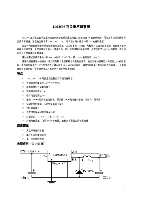
LM2596开关电压调节器LM2596开关电压调节器是降压型电源管理单片集成电路,能够输出3A的驱动电流,同时具有很好的线性和负载调节特性。
固定输出版本有3.3V、5V、12V,可调版本可以输出小于37V的各种电压。
该器件内部集成频率补偿和固定频率发生器,开关频率为150KHz,与低频开关调节器相比较,可以使用更小规格的滤波元件。
由于该器件只需4个外接元件,可以使用通用的标准电感,这更优化了LM2596的使用,极大地简化了开关电源电路的设计。
其封装形式包括标准的5脚TO-220封装(DIP)和5脚TO-263表贴封装(SMD)。
该器件还有其他一些特点:在特定的输入电压和输出负载的条件下,输出电压的误差可以保证在±4%的范围内,振荡频率误差在±15%的范围内;可以用仅80μA的待机电流,实现外部断电;具有自我保护电路(一个两级降频限流保护和一个在异常情况下断电的过温完全保护电路)特点Ć 3.3V、5V、12V的固定电压输出和可调电压输出Ć可调输出电压范围1.2V~37V±4%Ć输出线性好且负载可调节Ć输出电流可高达3AĆ输入电压可高达40VĆ采用150KHz的内部振荡频率,属于第二代开关电压调节器,功耗小、效率高Ć低功耗待机模式,I Q的典型值为80μAĆTTL断电能力Ć具有过热保护和限流保护功能Ć封装形式:TO-220(T)和TO-263(S)Ć外围电路简单,仅需4个外接元件,且使用容易购买的标准电感应用领域Ć高效率降压调节器Ć单片开关电压调节器Ć正、负电压转换器典型应用(固定输出)LM2596□-5.0管脚图极限参数名称范围单位最大电源电压45V 脚输入电压-0.3~25V “反馈”脚电压-0.3~25V 到地的输出电压(静态)-1V 功耗由内部限定--储存温度-65~150℃静电释放(人体放电1)2000V 气流焊(60秒)215℃TO-263红外线焊接(10秒)245℃焊接时的管脚温度TO-220波峰焊/电烙铁焊接(10秒)260℃最高结温150℃温度范围-40~125℃工作条件电源电压4.5~40V注1:人体放电模式相当于一个100PF 的电容通过一个1.5K 的电阻向每个管脚放电。
lm2596中文资料1. 概述lm2596是一款高效率开关电源稳压器芯片,广泛应用于电子设备中对直流电压进行稳定调整的场合。
本文档将详细介绍lm2596的特性、工作原理、应用场景以及使用注意事项。
2. 特性•宽输入电压范围:4V-40V•可调输出电压范围:1.23V-37V•高效率:可达到92%•最大输出电流:3A•过热保护功能3. 工作原理lm2596采用了开关稳压器的工作原理,通过周期性地开关和断开电流流通路径,将输入电压转换为稳定的输出电压。
其主要原理如下:1.输入电压通过电感和开关管传导到输出端,同时电容储存能量。
2.控制器检测输出电压,如果低于设定值,则控制开关管开启,使电流通过电感传输到输出端,提供稳定的输出电压。
3.如果输出电压高于设定值,则控制开关管关闭,切断电流流动。
这种周期性的开关和断开电路,可以通过控制开关管的开启时间和关闭时间,来调整输出电压的稳定性和精确度。
4. 应用场景lm2596广泛应用于各种需要稳定直流电压的场合,以下是lm2596常见的应用场景:4.1 电子设备稳压电源lm2596可以根据需要调整输出电压,可以在电子设备中作为稳压电源芯片使用。
它可以将输入电压调整为稳定的输出电压,以供电子设备正常运行。
4.2 LED照明由于lm2596具有高效率和可调输出电压的特性,非常适合用于LED照明应用。
lm2596可以将输入电压调整为适合LED灯的电压,提供稳定的电源以驱动LED照明。
4.3 高频电源lm2596的高效率和宽输入电压范围,使其非常适合用于高频电源应用。
lm2596可以将输入电压转换为稳定的高频输出,满足高频电源的需求。
5. 使用注意事项在使用lm2596时,请注意以下事项:1.输入电压不要超过40V,否则可能导致芯片过载损坏。
2.充分考虑散热问题,尽量避免芯片过热,建议在芯片周围预留散热空间。
3.在使用lm2596时,应按照芯片的使用说明进行正确的电路设计和连接。