【US20190326508A1】MAGNETICTUNNELJUNCTIONWITHANISOTR
- 格式:pdf
- 大小:2.84 MB
- 文档页数:34

专利名称:Magnetic tunnel junction device withimproved insulating tunnel barrier发明人:Stuart Stephen Papworth Parkin申请号:US09552062申请日:20000419公开号:US06359289B1公开日:20020319专利内容由知识产权出版社提供专利附图:摘要:A magnetic tunnel junction device has a tunnel barrier made of a materialconsisting essentially of an oxide or nitride of one or more of gallium and indium. An oxide or nitride of aluminum may be included as part of this tunnel barrier material. Inone embodiment the tunnel barrier is an oxide of a gallium-aluminum alloy (GaAl). The Ga oxide tunnel barrier may be formed by sputter deposition of Ga, followed by a plasma oxidation, or by depositing Ga from an effusion source in the presence of oxygen gas or in the presence of more reactive oxygen provided by an atomic oxygen source or other source. The tunnel barrier layer may also be formed as a bi-layer structure with an aluminum oxide layer formed directly on one of the ferromagnetic layers of the device, followed by a gallium oxide layer formed directly on the aluminum oxide layer. By appropriate selection of the amounts of gallium and or aluminum, or the thicknesses of the aluminum oxide and gallium oxide in the bi-layer structure, the tunnel barrier energy height can be tuned to a selected value. The magnetic tunnel junction devices made with the improved tunnel barrier material show a substantially reduced tunnel barrier energy height (and thus lower resistance-area values) compared to conventional devices using aluminum oxide tunnel barriers, without a reduction in magnetoresistance.申请人:INTERNATIONAL BUSINESS MACHINES CORPORATION代理人:Thomas R. Berthold更多信息请下载全文后查看。

专利名称:MAGNETIC TUNNEL JUNCTION ANTIFUSE CIRCUIT COMPRISING PARALLELCONNECTED REFERENCE MAGNETICTUNNEL JUNCTIONS TO PROVIDE ANOPTIMUM REFERENCE RESISTANCE发明人:ANDRE, Thomas W.,SUBRAMANIAN, Chitra K.申请号:US2006023123申请日:20060613公开号:WO07/120159P1公开日:20071025专利内容由知识产权出版社提供摘要:An antifuse circuit (10) provides on a per bit basis a signal that indicates whether an MTJ (magnetic tunnel junction) antifuse (18) has been previously programmed to a low resistance state in response to a program voltage. A sense amplifier (12) provides the resistance state signal. A plurality of reference magnetic tunnel junctions (16) are coupled in parallel and to the sense amplifier (12), each (50, 52, 54) having a resistance within a range to provide a collective resistance that can be determined by the sense amplifier (12) to differ from each resistance state of the MTJ antifuse (18). A write circuit selectively provides a current sufficient to create the program voltage when the write circuit (20) is enabled to program the antifuse magnetic tunnel junction (18). Upon detecting a change in resistance in the MTJ antifuse (18), the write circuit (20) reduces current supplied to the antifuse (18). Multiple antifuses may be programmed concurrently. Gate oxide thicknesses of transistors are adjusted for optimal performance.申请人:ANDRE, Thomas W.,SUBRAMANIAN, Chitra K.地址:US,US,US国籍:US,US,US代理机构:KING, Robert L.更多信息请下载全文后查看。

专利名称:MAGNETIC TUNNEL JUNCTION MEMORY CELL ARCHITECTURE发明人:DEBROSSE, John,GOGL,Dietmar,HOENIGSCHMID, Heinz申请号:EP03773669.1申请日:20031028公开号:EP1556863B1公开日:20060322专利内容由知识产权出版社提供摘要:A memory device includes a magnetic tunnel junction memory cell having a magnetic tunnel junction structure (114) and a read switch. In one example, the read switch is connected to a conductor that is used to write to the magnetic tunnel junction structure (104). In a further example, the read switch is a transistor electrically coupled to the magnetic tunnel junction structure by a deep via contact. In a further example, the memory device includes a plurality of magnetic tunnel junction memory cells and a plurality of conductors respectively associated with the cells for writing information to the associated magnetic tunnel junction structures. Each read switch (106) is connected to the conductor (110) associated with a magnetic tunnel junction cell other than the cell in which the read switch resides.申请人:INFINEON TECHNOLOGIES AG,IBM地址:DE,US国籍:DE,US代理机构:Charles, Glyndwr更多信息请下载全文后查看。

专利名称:MAGNETIC TUNNEL JUNCTION SENSORS AND METHODS FOR USING THE SAME 发明人:OSTERFELD, Sebastian J.,WANG, Shan X.申请号:US2014/026506申请日:20140313公开号:WO2014/151820A1公开日:20140925专利内容由知识产权出版社提供专利附图:摘要:Provided are magnetic sensors, which include a magnetic tunnel junction (MTJ) magnetoresistive element, a first electrode contacting at least a portion of a surface of the MTJ magnetoresistive element and extending beyond an edge of the surface of theMTJ magnetoresistive element, and a second electrode contacting at least a portion of an opposing surface of the MTJ magnetoresistive element and extending beyond an edge of the opposing surface of the MTJ magnetoresistive element, where facing surfaces of the extending portions of the first and second electrodes are non-overlapping. Also provided are devices, systems and methods in which the subject magnetic sensors find use.申请人:MAGARRAY, INC.地址:1230 Bordeaux Drive Sunnyvale, California 94089 US国籍:US代理人:NG, Rudy J.更多信息请下载全文后查看。

专利名称:Magnetic Tunnel Junction for MRAMApplications发明人:Wei Cao,Cheng T. Horng,Witold Kula,ChyuJiuh Torng申请号:US14979949申请日:20151228公开号:US20160211442A1公开日:20160721专利内容由知识产权出版社提供专利附图:摘要:A MTJ in an MRAM array is disclosed with a composite free layer having a lower crystalline layer contacting a tunnel barrier and an upper amorphous layer for improvedbit switching performance. According to one embodiment, the amorphous layer has a NiFeM/NiFeMconfiguration where Mand Mare Mg, Hf, Zr, Nb, or Ta, and M1 is unequal to M2. The crystalline layer is Fe, Ni, or FeB with a thickness of at least 6 Angstroms that affords a high magnetoresistive ratio. The Mand Melements in the NiFeMand NiFeMlayers each have a content of 5 to 30 atomic %. The NiFeM/NiFeMconfiguration substantially reduces bit line switching current and number of shorted bits. In an alternative embodiment, the crystalline layer may be a Fe/NiFe bilayer. Annealing at 300°C. to 360° C. provides a high magnetoresistive ratio of about 150%.申请人:Headway Technologies, Inc.地址:Milpitas CA US国籍:US更多信息请下载全文后查看。
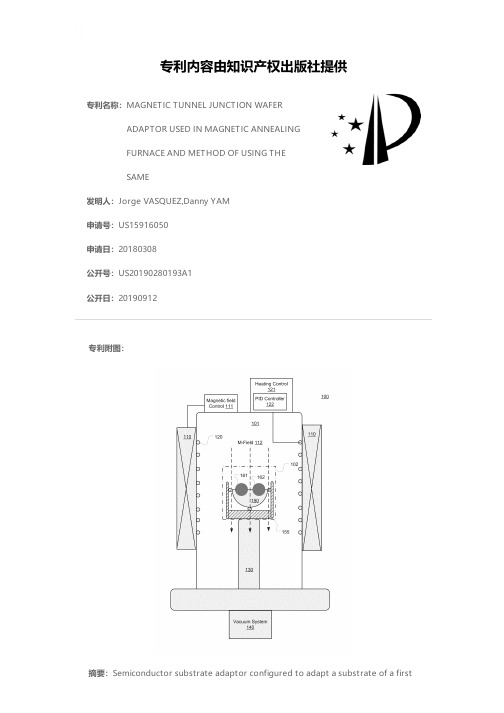
专利名称:MAGNETIC TUNNEL JUNCTION WAFERADAPTOR USED IN MAGNETIC ANNEALINGFURNACE AND METHOD OF USING THESAME发明人:Jorge VASQUEZ,Danny YAM申请号:US15916050申请日:20180308公开号:US20190280193A1公开日:20190912专利内容由知识产权出版社提供专利附图:摘要:Semiconductor substrate adaptor configured to adapt a substrate of a firstdimension to a second dimension, such that the substrate can be properly supported by a supporting mechanism (e.g., a wafer cassette) customized for substrates of the second dimension. The substrate adaptor may be made of quartz. The combination of the substrate adaptor and a substrate fitting therein causes no perturbation in various aspects of a semiconductor process. Therefore, the substrate adaptor conveniently enables a substrate of the first dimension to be processed in the same processing equipment and conditions as a substrate of the second dimension. A vertical substrate adaptor may have a semicircular body with a semicircular cutout for accommodating a wafer and can support a wafer vertically. A horizontal substrate adaptor may have a circular body with a circular cutout for accommodating an entire wafer and supporting the wafer horizontally.申请人:Spin Transfer Technologies, Inc.地址:Fremont CA US国籍:US更多信息请下载全文后查看。
专利名称:Magnetic tunnel junction element andmethod for manufacturing same发明人:Hiroaki Honjo,Tetsuo Endoh,ShojiIkeda,Hideo Sato,Hideo Ohno申请号:US16328852申请日:20170321公开号:US10833256B2公开日:20201110专利内容由知识产权出版社提供专利附图:摘要:A magnetic tunnel junction element includes, in a following stack order, an underlayer formed of a metal material, a fixed layer formed of a ferromagnetic body, amagnetic coupling layer formed of a nonmagnetic body, a reference layer formed of a ferromagnetic body, a barrier layer formed of a nonmagnetic body, and a recording layer formed of a ferromagnetic body, or alternatively, the magnetic tunnel junction element includes, in a following stack order, a recording layer formed of a ferromagnetic body, a barrier layer formed of a nonmagnetic body, a reference layer formed of a ferromagnetic body, a magnetic coupling layer formed of a nonmagnetic body, an underlayer formed of a metal material, and a fixed layer formed of a ferromagnetic body, wherein the fixed layer is formed and stacked after performing plasma treatment to a surface of the underlayer having been formed.申请人:TOHOKU UNIVERSITY地址:Sendai JP国籍:JP代理机构:Westerman, Hattori, Daniels & Adrian, LLP更多信息请下载全文后查看。
专利名称:Magnetic tunnel junction device and methodof manufacturing the same发明人:Shinji Yuasa申请号:US11259371申请日:20051027公开号:US20060176735A1公开日:20060810专利内容由知识产权出版社提供专利附图:摘要:The MR ratio of an MTJ device is increased. A single-crystalline MgO (001)substrate is prepared, and then an epitaxial Fe (001) lower electrode (first electrode) with a thickness of 50 nm is grown on a MgO (001) seed layer at room temperature. Annealingis then performed in ultrahigh vacuum (2×10Pa) at 350° C. A 2-nm thick MgO (001) barrier layer is epitaxially grown on the Fe (001) lower electrode (first electrode) at room temperature, using electron beam evaporation of MgO. A Fe (001) upper electrode (second electrode) with a thickness of 10 nm is then grown on the MgO (001) barrier layer at room temperature, which is successively followed by the deposition of a Co layer with a thickness of 10 nm on the Fe (001) upper electrode (second electrode) The Co layer is used for realizing an antiparallel magnetization alignment by enhancing an exchange bias magnetic field of the upper electrode Thereafter, the above-prepared sample is subjected to microfabrication so as to obtain a Fe (001)/MgO (001)/Fe (001) MTJ device. The density of dislocation defects that exist at the interface between one of the first or the second Fe (001) layer and the single-crystalline MgO (001) layer is not more than 25 to 50 defects/μm.申请人:Shinji Yuasa地址:Ibaraki JP国籍:JP更多信息请下载全文后查看。
专利名称:Magnetic tunnel junction with compensationelement发明人:Yuankai Zheng,Dimitar V. Dimitrov,DexinWang,Wei Tian,Xiaobin Wang,Xiaohua Lou申请号:US12899645申请日:20101007公开号:US08023316B2公开日:20110920专利内容由知识产权出版社提供专利附图:摘要:A magnetic tunnel junction having a compensation element is disclosed. The magnetic tunnel junction includes a synthetic antiferromagnetic reference element, and asynthetic antiferromagnetic compensation element having an opposite magnetization moment to a magnetization moment of the synthetic antiferromagnetic reference element. A free magnetic layer is between the synthetic antiferromagnetic reference element and the synthetic antiferromagnetic compensation element, and an electrically insulating and non-magnetic tunneling barrier layer separates the free magnetic layer from the synthetic antiferromagnetic reference element. The free magnetic layer includes CoFeBwherein X is a value being greater than 30 and Y is a value being greater than 15.申请人:Yuankai Zheng,Dimitar V. Dimitrov,Dexin Wang,Wei Tian,Xiaobin Wang,Xiaohua Lou地址:Bloomington MN US,Edina MN US,Eden Prairie MN US,Bloomington MNUS,Chanhassen MN US,Bloomington MN US国籍:US,US,US,US,US,US代理机构:Campbell Nelson Whipps LLC更多信息请下载全文后查看。