基于FPGA的FSK调制与接收系统设计_谢大川
- 格式:pdf
- 大小:706.68 KB
- 文档页数:2
摘要FPGA是现场可编程门阵列(Field Programmable Gate Array)的简称。
它具有可编程逻辑器件现场可编程的灵活性,又有门陈列器件功能强、高集成度和高速度的优点,因此已在现代通信系统设计中被越来越广泛的应用。
VHDL语言具有很强的电路描述和建模能力,能从多个层次对数字系统进行建模和描述,从而大大简化了硬件设计任务,提高了设计效率和可靠性。
论文着重使用VHDL语言对2FSK的调制与解调进行编程。
在系统仿真中,用MAX+PLUSⅡ作为仿真平台,对2FSK信号进行了调制解调的仿真。
调制方面用的键控法,解调方面用的相干解调进行解调。
基于FPGA的2FSK 调制与解调在MAX+PLUS II上实现,通过VHDL语言的编程,生成调制解调所需要的几个模块,以实现整个2FSK的调制解调系统。
本论文共分四章,第一章主要是介绍了FPGA的原理以及它的应用、发展现状,另外介绍了VHDL语言的特点;第二章较为详细的讲述了FSK 调制和解调的原理,其中包括FSK的多种调制和解调,及功率谱密度的特点。
第三章开始对2FSK调制解调系统的各个单元器件进行设计。
第四章开头介绍了MAX+PLUS II这款软件,接着使用这款软件实现2FSK调制解调算法,其中包括对各个功能模块的算法编程和时序仿真。
本设计的目的不是为了产生一种优于前人算法的算法,而是部分使用前人的算法,在前人算法中加入自己对2FSK调制解调算法的理解,从而产生能用于本设计的非通用算法。
关键词:仿真,2FSK,VHDL,FPGAAbstractFPGA is the abbreviation for Field Programmable Gate Array.It has the flexibility of field programmable to the programmable logic devices,also have strong function, high level of integration and the advantages of high speed,these advantages are same with Gate Array devices.Therefore ,it has been more and more widely used in the modern communication system design.VHDL language has strong ability of circuit described and modeling, it can model and describe digital system in multiple levels,simplified the hardware design task, to improve the design efficiency and reliability.This paper mainly use the language of VHDL on programming modulation and demodulation of 2FSK. In the system simulation,using MAX+PLUSⅡ,to simulate modulation and demodulation of 2FSK. Modulation use keying method, demodulation use coherent demodulation method.Based on 2FSK modulation and demodulation of FPGA realizing on MAX+PLUSⅡ,through the VHDL language programming, producing some blocks of modulation and demodulation,realizing the whole 2FSK modulation and demodulation system.This thesis in chapter 4,The first chapter is mainly introduces he basic principle of FPGA and its application, development situation,also introduces the characteristics of the language of VHDL;the second chapter tells the details of FSK modulation and demodulation basic principle, including various modulation and demodulation method of FSK,and power spectral density characteristics.The third chapter began to design each unit devices of the 2FSK modulation and demodulation.The fourth chapter began to introduce MAX + PLUS II software,using this software to realize the algorithm of 2FSK modulation and demodulation,including programming the algorithm of the function module and timing simulation.The purpose of the design is not to produce an algorithm that better than previous algorithm,but some of the previous algorithm were used,in the previous algorithm to add my 2FSK demodulation of thealgorithm,producing a special algorithms that used on this thesis. Key Words : Simulation; 2FSK; VHDL; FPGA目录摘要 (I)Abstract (II)第一章绪论 (1)1.1 FPGA介绍 (1)1.2 VHDL简介 (2)1.3 论文的目标与内容安排 (3)第二章 FSK调制解调方法 (5)2.1 FSK调制方法 (5)2.1.1 2FSK与MFSK调制 (5)2.2 2FSK调制 (8)2.2.1 模拟调频 (8)2.2.2 键控法 (9)2.3 2FSK解调 (9)2.3.1 相干解调 (9)2.3.2 非相干解调 (10)2.3.3 过零检测 (10)第三章 2FSK调制解调设计 (12)3.1 2FSK调制器设计 (12)3.1.1 功能模块设计 (12)3.1.2 波形的降噪 (14)3.2 2FSK解调器设计 (15)第四章基于max+plusⅡ的2FSK的调制解调算法 (16)4.1 max+plusⅡ软件简介 (16)4.2 2FSK调制解调算法 (16)4.2.1 m序列算法 (16)4.2.2 分频器算法 (18)4.2.3 数据选择器算法 (19)4.2.4 解调器算法 (20)4.2.5 2FSK调制解调完整算法 (22)结束语......................................... 错误!未定义书签。
基于FPGA的FSK调制与接收系统设计【摘要】频移键控是用不同频率的载波来传输数字信号,并用数字基带信号控制载波信号的频率。
二进制频移键控是用两个不同频率的载波来代表数字信号两种电平。
接收端收到不同的载波信号再进行逆变成为数字信号,完成信号的传输过程。
本文主要介绍了一种基于FPGA芯片设计FSK调制解调器的基本原理,并使用相应的VHDL语言对该原理进行描述,该设计以ALTERA公司的大规模集成电路芯片为核心,使得电路简洁、可靠性高。
【关键词】FPGA;FSK;VHDL;大规模集成电路1.选题背景移频键控(FSK)是数字信息传输中使用较早的一种调制形式,它由于其抗干扰及衰落性较好且技术容易实现,因而在集散式工业控制系统中被广泛采用。
以往的键控移频调制解调器采用“固定功能集成电路+连线”方式设计;集成块多,连线复杂,容易出错,且体积较大,本设计采用Lattice公司的FPGA芯片,有效地缩小了系统的体积,降低了成本,增加了可靠性,同时系统采用VHDL-87语言进行设计,具有良好的可移植性及产品升级的系统性。
2.二进制移频键控(2FSK)的基本原理在二进制频移键控中载波频率随着调制信号1或者0而变,1对应于载波频率f1(或者w1),0对应于载波频率f2(或者w2),二进制频移键控已调信号的时域表达式为:其中,=,=是的反码。
2FSK信号波形可以看作两个2ASK信号波形的合成。
图1是相位续的2FSK 信号波形。
3.在FPGA中的FSK实现3.1调制过程的实现首先我们设置了一个输入电平判断器,能够通过不同的输入电平值启动不同的输出端口,调制流程图见图2。
然后根据FSK的特点我们分别设置两个计数器:计数器1和计数器2,其中计数器2的进位频率为计数器1的进位频率的2倍,通过计数器的进位端控制正弦信号发生器的输出频率,这样我们可以通过对两个计数器的切换实现对输出正弦信号频率的控制.首先设计输入电平判断器:输入电平判决器共有一个输入和两个输出端口,根据输入端口电平高低的不同对两个不同的输出口置高电平,其中当某一端口为高电平时另一端口必为低电平,可以设计程序如下:其中din为输入电平端口用于和输入信号相连,dout1和dout2是输出电平端口,用于和下一级电路元件级连作为控制。

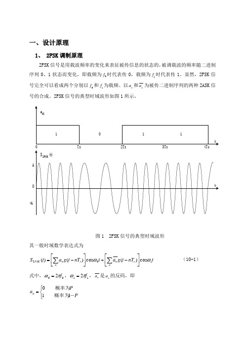
一、设计原理1、 2FSK 调制原理2FSK 信号是用载波频率的变化来表征被传信息的状态的,被调载波的频率随二进制序列0、1状态而变化,即载频为0f 时代表传0,载频为1f 时代表传1。
显然,2FSK 信号完全可以看成两个分别以0f 和1f 为载频、以n a 和n a 为被传二进制序列的两种2ASK 信号的合成。
2FSK 信号的典型时域波形如图1所示,-A图1 2FSK 信号的典型时域波形其一般时域数学表达式为t nT t g a t nT t g a t S n s n n s n FSK 102cos )(cos )()(ωω⎥⎦⎤⎢⎣⎡-+⎥⎦⎤⎢⎣⎡-=∑∑ (10-1)式中,002f πω=,112f πω=,n a 是n a 的反码,即⎩⎨⎧=PP a n -概率为概率为11⎩⎨⎧=PP a n -概率为概率为1012、用FPGA 实现2FSK 调制器的方案采用键控法实现2FSK ,功能模块设计如图2所示。
图2 用FPGA 实现2FSK 调制器方案通过不同的分频器,产生频率分别为f1和f2的基频。
基带信号为“1”时,频率f1的信号通过;当基带信号为“0”时,频率f2的信号通过。
f1和f2作为正弦表的地址发生器的时钟,正弦表输出正弦波的样点数据,经过D/A 数模转换,得到连续的2FSK 信号。
3、 程序设计原理本实验制作一个基于FPGA 的2FSK 调制器,其设计原理图如图2所示。
程序整体由四个子模块构成:正弦波形模块,采用64个点作为一个波形的数据周期,即正弦波的一个周期的波形采样为64个点;100KHz 分频模块,利用FPGA 上50MHz 的晶振分频得到,作为正弦波形的频率f1;400KHz 分频模块,利用FPGA 上50MHz 的晶振分频得到,作为正弦波形信号的频率f2;1Hz 分频模块,利用PGA 上27MHz 的晶振分频得到,作为频率f1或f2的选择信号。
电路图如图3所示:图3 电路原理图二、源程序代码//顶层模块module FSK(clk_50M,clk_27M,reset,sin_out);input clk_50M,clk_27M,reset;output[7:0] sin_out;wire clk_100K,clk_400K,clk,flag;divider1 U1(clk_100K,reset,clk_50M);divider2 U2(clk_400K,reset,clk_50M);select_clk U3(clk,flag,reset,clk_27M,clk_100K,clk_400K); sin U4(clk,reset,sin_out);endmodule//分频器1 f1(100KHz)module divider1(clk_100K,reset,clk_50M);output clk_100K;input reset,clk_50M;reg clk_100K;reg[23:0] cnt;always @(posedge clk_50M)beginif (reset)begincnt<=0; //同步复位clk_100K<=0;endelse if(cnt==249)begincnt<=0;clk_100K<=~clk_100K;endelsecnt<=cnt+1; //计数endendmodule//分屏器2 f2(400kHz)module divider2(clk_400K,reset,clk_50M);output clk_400K;input reset,clk_50M;reg clk_400K;reg[23:0] cnt;always @(posedge clk_50M)beginif (reset)begincnt<=0; //同步复位clk_400K<=0;endelse if(cnt==42)begincnt<=0;clk_400K<=~clk_400K;endelsecnt<=cnt+1; //计数endendmodule//分屏器3 (1Hz,用来选频)module select_clk(clk,flag,reset,clk_27M,clk_100K,clk_400K); input clk_100K,clk_400K,clk_27M,reset;output clk,flag;reg clk,flag;reg[23:0] cnt;always @(posedge clk_27M)beginif (reset)begincnt<=0; //同步复位flag<=0;endelse if(cnt==13499999)begincnt<=0;flag<=~flag;endelsecnt<=cnt+1; //计数case(flag)0:clk<=clk_100K; //用来选择正弦信号的频率1:clk<=clk_400K;endcaseendendmodule//正弦波形模块module sin(clk,reset,sin_out);input clk,reset;output[7:0] sin_out;reg[7:0] sin_out;reg[6:0] num;always@(posedge clk or posedge reset)beginif(reset)sin_out<=0;else if(num==63)num<=0;elsenum<=num+1;case(num)0:sin_out<=255;1:sin_out<=254;2:sin_out<=252;4:sin_out<=245; 5:sin_out<=239; 6:sin_out<=233; 7:sin_out<=225; 8:sin_out<=217; 9:sin_out<=207; 10:sin_out<=197; 11:sin_out<=186; 12:sin_out<=174; 13:sin_out<=162; 14:sin_out<=150; 15:sin_out<=137; 16:sin_out<=124; 17:sin_out<=112; 18:sin_out<=99; 19:sin_out<=87; 20:sin_out<=75; 21:sin_out<=64; 22:sin_out<=53; 24:sin_out<=43; 24:sin_out<=34; 25:sin_out<=26; 26:sin_out<=19; 27:sin_out<=13; 28:sin_out<=8; 29:sin_out<=4; 30:sin_out<=1; 31:sin_out<=0; 32:sin_out<=0; 33:sin_out<=1; 34:sin_out<=4; 35:sin_out<=8; 36:sin_out<=13; 37:sin_out<=19; 38:sin_out<=26; 39:sin_out<=34; 40:sin_out<=43; 41:sin_out<=53; 42:sin_out<=64; 43:sin_out<=75; 44:sin_out<=87; 45:sin_out<=99; 46:sin_out<=112;48:sin_out<=137;49:sin_out<=150;50:sin_out<=162;51:sin_out<=174;52:sin_out<=186;53:sin_out<=197;54:sin_out<=207;55:sin_out<=217;56:sin_out<=225;57:sin_out<=233;58:sin_out<=239;59:sin_out<=245;60:sin_out<=249;61:sin_out<=252;62:sin_out<=254;63:sin_out<=255;default:sin_out<=8'bx;endcaseendendmodule三、仿真结果1、分屏器模块仿真结果如图4所示:图4 分屏器模块仿真结果2、正弦波形模块仿真结果如图5所示:图5 正弦波形模块仿真结果图6 最终波形输出结果图7 modelsim仿真波形图四、实验结果利用DE2上的拓展引脚,接到单片机上的数/模转换芯片DAC0832,再用示波器测试芯片的输出引脚查看波形,结果如图8和图9所示:图8 频率为f1的正弦波形图9 频率为f2的正弦波形图10 混合波形图从以上分析可知,该设计实现了2FSK调制器的功能:基带信号为“1”时,频率f1的信号通过;当基带信号为“0”时,频率f2的信号通过。
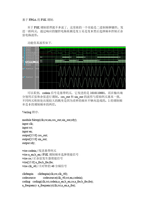
基于FPGA的FSK调制:至于FSK调制原理就不多说了,这里做的一个实验是二进制频移键控。
发送一组码元,通过响应的键控电路监测是发1还是发0然后选择频率控制正余弦电路波形。
功能仿真波形如下:可以看到,codein信号是基带码元,它发送的是1010110001,而在输出端分别用正弦和余弦进行调制。
cos_out和sin_out的波形与原始码元基本一致,不同码元衔接处出现较大的跳变是因为采样的频率不够高造成的。
1的调制频率是0的调制频率的两倍。
Verilog程序:module fsktop(clk,rst,en,cos_out,sin_out,rdy);input clk;input rst;input en;output[15:0] cos_out;output[15:0] sin_out;output rdy;wire codein;//发送基带码元wire a_en,b_en;//FSK调制频率选择使能信号wire ce;//正余弦发生器使能信号wire[15:0] a_fre,b_fre,fre;wire clk_40;//主时钟的40分频信号clkfenpin clkfenpin(clk,rst,clk_40);codesource codesource(clk_40,rst,en,codein);coding coding(clk,rst,codein,a_en,b_en,ce,a_fre,b_fre,fre);a_frequency a_frequency(clk,rst,a_en,a_fre);b_frequency b_frequency(clk,rst,b_en,b_fre);cos cos(fre,clk,ce,cos_out,sin_out,rdy);endmodulemodule clkfenpin(clk,rst,clk_40);input clk;input rst;output clk_40;reg[4:0] num;reg clk_40;always @ (posedge clk)beginif(rst) begin num <= 5'd0; clk_40 <= 0; endelsebeginnum <= num+1;if(num==5'd19) begin num <= 5'd0; clk_40 <=~clk_40; end endendendmodulemodule codesource(clk_40,rst,en,codein);input clk_40;input rst;input en;output codein;//发送基带码元reg codein;reg[15:0] source;//从高到低连续发送该16bit码元信号reg[3:0] num;always @ (posedge clk_40)beginif(rst)beginsource <= 16'b1010110001110010;codein <= 1'bx;num <= 4'b1111;endelse if(en)begincodein <= source[num];num <= num-1;endelsebeginsource <= 16'b1010110001110010;codein <= 1'bx;num <= 4'b1111;endendendmodulemodule coding(clk,rst,codein,a_en,b_en,ce,a_fre,b_fre,fre);input clk;input rst;input codein;input[15:0]a_fre,b_fre;output[15:0] fre;output a_en,b_en;output ce;reg a_en,b_en;reg ce;reg[15:0] fre;always @ (posedge clk)beginif(rst)begina_en <= 0;b_en <= 0;ce <= 0;fre <= 16'd0;endelse if(!codein) //基带码元为0时,选择a_fre为输出频率beginfre <= a_fre;a_en <= 1;b_en <= 0;ce <= 1;endelse if(codein) //基带码元为1时,选择b_fre为输出频率beginb_en <= 1;a_en <= 0;ce <= 1;fre <= b_fre;endelsebegina_en <= 0;b_en <= 0;ce <= 0;fre <= 16'd0;endendendmodulemodule a_frequency(clk,rst,a_en,fre);input clk;input rst;input a_en;output[15:0] fre;reg[15:0] fre;always @ (posedge clk)beginif(rst) begin fre <= 16'h9b82; end//-pielse if(a_en)beginif((fre<16'h8000)&&(fre>16'h6087)) fre <= 16'h9b82;else fre <= fre+16'h0506;endelse begin fre <= 16'h9b82; endendendmodulemodule b_frequency(clk,rst,b_en,fre);input clk;input rst;input b_en;output[15:0] fre;reg[15:0] fre;always @ (posedge clk)beginif(rst) begin fre <= 16'h9b82; end//pielse if(b_en)beginif((fre<16'h8000)&&(fre>16'h6087)) fre <= 16'h9b82;else fre <= fre+16'h0a0c;endelse begin fre <= 16'h9b82; endendendmodule调用了IP Core中的cos_sin生成函数。
基于FPGA的FSK调制解调系统设计摘要数字调制技术作为通信技术领域中极为重要的一个方面,得到了迅速发展。
随着数字调制技术的出现,在有限的带宽内传输高速的数据已成为可能。
在数字传输系统中,数字信号对高频载波进行调制,变为频带信号,通过信道传输,在接收端解调后恢复成数字信号。
FSK是数据通信中使用较早的一种通信方式。
由于这种调制解调方式容易实现,抗噪声和抗衰减性能较强,因此在中低速数据传输通信系统中得到较为广泛的应用。
本文首先介绍了2FSK调制与解调的工作原理,以及VHDL程序设计和仿真方法。
在此基础上,本文给出了2FSK调制与解调的具体实现方法以及实验结果,并进行了分析和讨论。
然后详细介绍了基于FPGA的2FSK信号发生器的设计方法,提供了VHDL 源代码在QuartusⅡ环境下的仿真结果。
整个系统的功能在EDA技术开发平台上调试通过,具有较高的实用性和可靠性。
关键词:FPGA,CPLD,调制,解调,2FSKTHE DESIGN OF FSK MODEM BASED ON FPGAABSTRACTDigital modulation techniques in the field of communication technology as a very important aspect has been developing rapidly. With the emergence of digital modulation techniques, in the limited bandwidth and high-speed data transmission possible. In digital transmission systems, digital signal modulation of high-frequency carrier, into a band signal transmission through the channel in the receiver demodulation into a digital signal after the resumption. FSK is used in data communications as a means of communication earlier. As a result of this approach easy to implement modem, anti-noise and anti-decay properties of strong, so low-speed data transmission in the communication system to be more widely used.This article introduced the first modulation and demodulation 2FSK working principle, as well as the VHDL design and simulation methods. On this basis then, this paper 2FSK specific modulation and demodulation method and experimental results and an analysis and discussion. Details of FPGA-based signal generator 2FSK the design methodology, VHDL source code provided in the Quartus Ⅱsimulation environment. The entire system technology development in EDA platform debugging through high practicality and reliability.KEYWORDS: FPGA,CPLD,modulation,demodulation,2FSK目录摘要 (I)1 绪论 (1)1.1研究背景 (1)1.2研究思路和方案分析 (1)1.3主要研究内容 (3)2 可编程片上系统开发技术 (5)2.1可编程逻辑器件及硬件描述语言VHDL (5)2.1.1可编程逻辑器件简介 (5)2.1.2硬件描述语言VHDL简介 (6)2.2可编程片上系统技术 (8)2.3Q UARTUS Ⅱ介绍 (10)3 FSK调制解调原理 (12)3.1二进制频移键控信号的调制原理 (12)3.2二进制频移键控信号的解调原理 (14)3.3载波信号发生器原理 (15)4 调制解调器系统的实现 (18)4.1系统整体分析 (18)4.2调制部分 (19)4.2.1 四位可预置二进制减计数器 (19)4.2.2 正弦波合成器 (20)4.2.3 调制仿真 (21)4.3解调部分 (22)4.3.1 同步脉冲发生器 (22)4.3.2 计数器 (23)4.3.3 判别锁存电路 (24)4.3.4 解调仿真 (25)4.4本章小结 (26)5 总结与展望 (27)参考文献 (28)致谢 (29)1 绪论1.1 研究背景通信技术融入计算机和数字信号处理技术以后发生了革命性的变化,它和计算机技术、信号处理技术结合是现代通信技术的标志。
基于FPGA的FSK调制解调系统设计郑争兵【期刊名称】《陕西理工学院学报(自然科学版)》【年(卷),期】2012(028)005【摘要】根据FSK调制和解调的工作原理,提出了一种基于FPGA芯片的FSK调制解调器.该系统采用键控法设计调制器模块,利用过零检测法实现解调器模块.利用VHDL语言在Altera公司的Cyclone系列的EP1C12Q240C6芯片上软件编程,完成了整个系统相应的时序仿真.硬件实验测试表明:FSK解调信号波形和调制信号波形一致,二者之间存在一定的延时,满足系统的设计要求,整个系统具有较高的可靠性和移植性.%An FSK modem based on FPAG chip is proposed by the principle of FSK modulation and demodulation. The modulator module is designed by the keying method and the demodulator module is realized by the zero-crossing detection method in the system. The software programming is done by VHDL language in the Altera's Cyclone series chip EP1C12Q240C6, then the appropriate timing simulation of the entire system is finished. The hardware testing shows that there is a certain delay but no difference between FSK demodulation signal waveform and modulation signal waveform to meet system design requirements, so the entire system has high reliability and portability.【总页数】5页(P20-24)【作者】郑争兵【作者单位】陕西理工学院物理与电信工程学院,陕西汉中723003【正文语种】中文【中图分类】TN92【相关文献】1.基于FPGA的FSK调制解调系统设计 [J], 杨湲;肖顺文;邹贵祥;易欢;李怡琳2.基于FPGA的FSK调制解调器设计 [J], 孙志雄;谢海霞3.基于FPGA的FSK调制解调系统设计与实现 [J], 耿家国4.基于FPGA的2FSK调制解调器设计与仿真 [J], 李桂枝;黄鸿捷;谢文娣5.基于FPGA的FSK调制解调系统设计 [J], 杨湲;肖顺文;邹贵祥;易欢;李怡琳因版权原因,仅展示原文概要,查看原文内容请购买。
第 21 卷 第 7 期2023 年 7 月太赫兹科学与电子信息学报Journal of Terahertz Science and Electronic Information TechnologyVol.21,No.7Jul.,2023基于FPGA的2CPFSK全数字中频调制器的设计与实现廖治宇,王鹏(中国工程物理研究院电子工程研究所,四川绵阳621999)摘要:针对飞行器数据链中高码速率要求,需要使用数字技术实现传统模拟调制,以得到更好的调制性能,增加系统作用距离。
本文介绍了二进制连续相位频移键控(2CPFSK)调制原理,提出了基于软件无线电架构的2CPFSK正交调制算法。
该算法利用2CPFSK相位累加特性实现了基带数据的分数倍内插,从而适应宽范围码速率的调制。
设计了提高频谱纯度的数字滤波器、基于FPGA+DAC架构的数字调制器硬件平台并实现算法。
通过与传统模拟频率调制(FM)比较,该设计提升了1.7 dB调制性能,增加了系统作用距离。
关键词:二进制连续相位调制;数字中频调制;分数倍内插;高斯成型滤波中图分类号:TN791.1 文献标志码:A doi:10.11805/TKYDA2020701 Design and implementation ofDesign and implementation of 22CPFSK full digital intermediate frequencymodulator based on FPGALIAO Zhiyu,WANG Peng(Institute of Electronic Engineering,China Academy of Engineering Physics,Mianyang Sichuan 621999,China)AbstractAbstract::The digital modulation is necessary in order to meet the requirement of higher signal transmission rate in aerocraft data link. The better modulating performance and the longercommunication distance can be achieved by digital modulation. The principle of 2 Continuous PhaseFrequency Shift Keying(CPFSK) modulation with binary continuous phase is introduced. A 2CPFSKquadrature modulation algorithm based on software radio architecture is proposed.By using the phaseaccumulation property of 2CPFSK, the algorithm realizes the fractional interpolation of baseband data toadapt to the modulation of wide range code rate.A digital filter is also designed to improve spectralpurity. The hardware platform of digital modulator based on Field Programmable Gate Array+Digital-to-Analog Converter(FPGA+DAC) architecture is designed and the algorithm is paredwith traditional analog Frequency Modulation(FM), this design improves the link performance by 1.7 dBand increases the communication distance of the system.KeywordsKeywords::2 Continuous Phase Frequency Shift Keying;digital intermediate frequency modulation;fractional interpolation;Gaussian shaping filter二进制连续相位频移键控(2CPFSK)技术以其良好的抗噪声和抗衰落性能,以及实现容易、解调设备比移相键控(Phase Shift Keying,PSK)简单(可直接使用频率调制(FM)解调设备),信号所占的频带比2PSK小等特点,在无线通信领域中占有相当的优势,但在国内飞行器数据链中却未得到很好的应用[1]。
基于FPGA的FSK调制解调系统设计与实现作者:耿家国来源:《科技风》2018年第06期摘要:FPGA技术在电子通信领域得到了越来越广泛的应用,并已逐渐成为电子产品实现的首选方案。
FSK(Frequency Shift Keying二进制移频键控)是数字通信中使用较早的一种调制方式,它用不同频率的载波来传递信号,用数字基带信号来控制载波信号的频率。
论文详细介绍了基于FPGA的FSK调制解调系统的设计和实现,整个设计基于ALTERA公司的QuartusⅡ开发平台,并用Cyclone系列FPGA实现。
经测试,系统能正常工作。
关键词:FPGA ;FSK;调制解调;Quartus IIFPGA不仅具有可编程门阵列的高可靠性,而且具有用户可编程性的特点,这种可编程特性带来了数字电路设计的灵巧性,在数字电路设计中起着非常重要的作用。
FSK是通信传输中使用较早的一种调制方法。
它有抵抗噪声能力好、传输的距离比较远、传输的误码率低等特点。
传统的使用硬件手段实现FSK,特别是在相干解调模块需要对其提取数字载波时,需要的设备比较复杂,而且成本较高,本文通过QuartusII 软件平台,采用VHDL语言,设计并实现了一种FSK调制解调系统。
1 系统整体设计系统整体分为两大部分:FSK调制和FSK解调。
如下图所示。
FSK调制包括分频器模块、M序列发生器模块、选通开关模块。
FSK解调包括微分模块、脉冲展宽模块、低通滤波模块、位同步模块。
2 系统功能实现(1)调制电路由分频器模块、M序列模块、二选一选择器模块组成,选用M序列的阶数为5,采用D触发器和门电路组成,异或门为线性反馈电路,门电路和非门来保证全零时系统可以自动启动。
(2)微分模块使用两个D触发器、一个非门和一个与门来实现对输入宽脉冲信号的微分功能。
(3)脉冲展宽模块采用VHDL语言和电路原理图混合输入设计,其中计数器利用VHDL 硬件描述语言来实现。
(4)数字滤波器采用设计优化好的FIR滤波器的IP核。